N A N O E X P R E S S
Open Access
Great blue-shift of luminescence of ZnO
nanoparticle array constructed from ZnO
quantum dots
Nengwen Wang, Yuhua Yang and Guowei Yang
*Abstract
ZnO nanoparticle array has been fabricated on the Si substrate by a simple thermal chemical vapor transport and condensation without any metal catalysts. This ZnO nanoparticles array is constructed from ZnO quantum dots (QDs), and half-embedded in the amorphous silicon oxide layer on the surface of the Si substrate. The
cathodoluminescence measurements showed that there is a pronounced blue-shift of luminescence comparable to those of the bulk counterpart, which is suggested to originate from ZnO QDs with small size where the quantum confinement effect can work well. The fabrication mechanism of the ZnO nanoparticle array constructed from ZnO QDs was proposed, in which the immiscible-like interaction between ZnO nuclei and Si surface play a key role in the ZnO QDs cluster formation. These investigations showed the fabricated nanostructure has potential
applications in ultraviolet emitters.
Introduction
Recently, ZnO has attracted very great attention because of its particular properties in broad fields. For example, it has a large direct band gap of 3.37 eV and exciton-binding energy of 60 meV, while the Bohr radius of exciton is as small as approx. 2.34 nm. Thus, ZnO is a promising candidate for the high efficient ultraviolet (UV) laser device [1-3]. Interestingly, when the size of ZnO nanoparticles is smaller than the Bohr radius (i.e., ZnO quantum dots, QDS), the quantum confinement has a notable influence on the band gap and further causes a series of novel characteristics such as the blue-shift of luminescence [4-7]. Therefore, there have been a variety of techniques to fabricate ZnO QDs [6-10]. Usually, the size of ZnO QDs is slightly larger than or just comparable with the exciton Bohr radius [8-13]. However, few research reports have been involved in the ZnO QDs, showing that their dimension is rigorously smaller than the Bohr radius [4-13].
In this study, we have fabricated the unique ZnO nanoparticle arrays that are constructed from ZnO QDs
blocks on silicon substrates using a simple thermal che-mical vapor transport and condensation without any metal catalysts. Importantly, we measure a great blue-shift of luminescence in the cathodoluminescence (CL) spectrum of the fabricated nanostructure, which implies that this ZnO QDs structure would be applicable to optoelectronic and spintronic applications.
Experimental
The ZnO nanoparticle array is fabricated by a simple thermal vapor transport method, and the detailed experimental process has been reported in our previous study [13]. Simply, Si wafers serving as substrates are loaded downstream in a quartz tube. Zinc oxide pow-ders and graphite powpow-ders are mixed and heated to 1050°C under the argon gas flow at the rate of 50 sccm with a pressure of 9.0 × 10⁴ Pa. Half-an-hour later, the source powders and the substrate are all taken out from the furnace and allowed to cool down to room tempera-ture naturally. Field emission scanning electron
micro-scopy (FESEM), X-ray diffraction (XRD), and
transmission electron microscopy (TEM) coupled with electron-energy loss spectroscopy (EELS) are employed to characterize the morphologies and structures of the prepared samples. The CL measurement is carried out at room temperature using a Gatan Mono-CL system * Correspondence: [email protected]
State Key Laboratory of Optoelectronic Materials and Technologies, Institute of Optoelectronic and Functional Composite Materials, Nanotechnology Research Center, School of Physics & Engineering, Sun Yat-sen University, Guangzhou 510275, Guangdong, P. R. China
Wanget al.Nanoscale Research Letters2011,6:338 http://www.nanoscalereslett.com/content/6/1/338
coupled to FESEM with the accelerating voltage of 10 kV.
Results and discussion
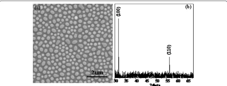
The fabricated nanoparticle array is shown in Figure 1. Clearly, these nanoparticles are relatively uniform in size and array, isolated, and elliptical. They are half-embedded in the surface of the Si substrate. The corre-sponding XRD pattern (Figure 1b) can be indexed to be the wurtzite ZnO structure with (100) and (110) peaks. Therefore, these results show that the prepared nano-particles are ZnO. Note that we can control the size of the fabricated nanoparticles by the growth conditions such as the growth time.
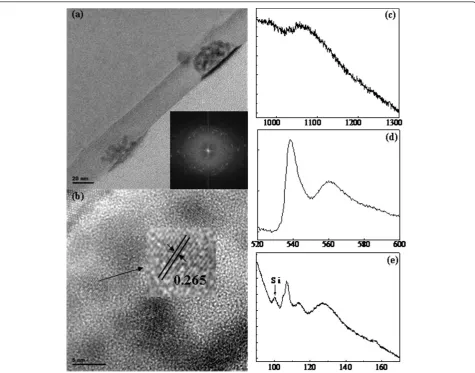
In order to verify the detailed structure of the fabri-cated nanoparticle array, we prepare the cross-sectional sample for TEM characterization, and the results are shown in Figure 2. In the low magnification of TEM image in Figure 2a, the thickness of the layer is uniform of approx. 25 nm, while two high contrast particles are implanted in the layer. The sizes of the two particles are, respectively, 50 and 57 nm at the interface. The FFT pattern (the inset of Figure 2a) of one particle indi-cates that it is polycrystalline. The HRTEM image in Figure 2b is taken from the upper ZnO nanoparticle in Figure 2a. Clearly, we can see that several small crystal-line particles gather together and form one nanoparticle. The average size of these small ZnO particles is 5.5 nm, which are the so-called ZnO QDs [4-13]. One ZnO QD has been emphasized and marked with the interplanar spacing of 0.265 nm in the inset of Figure 2b, which is corresponding to the plane (002) of the wurtzite ZnO. Actually, all the interplanar spacings of QDs in Figure 2b and other HRTEM data can be assigned to the
spacings of the wurtzite ZnO structure. In addition, we can easily observe that these ZnO QDs are embedded in the amorphous silicon oxide layer on the surface of the Si substrate. Therefore, these results show that the fabri-cated ZnO nanoparticle array is constructed from ZnO QDs.
The EELS spectra of the Zn-L, O-K, and Si-L edges on the particle zone of the sample exhibited in Figure 2c,d,e show that the ZnO nanoparticles contain Zn, O, and Si elements. The sets of Zn-L edge with the peak centered at 1050 eV and the O-K edge with the feature peak at 538 eV demonstrate that the nanoparticles are zinc oxide, in accordance with reports and the analytic results shown above, while the spectra shift due to the native defects, such as Zn and O vacancies on the sur-face of ZnO QDs [14-17]. As we see the Si-L edge in Figure 2e, the distinct features are at 100, 107, 114, 127, and 157 eV, respectively. This Si-L edge is very similar with the spectrum of silicon monoxide that is
over-lapped by spectra of elemental silicon and of SiO2
whose onsets of the L2,3-edge are approx. 100 and 107
eV, respectively [18-23]. Thus, these results reveal that the ZnO QDs disperse in the silicon monoxide.
In order to explore this fabricated nanostructure’s
[image:2.595.58.538.88.271.2]potential applications, we measure the optical properties as shown in Figure 3. Figure 3 shows the CL measure-ment of the sample. The panchromatic CL image in Figure 3b exhibits that the intense luminescence is mainly from the ZnO nanoparticles. Interestingly, we can observe that the luminescence peak is centered at 363 nm as shown in Figure 3c, which is known as the near-band edge emission of ZnO. However, there is a great blue-shift compared to bulk ZnO in the CL spectrum. Based on previous reports [1,10,24,25], the
blue-shift of the CL spectrum of ZnO QDs in our stu-dies is attributed to the quantum-size confinement effect as follows [5,26]
E(gap,dot)=E(gap,bulk)+π 2h¯2
2R2
1
m∗e
+ 1
m∗h
−0.248E∗Ryd (1)
where ћis the Planck’s constant, R is the radius of ZnO QDs, m∗eand m∗h are, respectively, the effective
masses of electron and hole (takingm∗e= 0.24m0and
m∗h= 1.8m0[27]), E(gap, bulk) is the bulk ZnO band gap
(3.377 eV), and E∗Rydis the exciton-binding energy (60 meV [2]). Based on Equation 1, we can obtain the rela-tionship between the size and band gap of ZnO QDs as shown in Figure 4. In our case, the radius of ZnO QDs is in the range of 1.6-6.1 nm are also shown in Figure 4. The corresponding band gap and emission wavelength ranges of the prepared ZnO QDs with the radius of
[image:3.595.61.537.88.461.2]1.6-6.5 nm are also shown in Figure 4. Meanwhile, the peak of 363 nm in the CL spectrum in Figure 3c is corre-sponding to the size of 5.7 nm for ZnO QDs according to Equation 1. Therefore, the experimental observations are consistent with the theoretical values in our studies. These results thus show that the great blue-shift com-pared to bulk ZnO is attributed to the quantum size confinement. However, the theoretical emission peak of ZnO QDs with the radius in 1.6-6.1 nm seems about 340 nm that is corresponding to the average radius of the fabricated ZnO QDs in our case based on Equation 1. In fact, the experimental peak actually shifts to the low energy or high wavelength in Figure 4. As we know, the intensity of emission of big QDs is stronger than that of small QDs. Therefore, the emission from big QDs is easily measured in experiment, which cases the measured emission peak shifting to the low energy or the high wavelength as shown in Figure 4.
Figure 2The TEM and EELS analysis of the structure details of the sample. TEM image with the inserted FFT pattern of the sample in a large area (a), HRTEM image with a highlighted ZnO nanoparticle and the corresponding interplanar spacing (b), EELS of the Zn-L edge (c), O-K edge (d), and Si-L edge (e).
Wanget al.Nanoscale Research Letters2011,6:338 http://www.nanoscalereslett.com/content/6/1/338
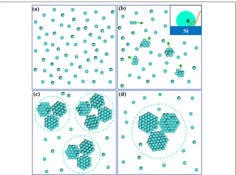
According to our previous study [28,29], the fabrica-tion mechanism of the nanoparticle array is suggested a vapor-solid process. First, ZnO molecules form the ther-mal chemical vapor transport of source deposit on the substrate and then thermally diffuse on surface. Second, many small ZnO clusters would form by ZnO molecules by ZnO molecules continuously diffusing and colliding as shown in Figure 5b. Then, these small ZnO clusters still thermally diffuse on the surface, because there is an immiscible-like interaction between ZnO cluster and Si surface. In the inset in Figure 5b, we can see that the contact angle between ZnO cluster and Si surface is about 110° [28-33]. Thus, this contact angle is so large that ZnO clusters could easily thermal diffuse on Si sur-face, which seems a driving force to push ZnO cluster moving on surface. Third, large ZnO clusters would form by small clusters continuously diffusing and collid-ing as shown in Figure 5c. Actually, the nucleation of ZnO could take place when the size of clusters reaches to that of the critical nucleus in this stage. Then, these small ZnO nuclei still thermally move on surface because of the immiscible-like interaction between ZnO cluster and Si surface. Finally, these particle constructed from small nuclei would stop moving on surface and grow up step by step when their size is sufficiently large as shown in Figure 5d. In other words, the large cluster will stand on surface when the immiscible-like interac-tion cannot provide sufficiently large driving force to push those big particles. In addition, Si surrounding ZnO QDs would be oxidized to form silicon oxides.
Figure 3The CL measurements of the ZnO nanoparticle array. SEM image (a), the panchromatic CL image (b), and the
corresponding CL spectrum (c).
0
2
4
6
8
10 12 14
3.2
3.4
3.6
3.8
4.0
4.2
4.4
4.6
4.8
5.0
Energy
(eV
)
Radius (nm)
2 4 6 8
240 280 320
wavelength (nm
[image:4.595.56.292.88.654.2]Radius (nm)
Thus, we can see that the ZnO nanoparticles are half-embedded in the amorphous silicon monoxide.
Conclusion
In summary, we have fabricated the ZnO nanoparticle array which is constructed from ZnO QDs on the Si substrate by the thermal chemical vapor transport and condensation without any metal catalysts. This fabri-cated ZnO nanostructure exhibited a great blue-shift of luminescence in the CL spectrum. These novel proper-ties show that the ZnO nanoparticle array has potential applications in UV emitters.
Abbreviations
CL: cathodoluminescence; EELS: electron-energy loss spectroscopy; FESEM: field emission scanning electron microscopy; QDs: quantum dots; TEM: transmission electron microscopy; UV: ultraviolet; XRD: X-ray diffraction.
Acknowledgements
This study was supported by the NSFC (U0734004) and the Ministry of Education.
Authors’contributions
N. W. Wang carried out the analysis and study of ZnO nanoparticle arrays, participated in the sequence alignment and drafted the manuscript. Y. H. Yang participated the luminescence analysis. G. W. Yang conceived of the study and participated in its design, coordination and the sequence alignment. All authors read and approved the final manuscript.
Competing interests
The authors declare that they have no competing interests.
Received: 11 March 2011 Accepted: 14 April 2011 Published: 14 April 2011
References
1. Huang MH, Mao S, Feick H, Yan HQ, Wu YY, Kind H, Weber E, Russo R, Yang PD:Room-temperature ultraviolet nanowire nanolasers.Science 2001,292:1897.
2. Heo YW, Norton DP, Tien LC, Kwon Y, Kang BS, Ren F, Pearton SJ, LaRoche JR:ZnO nanowire growth and devices.Mater Sci Eng R2004, 47:1.
3. Zeng HB, Duan GT, Li Y, Yang SK, Xu XX, Cai WP:Blue luminescence of ZnO nanoparticles based on non-equilibrium processes: defect origins and emission controls.Adv Funct Mater2010,20:561.
4. Yu H, Li JB, Loomis RA, Gibbons PC, Wang LW, Buhro WE:Cadmium selenide quantum wires and the transition from 3D to 2D confinement.
[image:5.595.61.539.86.440.2]J Am Chem Soc2003,125:16168.
Figure 5Schematic illustration of the fabrication mechanism of the ZnO nanoparticle array constructed from ZnO QDs. ZnO molecules randomly diffusing on surface (a), ZnO clusters thermally diffusing on surface and the inset showing the contact angleθ(b), large clusters formation by small clusters continuously diffusing and colliding (c), and big particles formation (d).
Wanget al.Nanoscale Research Letters2011,6:338 http://www.nanoscalereslett.com/content/6/1/338
6. Lin KF, Cheng HM, Hsu HC, Hsieh WF:Band gap engineering and spatial confinement of optical phonon in ZnO quantum dots.Appl Phys Lett 2006,88:263117.
7. Kim KK, Koguchi N, Ok YW, Seong TY, Park SJ:Fabrication of ZnO quantum dots embedded in an amorphous oxide layer.Appl Phys Lett 2004,84:3810.
8. Ko HJ, Chen YF, Yao T, Miyajima K, Yamamoto A, Goto T:Biexciton emission from high-quality ZnO films grown on epitaxial GaN by plasma-assisted molecular-beam epitaxy.Appl Phys Lett2000,77:537. 9. Kim SW, Fujita S, Fujita S:Self-organized ZnO quantum dots on SiO2/Si
substrates by metalorganic chemical vapor deposition.Appl Phys Lett 2002,81:5036.
10. Wang NW, Yang YH, Yang GW:Fabry-Pérot and whispering gallery modes enhanced luminescence from an individual hexagonal ZnO
nanocolumn.Appl Phys Lett2010,97:041917.
11. Yang SJ, Park CR:Facile preparation of monodisperse ZnO quantum dots with high quality photoluminescence characteristics.Nanotechnology 2008,19:035609.
12. Abdullah M, Shibamoto S, Okuyama K:Synthesis of ZnO/SiO2 nanocomposites emitting specific luminescence colors.Opt Mater2004, 26:95.
13. Cheng HM, Lin KF, Hsu HC, Hsieh WF:Size dependence of
photoluminescence and resonant Raman scattering from ZnO quantum dots.Appl Phys Lett2006,88:261909.
14. Giannakopoulos K, Boukos N, Travlos A, Monteiro T, Soares MJ, Peres M, Neves A, Carmo MC:Structural and photoluminescence properties of ZnO nanoparticles on silicon oxide.Appl Phys A -Mater2007,88:41. 15. Giannakopoulos K, Boukos N, Travlos A:Self-assembled zinc oxide
nanodots on silicon oxide.J Phys Conf Ser2005,10:121.
16. Giannakopoulos K, Boukos N, Travlos A:Zinc oxide nanoparticles on silicon.Superlattice Microstruct2006,39:115.
17. Sato Y, Mizoguchi T, Oba F, Yodogawa M, Yamamoto T, Ikuhara Y: Identification of native defects around grain boundary in Pr-doped ZnO bicrystal using electron energy loss spectroscopy and first-principles calculations.Appl Phys Lett2004,84:5311.
18. Zhang ZL, Su DS:Behaviour of TEM metal grids during in-situ heating experiments.Ultramicroscopy2009,109:766.
19. Wenger KS, Cornu D, Chassagneux F, Epicier T, Miele P:Direct synthesis of amorphous silicon dioxide nanowires and helical self-assembled nanostructures derived therefrom.J Mater Chem2003,13:3058. 20. Song M, Fukuda Y, Furuya K:Local chemical states and microstructure of
photoluminescent porous silicon studied by means of EELS and TEM. Micron2000,31:429.
21. Bonnet N, Brun N, Colliex C:Extracting information from sequences of spatially resolved EELS spectra using multivariate statistical analysis. Ultramicroscopy1999,77:97.
22. Lai YS, Wang JL, Liou SC, Tu CH:Size and density control of silicon oxide nanowires by rapid thermal annealing and their growth mechanism. Appl Phys A2009,94:357.
23. Schulmeister K, Mader W:TEM investigation on the structure of amorphous silicon monoxide.J Non-Cryst Solids2003,320:143. 24. Wang NW, Yang YH, Yang GW:Indium oxide-zinc oxide nanosized
heterostructure and whispering gallery mode luminescence emission.
J Phys Chem C2009,113:15480.
25. Aleksandra B, DjurišićDr, Leung YH:Optical properties of ZnO nanostructures.Small2006,2:944.
26. Kayanuma Y:Quantum-size effects of interacting electrons and holes in semiconductor microcrystals with spherical shape.Phys Rev B1988, 38:9797.
27. Lin B, Fu Z, Jia Y:Green luminescent center in undoped zinc oxide films deposited on silicon substrates.Appl Phys Lett2001,79:943.
28. Yang YH, Wang B, Yang GW:Mechanisms of self-catalyst growth of agave-like zinc oxide nanostructures on amorphous carbons.Cryst
Growth Des2007,7:1242.
29. Wang CX, Wang B, Yang YH, Yang GW:Thermodynamic and kinetic size limit of nanowire growth.J Phys Chem B2005,109:9966.
30. Givargizov EI:Highly Anisotropic Crystals.Boston, MA: D. Reidel; 1986.
L342.
33. Alivisatos AP:Semiconductor clusters, nanocrystals, and quantum dots. Science1996,271:933.
doi:10.1186/1556-276X-6-338
Cite this article as:Wanget al.:Great blue-shift of luminescence of ZnO
nanoparticle array constructed from ZnO quantum dots.Nanoscale Research Letters20116:338.
Submit your manuscript to a
journal and benefi t from:
7 Convenient online submission 7 Rigorous peer review
7 Immediate publication on acceptance 7 Open access: articles freely available online 7 High visibility within the fi eld
7 Retaining the copyright to your article