Design of Reversible Random Access Memory
Md. Selim Al Mamun
Department of Computer Science and Engineering, Jatiya Kabi Kazi Nazrul Islam University,
Bangladesh.
Syed Monowar Hossain
Department of Computer Science and Engineering, University of Dhaka
Bangladesh.
ABSTRACT
Reversible logic has become immensely popular research area and its applications have spread in various technologies for their low power consumption. In this paper we proposed an efficient design of random access memory using reversible logic. In the way of designing the reversible random access memory we proposed a reversible decoder and a write enable reversible master slave D flip-flop. All the reversible designs are superior in terms of quantum cost, delay and garbage outputs compared to the designs existing in literature.
General Terms
VLSI design, quantum computing, reconfigurable computing, fault-tolerant system.
Keywords
Flip-flops, Garbage Output, Random Access Memory, Reversible Logic, Quantum Cost.
1.
INTRODUCTION
In recent year reversible computing has emerged as a promising technology. The primary reason for this is the increasing demands for low power devices. R. Landauer [1] proved that losing information causes loss of energy. Information is lost when an input cannot be recovered from its output. He showed that each bit of information loss generates kTln2 joules of heat energy; where k is Boltzmann’s constant and T is the absolute temperature at which computation is performed. C. H. Bennett [2] showed that energy dissipation problem can be avoided if circuits are built using reversible logic gates.
In reversible logic there is a one to one mapping between its input and output. As a result no information bit is lost and no loss of energy [3]. Random Access Memory (RAM) uses bistable sequential circuitry to store a single bit. Although many researchers are working on reversible memory elements, little work has been done in this area. In current literature the number of reversible gates is used as a major metric of cost optimization [4]. Dmitri Maslov and Michael Miller [5] showed that number of gates is not a good metric of optimization as reversible gates are of different types and have different quantum costs. In this paper, we proposed a new design of RRAM that is efficient in terms of quantum cost, delay and the number of garbage outputs.
The rest of the paper is organized as follows: Section 2 presents some basic definitions related to reversible logic. Section 3 describes some popular reversible logic gates and their quantum representation. Section 4 describes our proposed modification on Frekdin gate (FRG). Section 5 describes the logic synthesis of RRAM and compares our
proposed design with other researchers. Finally this paper is concluded with Section 6.
2.
BASIC DEFINITIONS
In this section, some basic definitions related to reversible logic are presented. We formally define reversible gate, garbage output, delay and quantum cost in reversible circuits.
2.1. Reversible Gate
A Reversible Gate is a k-input and k-output (denoted by k*k) circuit that produces a unique output pattern for each possible input pattern [6]. If the input vector of the reversible gate is defined as Iv where Iv = (I1,j , I2,j , I3,j, …. , Ik-1,j , Ik,j) and
the output vector as Ov where Ov = (O1,j , O2,j , O3,j , … , Ok-1,j
, Ok,j), then according to the definition, for each particular
vector j, Iv Ov.
2.2. Garbage Output
Outputs that are not primary outputs or outputs that are not used as input to other gates to produce primary outputs are garbage. Unwanted or unused outputs which are needed to maintain reversibility of a reversible gate (or circuit) are known as Garbage Outputs. The garbage output of Feynman gate [7] is shown Figure 1 with *.
2.3. Delay
The delay of a logic circuit is the maximum number of gates in a path from any input line to any output line. The definition is based on two assumptions: (i) Every gate computation takes one unit of time and (ii) All inputs to the circuit are available before the computation. In this paper, we used the logical depth as measure of the delay proposed by Mohammadi and Eshghi [8]. The delay of each 1x1 gate and 2x2 reversible gate is taken as unit delay 1. Any 3x3 reversible gate can be designed from 1x1 reversible gates and 2x2 reversible gates, such as CNOT gate, Controlled-V and Controlled-V+ gates (V is a square-root-of NOT gate and V+ is its hermitian). Thus, the delay of a 3x3 reversible gate can be computed by calculating its logical depth when it is designed from smaller 1x1 and 2x2 reversible gates.
2.4. Quantum Cost
3.
QUANTUM ANALYSIS OF POPULAR
REVERSIBLE GATES
Every reversible gate can be realized by the quantum gates. Thus the cost of reversible circuit can be measured in terms of quantum cost. Reducing the quantum cost of a reversible circuit is always a challenging one and works are still going on in this area. This section describes some popular reversible gates and presents quantum equivalent diagram of each of the reversible gate.
3.1
Feynman Gate
The input vector Ivand output vector Ov of 2*2 Feynman gate
is defined as Iv = (A, B) and Ov = (P = A,QAB). The
quantum cost of Feynman gate is 1. The block diagram and equivalent quantum representation of 2*2 Feynman gate are shown in Fig. 1.
(a)
(b)
Fig. 1. (a) Block diagram of 2x2 Feynman gate and (b) Equivalent quantum representation
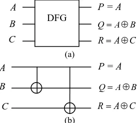
3.2
Double Feynman Gate
The input vector Iv and output vector Ov of 3*3 Double
Feynman gate (DFG) is defined as Iv = (A, B, C) and Ov = (P
= A,QAB,RAC). The quantum cost of Double Feynman gate is 2 [10]. The block diagram and equivalent quantum representation of 3*3 Double Feynman gate are shown in Fig. 2.
(a)
(b)
Fig. 2. (a) Block diagram of 3x3 Double Feynman gate and (b) Equivalent quantum representation.
3.3
Toffoli Gate
The input vector Ivand output vector Ovof 3*3 Toffoli gate
(TG) [11] is defined as Iv = (A, B, C) and Ov = (P = A, Q = B,
R = AB
C). The quantum cost of Toffoli gate is 5. The block diagram and equivalent quantum representation of 3*3 Toffoli gate are shown in Fig. 3.(a)
(b)
Fig.3. (a) Block diagram of 3*3 Toffoli gate and (b) Equivalent quantum representation.
3.4
Frekdin Gate
The input vector Ivand output vector Ovfor 3*3 Fredkin gate
(FRG) [12] is defined as follows: Iv = (A, B, C) and Ov =
(P=A, QABAC, RACAB). The quantum cost of Frekdin gate is 5. The block diagram and equivalent quantum representation of 3*3 Fredkin gate are shown in Fig. 4.
(a)
(b)
Fig.4. (a) Block diagram of 3*3 Frekdin gate and (b) Equivalent quantum representation.
3.5
Peres Gate
The input vector Ivand output vector Ov of 3*3 Peres gate
(PG)[13] is defined as follows: Iv = (A, B, C) and Ov = (P = A,
Q = A B, R = AB C). The quantum cost of Peres gate is 4. The block diagram and equivalent quantum representation of 3*3 Peres gate are shown in Fig. 5.
(a)
(b)
Fig.5. (a) Block diagram of 3*3 Peres and (b) Equivalent quantum representation.
V V V+
A
B
C
P = A
B A
Q
C AB
R
Peres Gate
A
B
C
P = A
B A
Q
C AB
R
V V+
V
A
B
C
P = A
AC B A
Q
AB C A
R
Frekdin Gate
A
B
C
P = A
AC B A
Q
AB C A
R
A
B
C
P = A
Q = B
C AB
R
V+ V
V
Toffoli Gate
A
B
C
P = A
Q = B
C AB
R
A
B
C
P = A
B A
Q
C A R
DFG
P = A
B A
Q
C A R A
B
C A
B
P=A*
B A
Q
Feynman Gate
A
B
P=A*
B A
[image:2.595.332.540.74.212.2] [image:2.595.105.240.271.391.2] [image:2.595.333.563.316.461.2] [image:2.595.97.235.508.631.2] [image:2.595.329.530.562.702.2]4. PROPOSED MODIFICATION ON
FREKDIN GATE
4.1 Modified FRG 1 gate
The input vector, Ivand output vector, Ovfor 3*3 modified
Fredkin Gate (MFRG1) is defined as follows: Iv = (A, B, C)
and Ov=(P=A,QABAC,RACAB). The quantum
[image:3.595.333.523.72.198.2]cost of MFRG1 gate is 4.
Fig. 6. Quantum representation of MFRG1 gate
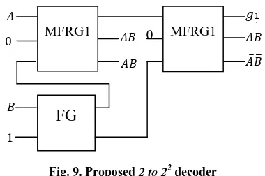
4.2 Modified FRG 2 gate
The input vector Ivand output vector Ovof 3*3 modified
Fredkin Gate (MFRG2) is defined as Iv = (A, B, C) and Ov = (
A
P , QABAC, RACAB). The quantum cost of MFRG2 gate is 5.
Fig. 7. Quantum representation of MFRG2 gate
5. DESIGN OF RANDOM ACCESS
MEMORY
In this section we first presented proposed design for all the components of RRAM. Then we presented our proposed novel design of RRAM that is optimized in terms of quantum cost, delay and garbage outputs.
[image:3.595.62.265.169.235.2]5.1. Proposed Reversible n to 2
nDecoder
A single Feynman gate can be used to design the basic 1 to 21 decoder. Using this decoder we can systematically add 2n-1 number of MRFG1 gates to the design to achieve n to 2n decoder. The design of 1 to 21 decoder is shown in Figure. 8.Fig. 8. Proposed 1 to 21 decoder
The design of decoder has 1 quantum cost, 1 delay and no garbage output.
Our proposed 2 to 24 decoder using MRFG1 gates are shown in Figure 9.
Fig. 9. Proposed 2 to 22 decoder
The proposed 2 to 22 decoder has quantum cost 9, delay 9 and bare minimum of 1 garbage bit. The proposed design of 2 to 22 decoder achieves improvement ratios of 18%, 18% and 50% in terms of quantum cost, delay and garbage outputs compared to the design presented in N.M.Nayeem et al. [14]. The improvement ratios compared to the design M. Morrison et al. presented in [19] are 10% and 10% in terms of quantum cost and delay. The comparison of proposed 2 to 22 decoder with the existing ones shown in table I.
Table I. Comparison of different types of 2 to 22 decoders.
2 to 22 decoder design
Cost Comparisons Quantum
Cost
Delay Garbage Outputs Proposed 9 9 1
Existing[14] 11 11 2
Existing[19] 10 10 -
Improvement(%) w.r.t. [14] 18 18 50
Improvement(%) w.r.t. [19] 10 10 -
Theorem 1: To construct n to 2n decoder, if g is the total number of gates required to design the decoder producing b number of garbage outputs then g ≥ 2n
-1 and b ≥ n-1.
Proof: For 1 to 21 decoder only one Feynman gate needed that doesn’t produce any garbage bit. So number of gate = 1 and garbage output = 0.
Now for n>1, n to 2n decoder design requires that each of the output of the (n-1) to 2(n-1) decoders together with (n-1) selection bits are employed in separate MRFG1 gate to produce selections for n to 2n decoder. In that case overall number of gates becomes 2n-1, because for n=1 we were required only 1 gate. This design has n-1 garbage bits as the 1 to 21 decoder produces zero garbage.
Theorem 2: The quantum cost of an n to 2n decoder is Qc ≥
4.2n-7.
Proof: From theorem 1, at least 2n-1 gates are required to design n to 2n decoder. For n = 1 only one 2*2 Feynman gate
is required which has quantum cost 1. Then 2n-2 MRFG1 gates are required and each MRF1 gate’s quantum cost is 4. So total quantum cost Qc is = (2n-2)4 +1 = 4.2n-7.
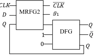
5.2. Proposed Single bit Memory Cell
The heart of our proposed memory block is D flip-flop. The characteristic equation of gated D flip-flop is Q+ = .D+ .Q. The D flip-flop can be realized by one MFRG2 gate and one FG. It can be mapped with MFRG2 by giving CLK , D and Q respectively in 1st, 2nd and 3rd inputs of
0
̅
MFRG1
̅
̅ ̅ MFRG1
FG
Feynman Gate A
A 1
A
V V V+
A
C
B QABAC
AB C A
R
A P
V V V+
A
B
C
C A B A
Q
P = A
AB C A
[image:3.595.110.214.531.589.2]MFRG2 gate. The Figure 10 shows our proposed D flip-flop with and ̅ outputs.
Fig. 10: Proposed design of D flip-flop with and ̅ outputs.
[image:4.595.311.549.212.296.2]The proposed D flip-flop with and ̅ outputs has quantum cost 7, delay 7 and has the bare minimum of 1 garbage bit. The proposed design of gated D flip-flop achieves improvement ratios of 50% in terms of garbage outputs compared to the design presented in Thapliyal et al. 2010[15] and L. Jamal et al. 2012[16]. The comparisons of our D flip-flop (with and ̅ outputs) design with existing designs in literature are summarized in Table II.
Table II. Comparison of different types of D flip-flops with and ̅ outputs.
D flip-flop design Quantum Cost Comparisons Cost
Delay Garbage Outputs Proposed 7 7 1
Existing[15] 7 7 2
Existing[16] 7 7 2
Improvement(%) w.r.t. [15] 0 0 50
Improvement(%) w.r.t. [16] 0 0 50
[image:4.595.52.290.344.456.2]We need Write Enable Master Slave D FFs to design a Reversible Random Access Memory (RRAM). Our proposed write enable master slave flip-flop is shown in Figure 11.
Fig. 11: Proposed write enable master slave D flip-flop.
As data are both read from and written into RAM, each Flip-Flop should work on two modes- read and write. A MFRG1 gate is used to multiplex between flip-flop’s D input and stored bit Q in the flip-flop. When ‘write’ is high, input D of
the MRFG1 gate is carried to the first D flip-flop and if ‘write’ is low, output of the D flip-flop is fed back to the second input of the MRFG1 gate so that state of the flip-flop remains same.
The proposed write enable master slave D flip-flop has quantum cost 17, delay 17 and 3 garbage bits. The proposed design of single bit memory cell achieves improvement ratios of 19% and 11% in terms of quantum cost and delay compared to the design presented in M. Morrison [19]. The comparisons are summarized in table III.
Table III. Comparisons of different types of Write Enable Master Slave D flip-flops with and ̅ outputs.
Single bit Memory Cell
Cost Comparisons Quantum
Cost
Delay Garbage Outputs Proposed 17 17 3
Existing[19] 21 19 -
Improvement in (%) 19 11 -
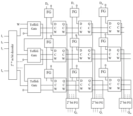
5.3. Proposed Reversible Random Access
Memory (RRAM)
A RAM is a two dimensional array of flip-flops. There are 2n rows where each row contains m flip-flops. Each time only one of the 2noutput lines of the decoder is active which selects one row of flip-flops of the RAM. Whether a read or a write operation is performed depends on the W input. When W is high, m flip-flops of the selected row of the RAM are written with the inputs D1 to Dm. When W is low, Q1 to Qm
contains stored bits in the flip-flops of the selected row and simultaneously the flip-flops are refreshed with the stored bits. The proposed design of 2n *m bit RRAM is shown in Figure.12.
Theorem 3
Let g be the number of gates required to realize a 2n* m Reversible RAM where n be the number of bits and m be the selection bits in the RRAM, then g ≥2n *(6m+2) +m-1.
Proof: A 2n * m RRAM requires n to2n decoder that consists of (2n-1) gates. 2n Toffoli gates are required to perform AND
operations in RRAM. m*2n D flip-flops are required inside the m * 2nRRAM whereas each D flip-flop requires 5 gates. 2n * m Feynman gates are required to perform the copy operation. There are m number of 2n bit Feynman gate at the blottom last row. If g be the minimum number of gates to realize the RRAM, then g≥(2n
-1) + 2n + 5*2n*m + 2n*m+m Hence g ≥ 2n
*(6m+2)+m -1.
Theorem 4
Let n be the number of bits, m be the selection bits in the RRAM and b be the number of garbage outputs generated from the RRAM, then b≥ m*(4.2n -1)+n.
Proof: A 2n * m RRAM requires n to2n decoder which produces (n-1) garbage bits. 1 garbage bit is generated from the mth Toffoli gate in the RRAM. Inside RRAM there are 2n*m D flip-flops and each D flip-flop produces 3 garbage bits. The last row contains m number of 2n bit Feynman gate and each of them produces 2n-1garbage bits. If b be the
number of garbage outputs then b ≥(n-1) + 1 + 3*2n*m + m*(2n-1).
Hence b ≥ m*(4.2n
-1) + n.
g2
0
FG
CLK
MFRG1 W
D
Q
W ̅̅̅̅̅̅
DFG
QMFRG2 CLK
g1
g3
MFRG2
̅
̅̅̅̅̅̅
[image:4.595.59.284.516.694.2]Fig.12. Proposed design of 2n * m bit RRAM
Theorem 5
Let n be the number of bits, m be the selection bits in the RRAM and Qc be the quantum cost of the RRAM, then Qc≥ 2n
(19m+9)-7.
Proof: A 2n * m RRAM requires an n to2n decoders that has quantum cost 4.2n-7. 2n Toffoli gates are used to perform AND operations in RRAM where each of the gates has quantum cost 5, m*2n DFFs are required inside the m * 2n RRAM whereas each DFF has quantum cost 17. 2n * m Feynman gates are required to perform the copy operation where each of them has quatum cost 1. There are m number of 2n bit Feynman gate in last row where each of them has
quantum cost 2n. If Qc be the quantum cost of RRAM then Qc≥ 4.2n-7 +5.2n+ m*2n+17*m*2n+ m*2n.
Hence Qc≥ 2n(19m+9)-7
6. CONCLUSION
Reversible Random Access Memory (RRAM) is going to take the place of existing main memory in the forthcoming quantum devices. In this paper we proposed optimized RRAM with the help of proposed MRFG1 and MRFG2 gates along with some basic reversible logic gates. Appropriate algorithms and theorems are presented here to clarify the proposed design and to establish its efficiency. We compare our design with existing ones in literature which claims our success in terms
of quantum cost, number of garbage outputs and delay. We believe this optimization can contribute significantly in reversible logic community.
7. ACKNOWLEDGMENTS
The authors would like to thank the anonymous referees for their constructive feedback, which helped significantly improving technical quality of this paper.
8. REFERENCES
[1] Rolf Landauer, "Irreversibility and Heat Generation in the Computing Process", IBM Journal of Research and Development, vol. 5, pp. 183-191, 1961.
[2] Charles H.Bennett, "Logical Reversibility of computation", IBM Journal of Research and Development, vol. 17, no. 6, pp. 525-532, 1973.
[3] Perkowski, M., A.Al-Rabadi, P. Kerntopf, A. Buller, M. Chrzanowska-Jeske, A. Mishchenko, M. Azad Khan, A. Coppola, S. Yanushkevich, V. Shmerko and L. Jozwiak, “A general decomposition for reversible logic”, Proc. RM’2001, Starkville, pp: 119-138, 2001
[4] J.E Rice, "A New Look at Reversible Memory Elements", Proceedings International Symposium on
Dm
FG
0
0
0
0
D Q C C W W
D Q C C W W
FG
0
FG
0
2
n *
m
b
it d
ec
o
d
er
I1
I2
I3
In
D Q C C W W D Q C C W W
2n bit FG 2n bit FG 2n bit FG
Q0 Q1 Qm
D Q C C W W
D Q C C W W
D Q C C W W Toffoli
Gate
D Q C C W W Toffoli
Gate
D Q C C W W Toffoli
Gate
0
FG
FG
FG
0
0 D1
FG
FG
FG
0
0 D0
Circuits and Systems(ISCAS) 2006, Kos, Greece, May 21-24 ,2006, pp. 243-246.
[5] Dmitri Maslov and D. Michael Miller, “Comparison of the cost metrics for reversible and quantum logic synthesis”, http://arxiv.org/abs/quant-ph/0511008, 2006
[6] Hafiz Md.Hasan Babu, Md.Rafiqul Islam, Ahsan Raja Chowdhury, and Syed Mostahed Ali Chowdhury, "Synthesis of full-adder circuit using reversible logic," International Conference on VLSI Design, vol. 17, pp. 757-760, 2004.
[7] Richard P.Feynman, "Quantum mechanical computers," Foundations of Physics, vol. 16, no. 6, pp. 507-531, 1986.
[8] Mohammadi,M. and Mshghi,M, On figures ofmerit in reversible and quantumlogic designs, Quantum Inform. Process. 8, 4, 297–318, 2009.
[9] D. Michael Miller, Dmitri Maslov, GerhardW. Dueck, A Transformation Based Algorithm for Reversible Logic Synthesis, Annual ACM IEEE Design Automation Conference,Proceedings of the 40th annual Design Automation Conference, Anaheim, CA, USA Pages: 318 – 323.
[10]Perkowski, M., “A hierarchical approach to computer-aided design of quantum circuits”, 6th International Symposium on Representations and Methodology of Future Computing Technology, 201-209, 2003.
[11]Tommaso Toffoli, "Reversible Computing," Automata, Languages and Programming, 7th Colloquium of Lecture Notes in Computer Science, vol. 85, pp. 632-644, 1980. [12]Edward Fredkin and Tommaso Toffoli, "Conservative
Logic," International Journal of Theoretical Physics, vol. 21, pp. 219-253, 1982.
[13]A. Peres, "Reversible Logic and Quantum Computers," Physical Review A, vol. 32, pp. 3266-3276, 1985. [14]Sk. Noor Mahammad and Kamakoti Veezhinathan,
“Constructing Online Testable Circuits Using Reversible Logic”, Ieee transactions on instrumentation and measurement, vol. 59, no. 1, January 2010.
[15]Himanshu Thapliyal and Nagarajan Ranganathan, Design of Reversible Sequential Circuits Optimizing Quantum Cost, Delay, and Garbage Outputs, ACMJournal onEmerging Technologies inComputer Systems,Vol. 6,No. 4,Article 14, Pub. date:December 2010.
[16]Lafifa Jamal, Farah Sharmin, Md. Abdul Mottalib and Hafiz Md. Hasan Babu, Design and Minimization of Reversible Circuits for a Data Acquisition and Storage System, International Journal of Engineering and Technology Volume 2 No. 1, January, 2012
[17]H. Thapliyal and A. P. Vinod, “Design of reversible sequential elements with feasibility of transistor implementation” In Proc. the 2007 IEEE Intl. Symp. On Cir.and Sys., pages 625–628, New Orleans, USA, May 2007.
[18]M.-L. Chuang and C.-Y. Wang, “Synthesis of reversible sequential elements,” ACM journal of Engineering Technologies in Computing Systems (JETC). Vol. 3, No.4, 1–19, 2008.