2018 2nd International Conference on Modeling, Simulation and Optimization Technologies and Applications (MSOTA 2018) ISBN: 978-1-60595-594-0
Analysis and Test of Time Difference Measurement IP Based on FIB
Jun DENG
1,2,*, Ke-liu HU
1, Tao ZHANG
1, Hao LUO
1and Kun HUANG
11
Sichuan Institute of Solid-state Circuits, Chongqing, 400060, China
2
School of Microelectronics and Communication Engineering, Chongqing University, 400044, China
*Corresponding author
Keywords: IC Test, leakage current, FIB (Focused Ion Beam), Verification.
Abstract. With the development of semiconductor technology, how to locate and verify the problems found in chip testing becomes the key of the chip design. In the test of time difference measurement IP chip, test results find that the phase shift output does not correspond with the design requirements. After analyzing the circuit, the leakage current of refresh circuit is found. The FIB (Focused Ion Beam) technology is adopted to modify the physical circuit. The circuit is tested after FIB. The result shows that the judgement and analysis of the crux of the problem is correct. Through FIB, not only the problem is found, but also the function and performance of the chip are tested rapidly. The purpose of rapid verification is achieved, and the modification time is saved. Using FIB can help to reduce the cost of chip design sometimes.
Introduction
With the development of semiconductor technology, the scale and integration degree of semiconductor integrated circuit (IC) are increasing, and the complexity also increases, which make the designing and verification of IC more difficult, however the market time requires shorter. In an actual IC project, maybe we have resolved all problems during design and simulation, but some faults may appear when we test the IC, which are produced by foundry. This fatal result will influence on the market time of the products. In response to this situation, firstly we need to analysis the circuits of the IC and locate the sticking point, then we must verify the analysis results from physical circuits. In order to reduce time consumption and save research costs, a typical way of physical verification is the FIB (Focused Ion Beam) technology. FIB is that the ion beam produced by liquid metal ion source is accelerated by ion gun, and then focused on the sample. The surface produces a secondary electron signal to obtain an electron image, or a strong current ion beam is used to strip the surface atoms to complete the micro and nano surface processing, selective stripping of metal, silicon oxide or deposited metal layer. FIB is mainly used for the modifications of chip circuits. FIB technology can help designer to verify the design faster and more accurate, and adopting FIB to modify the chip can reduce the number of unsuccessful design changes and producing, shorten the R & D time and cycle [1].
In this paper, when testing the Time Difference Measurement (TDM) IP, the output result of Phase Shift (PS) is not our desire. Through analysis the circuits of the phase shift, we find the reason maybe the leakage current of the dynamic refresh circuit. So we need to adopt the FIB technology to modify the physical circuit of PS to verify the problem location [2].
Introduction of Time Difference Measurement IP
signal and the reference signal in phase, the PS unit includes delay line, refresh circuit and inventor. The TDC can convert high-precision time/phase information into digital output, which can handle the time interval between two asynchronous signals. The Controller unit provides controlling logic signals[1-3].
TDC Controller
Delay line Refresh Circuit
F1_1Hz
ONEPPS
[image:2.595.99.505.131.267.2]FO_OUT Shift Phase
Figure 1. The Structure of Time Difference Measurement IP.
Test and Analysis
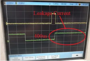
When testing the output of PS unit, the test results on the oscilloscope show that the output signal ‘FO_1Hz’ of PS is a periodic signal with a low level of about 440 µs. According to the design requirements, the signal should be a periodic signal of high level 30ms. It seems that the output is inverting. As shown in the following figure 2.
[image:2.595.206.389.443.568.2]By analyzing the circuit of PS unit, it is found that the refresh time of the dynamic Refresh Circuit is too short. In the ‘1s’ signal cycle, the leakage current of the device causes the holding time of the high level voltage to be only about 400 µs after ‘rstn’, so the high level state could not be maintained beyond that time.
Figure 2. Output waveform of Refresh Circuit unit.
The complete schematic diagram of Phase Shift is shown in the following figure 3.
(a) The complete schematic of Phase Shift
(c) The right half of the schematic Figure 3. Schematic of Phase Shift.
[image:3.595.117.478.417.490.2]The operating principle is that when PS unit is powered up and reset, the low level of rstn changes from low to high after a period of time, while the initial states of phase shift control code VC < 33:0 > and the delay chain output f < 33:0 > are all zero, and the NMOS transistors below are turned off. Therefore, PMOS charger PM0 increases the X potential of the input node of inverter I107 to VDD of the supply voltage, while the phase shift output signal f1out is 0. When a certain VC and f are equal to 1, the corresponding NMOS transistor pulls the node X potential down, so the output of phase shift ‘f1out’ becomes high level, after the high level lasts for 30ms, the rstn becomes low level, and the f1out output is pulled down again, thus obtaining the output of PS unit with a 30ms high-level. As can be seen from the following figure 4, the rstn of the PS unit is actually from the logical AND of the tow signals, which is the system reset signal rstn and the level control signal HALF1HZ output from the digital part. RSTN becomes high after holding low levels for a short period of time during power-on reset, so the output of the PS unit is actually controlled by HALF1HZ. According to the design of the digital part, the initial level of HALF1HZ is high, and it is pulled down when the PS generates a high-level output of 30ms, and then becomes high. HALF1HZ changes every 1s cycle.
Figure 4. Schematic of reset logical.
According to this principle, the leakage-substrate reverse PN junction leakage current of 35 NMOS transistors (NM0~NM34) will slowly discharge the X-node to 0 when the signal cycle time is very long, which corresponds to about 440 us in the measurement.
Verification by FIB
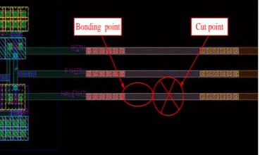
In order to verify the correctness for the analysis of the above problem, and to modify this fault to realize the quick test of the time difference measurement function, FIB can solve this problem. Firstly we need to cut off the level control signal HALF1HZ at the cut point as figure 5, then we need to grow a bonding point to connect the signal HALF1HZ, as shown in figure 6. Then A PAD will be made to connect with the bonding point, which will be connected to the pin on the tube.
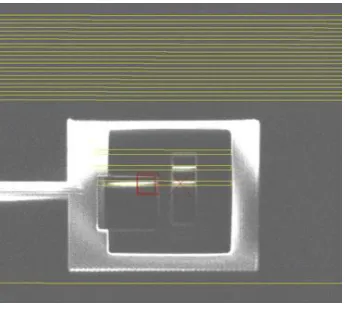
[image:3.595.206.391.671.781.2]Figure 6. The FIB image.
[image:4.595.200.397.390.531.2]After FIB, we need to test the correctness of this plan. On the test platform, the PAD produced by FIB will be injected into the excitation signal HALF1HZ by probe insertion, as showed in figure 7. The source signal come from of FPGA. The time sequence of HALF1HZ will be changed from low-pulling to high-pulling at the moment before the rising edge of the phase shift input signal F1_1HZ arrives, and then pull down after maintaining a high level of 30ms. It will be switched from charging state to maintaining the high level state. This interval is controlled within 10 us, which can avoid the change caused by the end of the discharge that the phase shift output becomes a high level. After the phase shift is completed, the HALF1HZ signal will be restored to low level and the refresh circuit will be charged continuously to maintain the low level state of phase shifting output. The test results are detailed in figure 8.
Figure 7. The test platform after FIB.
Figure 8. The test results after FIB.
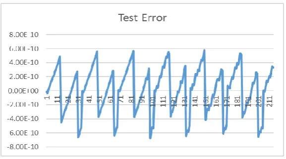
[image:4.595.199.398.395.670.2]Figure 9. Test error result.
Summary
In this paper, when testing TDM IP, the PS output does not correspond with the design requirements. Through analysis the circuits of PS, the leakage current of refresh circuit is found. The FIB is adopted to modify the physical circuit. The result shows that the judgement and analysis of the crux of the problem is correct. Through FIB, the purpose of rapid verification is achieved, and the modification time is saved, FIB can help to reduce the cost of chip design sometimes.
References
[1] XD Jiang, XH Yu, TR. Lundquist. Debug of IC-card chips assisted by FIB and in-situ mechanical microprobing, International Symposium on Optoelectonics & Microelectronics, 4600(2001)148-153.
[2] JC Reiner, P Gasser, U Sennhauser. Novel FIB-based sample preparation technique for TEM analysis of ultra-thin gate oxide breakdown. Microelectronics Reliability, 2002, 42 (9):1753-1757.
[3] C.S.Hwang, P.Chen, H.W.Tsao, A high-precision time-to-digital converter using a two-level conversion scheme, IEEE Trans. Nucl. Sci., vol. 51, No. 4, pp. 1349 (2004).
[4] B.K.Swann, B.J.Blalock, L.G.Clonts, et al, A 100-ps time-resolution CMOS time-to-digital converter for positron emission tomography imaging applications, IEEE J. Solid-State Circuits, vol. 39, No. 11, pp. 1839 (2004).