© 2015, IRJET ISO 9001:2008 Certified Journal
Page 485
A NOVEL METHOD TO IMPROVE THE PERFORMANCE OF DSTATCOM
USING DEADBEAT PREDICTIVE CONTROL ALGORITHM
M.Muthukumar
1, T.Venkatesan
21
PG student, Department of Electrical and Electronics Engineering, K.S.Rangasamy College of Technology,
Tamil Nadu, India
2
Professor, Department of Electrical and Electronics Engineering, K.S.Rangasamy College of Technology,
Tamil Nadu, India
---Abstract
-
In modern power system, the switching devices are generally used in combination with unbalanced reactive loads which produces current related Power Quality (PQ) problems by making source currents distorted and unbalanced. Usually a STATCOM is installed to support electricity networks that have a poor power factor and often poor voltage regulation. A Distribution Static Compensator (DSTATCOM) operating in Current Control Mode (CCM) is used to mitigate current related PQ problems. The main objective is to improve the performance of interactive distribution static compensator for address limitations of conventional Current Control Mode (CCM) and Voltage Control Mode (VCM) operations. In CCM operation, theDSTATCOM supplies reactive and harmonic
component of load currents to make source currents balanced, sinusoidal, and in-phase with respective phase load voltages In the previous research, the compensator with three single-phase H-bridge Voltage Source Inverters (VSIs), driven by a single DC storage capacitor was used and passive filter capacitor is also used to provide the path for high frequency components for current. Thus the operation and control of the improved performance interactive DSTATCOM is proposed for the continuous and stable load operation. Using the control algorithm, the range of source voltage within which a DSTATCOM should operate in CCM is computed. The advantage of the proposed is that the algorithm depends upon the supply voltage, maximum and minimum feeder impedance and load current. Outside this range, operational mode of DSTATCOM is transferred to VCM. Losses in feeder and VSI are reduced which improves efficiency of the system. The proposed method is implemented in MATLAB/simulink and shows that the performance is improved with reduced loss, cost, and power rating VSI as compared to the conventional CCM and VCM DSTATCOM operation.
Key Words:
Distribution Static Compensator
(DSTATCOM),
conventional Current Control Mode (CCM),Voltage Control Mode (VCM), Deadbeat predictive control algorithms
1. INTRODUCTION
Switching devices in combination with unbalanced reactive loads produce current related power quality (PQ) problems by making source currents distorted and unbalanced [1], [2]. A distribution static compensator (DSTATCOM) operating in current control mode (CCM) is used to mitigate current related PQ problems [3]–[9]. In CCM operation, the DSTATCOM supplies reactive and harmonic component of load currents to make source currents balanced, sinusoidal, and in-phase with respective phase load voltages
Generally, faults in power system and energization of larger loads create voltage disturbances like sag and swell. Also, integration of intermittent distributed generation causes voltage fluctuations in the distribution system. These voltage disturbances significantly affect the power transfer from the source to load and degrade the performance of sensitive loads [10]. However, conventional CCM operation of DSTATCOM cannot improve the load voltage. This is major limitation of CCM operation of DSTATCOM which considerably restricts its utilization. A DSTATCOM, when operated in voltage control mode (VCM), is one of the most effective device used for load voltage regulation [10]–[14]. In VCM operation, the DSTATCOM regulates load voltage at a constant reference value by supplying appropriate fundamental reactive current into the source.
© 2015, IRJET ISO 9001:2008 Certified Journal
Page 486
operation of DSTATCOM is not required during normalsupply conditions. Aforementioned analysis brings the fact that the conven- tional CCM and VCM operations of DSTATCOM are not required during voltage disturbances and normal disturbances, respectively.
[image:2.595.325.556.416.591.2]This greatly limits utilization of the DSTATCOM. Moreover, recent advancements in device topologies and con- trol algorithms have encouraged customers to look for devices which can provide various operational characteristics with less number of components, reduced cost, weight, and space This paper proposes operation and control of an improved performance interactive DSTATCOM for continuous and sta- ble load operation while addressing aforementioned issues. In this work, a control algorithm is proposed to compute range of source voltage within which a DSTATCOM should operate in CCM. This algorithm depends upon the supply voltage, maximum and minimum feeder impedance, and load current. Outside this range, operational mode of DSTATCOM is transferred to VCM. This interactive DSTATCOM pro- vides several operational features which are not possible in conventional DSTATCOM operation i.e., 1) Advantages of CCM during normal supply conditions, 2) Advantages of VCM during voltage disturbances, 3) Unlike conventional VCM, no reactive power exchanges with the supply during normal supply conditions, 4) Reduced losses in VSI and feeder compared to conventional VCM, and 5) Requires reduced rating VSI for sag mitigation compared to conventional VCM.
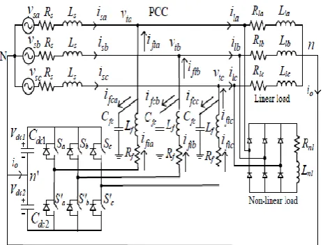
Fig-1-Three phase circuit of DSTATCOM in a distribution system.
2. DSTATCOM STRUCTURE AND CONTROLLER
DESIGN IN CCM AND VCM
Fig. 1 shows the power circuit diagram of a DSTATCOM connected at point of common coupling (PCC). It is realized by a three-phase, four-wire VSI with two dc link capacitors [11]. An LC filter is connected between the VSI and PCC. Shunt capacitor, Cfc, connected across PCC helps in elimi- nation of high-switching frequency components and prohibits them to enter into the source. Voltages across both the dc capacitors Cdc1 = Cdc2 = Cdc are maintained at a constant value Vdc1 = Vdc2 = Vdc. Source voltages, PCC voltages, load currents, source currents, and filter currents are vsj, vlj, ilj, isj, and iftj, respectively with j = a, b, c as three phases.
2.1
System Modeling and Development of
Switching Strategy
The VSI topology used in this work provides an independent control of each leg of the VSI [17]. This makes modelling of single phase circuit shown in Fig. 2 sufficient to explain the operation. Output voltage of the VSI is represented by uVdc. The term, u, is a switching control variable (with value +1 or -1). State space equation for this circuit is given as follows:
(1)
[image:2.595.45.277.475.651.2](2)
Fig-2 Single Phase Equivalent Circuit of DSTATCOM
2.2 Generation of Current Control Law:
The filter current at the (k+1)th sampling instant, from (2), is given as following:
(3)
© 2015, IRJET ISO 9001:2008 Certified Journal
Page 487
IGBT which is unknown at the kth sampling. Therefore, acost function (J) is defined as follows
(4)
Where fi(k + 1) is reference current at (k + 1)th sampling. To minimize cost function, it is differentiated with respect to ui(k) and equated to zero. Finally, J is minimum at Reference current control law is obtained after replacing.
However, it can be noticed that the contains future reference current I fi
(k + 1) which is unknown. To know the future value of any signal in discrete domain when sampling time is constant, extrapolation is used which predicts the future value using known values of previous sampling instants. Order of extrapolation depends upon the sampling period. Lesser the sampling period, higher will be extrapolation and vice versa. To know i_ f i(k+1), following Lagrange’s extrapolation formula
(5)
Reference current control law is obtained after replacing (5) in (3). However, it can be noticed that the contains future reference current i f i(k + 1) which is unknown. To know the future value of any signal in discrete domain when sampling time is constant, extrapolation is used which predicts the future value using known values of previous sampling instants. Order of extrapolation depends upon the sampling period. Lesser the sampling period, higher will be extrapolation and vice versa. To know i fi(k+1), following Lagrange’s extrapolation formula is used
(6)
(7)
Expression for reference current, i fi(k + 1), is valid for a wide frequency range, when substituted in (3) yields to onestep- ahead deadbeat current control law. The reference current control law from (3), (5), and (7) is given as
)
2.3 Generation of Voltage Control Law
From (2), the capacitor voltage at the
k + 1th sampling instant will be
(9)
The reference control laws, u_ i (k) and u_ v (k), are converted into corresponding VSI switching commands using deadbeat current and voltage controller, respectively . The deadbeat predictive control scheme provides stable and robust operation of the system with excellent dynamic performance. The stability of the system can be verified by applying the z transform, where the transfer function of system in z domain is given as follow
(12)
In the above transfer function, all the components of the matrices G and H are known. Also, the term I represents unit matrix. Now, the stability of the deadbeat predictive control scheme is found by analysing the poles of the above transfer function. It is found that all the poles of the transfer function lie within the unit circle. Therefore, the scheme used in this work satisfies the stability criterion
3. CONTROL OF DC LINK VOLTAGE
The DSTATCOM remains operational without taking any
real power from the Type equation here.source.
However, dc link voltage decreases continuously due to the losses in the inverter. Therefore, a control loop is required to maintain the capacitor voltage at a reference value by compensating its losses. It is achieved by taking small real power from the source. The capacitor voltage control in CCM and VCM is achieved as following
3.1 Control of Dc Link Voltage in CCM:
© 2015, IRJET ISO 9001:2008 Certified Journal
Page 488
dc link voltage constant. These are computed using aProportional Integral (PI) controller at positive zero crossing of phase-a voltage. It helps in maintaining the dc link voltage (vdc1 + vdc2) ata predefined reference value by drawing a set of balanced currents from the source and is given as
Where Kpc, Kic, and evdc = 2 Vdcref - (vdc1 +
vdc2) are proportional gain, integral gain, and
voltage error of the PI controller, respectively.
3.2 Control of Dc Link Voltage in Vcm:
Average real power at the PCC (Ppcc) is sum of average load power and VSI losses (Ploss). The power, Ppccis taken from the source depending upon the angle between source and load voltages i.e., load angle. The VSI losses are compensated by taking small real power, Ploss, from the source.
If capacitor voltage is regulated to a reference value, then in steady state condition Ploss is a constant value and forms a fraction of Ppcc. Thus is also a constant value. Once operation mode of DSTATCOM is transferred to VCM, dc link voltage is regulated by generating a suitable value of. The total dclink voltage (vdc1 + vdc2) is compared with a reference voltage and error is passed through a PI controller. Output of the PI controller, is given as
(13)
Where Kpvand Kiv are proportional and integral gains of the PI controller, respectively. For stable operation, the value of must lie from 0 to 90 degree. Consequently, controller gains are quite small and are chosen carefully.
4. FLEXIBLE MODE TRANSFER VOLTAGE
RANGE FOR INTERACTIVE DSTATCOM
Generally, loads perform satisfactorily within the 10% range of the nominal voltage (i.e., 0.9 to 1.1 p.u.)also called normal operating conditions. In these conditions, current related PQ problems are of the main concern. Therefore the DSTATCOM is operated in CCM for load harmonic and reactive current compensation. It results in balanced and sinusoidal source currents with unity power factor at the PCC. However, the load voltage can change at any time due to voltage disturbances.
This will result in performance deterioration of the sensitive loads making CCM operation of DSTATCOM redundant. In this case, DSTATCOM must switch to VCM from CCM to protect sensitive loads from these unwanted variations in voltage by maintaining a constant voltage at the load terminal. In this section, a control algorithm for flexible mode transfer between CCM to VCM and vice versa has been presented. At any time of DSTATCOM operation, relation between the source and load points is given as follows:
(14)
The DSTATCOM operating in CCM maintains unity power factor at the PCC. Therefore, the source current and the load voltage will be in-phase with the each other. Vs\_ = VT + IsRs + jIsXs
(15)
It is clear that the minimum source voltage at which the load voltage does not become less than 0.9 p.u. must be computed at the base value of the feeder impedance. If load voltage is more than 0.9 p.u. for maximum load then it will certainly be more than 0.9 p.u. for other loads. Also, it is required to find out minimum operating source voltage at which the load voltage will be more than 1.1 p.u. of the nominal voltage. The load experiences voltage swell. If load voltage is less than 1.1 p.u. for the lowest possible value of the load power, then it is valid for all other loads. Even though this scheme does not require knowledge of source impedance throughout the DSTATCOM operation several schemes for online grid impedance measurement have been available
4.1 Control Block Diagram of Proposed
Interactive Dstatcom.
The power circuit diagram of a DSTATCOM connected at point of common coupling. It is realized by a three-phase, four wire VSI with two dc link capacitors. An LC filter is connected between the VSI and PCC Usually a STATCOM is installed to support electricity networks that have a poor power factor and often poor voltage regulation.
© 2015, IRJET ISO 9001:2008 Certified Journal
Page 489
The controller of the DSTATCOM is used to operate theinverter in such a way that the phase angle between the
inverter voltage and the line
voltage is dynamically
adjusted so that the DSTATCOM generates or
absorbs the desired VAR at the point of
connection.
Fig-3: Control Block Diagram of proposed Interactive
DSTATCOM
.
If Vi is equal to Vs, the reactive power is zero and the DSTATCOM does not generate or absorb reactive power. When Vi is greater than Vs, the DSTATCOM 'sees' an inductive reactance connected at its terminal
5. SIMULATION AND RESULTS
Improved performance interactive DSTATCOM, results providing limitations of the conventional CCM and VCM DSTATCOM operations are presented. PSCAD software is used for the simulation studies. Systemparameters Performance of conventional CCM operation of DSTATCOM . Throughout the operation, filter current consists of reactive and harmonic component of load current and makes source current sinusoidal and in-phase with the load voltage. For t =0.4 to 0.6 s, source voltage is reduced by 30%.
5.1 Simulation Results with Conventional
VEM.
In waveforms of conventional VCM operation of DSTATCOM where reference voltage is set at 1.0 p.u.Here the DSTATCOM compensates for the drop in the feeder. In this case, filter supplies reactive current into the source, and source current leads the load voltage. Therefore, filter and source currents are increased.
Compensation performance of proposed interactive DSTATCOM operation. Nominal source voltage is applied for t = 0 to 0.4 s. The DSTATCOM operates in CCM to compensate for load harmonic and reactive current. The load voltage and source current are sinusoidal.
The filter current, consisting of harmonic and reactive components of load current, makes the load voltage and source current in- phase with each other. Also, source
does not exchange reactive power as opposed to 4
kVAr in conventional VCM operation.
Performance of conventional CCM operation of DSTAT- COM is shown in Figs. 4(a)-(e). The figure shows waveforms of source voltage (vs), load voltage (vt), source current (is), filter current (ift), and load current (il), respectively. Throughout the operation, filter current consists of reactive and harmonic component of load current and makes source current sinusoidal and in-phase with the load voltage. For t = 0.4 to 0.6 s, source voltage is reduced by 30%. In this case,
© 2015, IRJET ISO 9001:2008 Certified Journal
Page 490
--- Time(S)Fig-4: Simulation Results with Conventional VCM.
The Simulation results with conventional VCM. (a) Source voltage. (b) Load voltage. (c) Source current.
(d) Filter current. (e) Load current
. (f) Load reactive
(Ql), filter reactive (Qf), source reactive (Qt),
and filter real (Pf) powers
5.2
Simulation Results in Proposed Scheme
During Normal to Sag
The voltage at the dc bus is maintained at 1200 V during the CCM using the PI controller. During sag, the voltage decreases but PI controller used in VCM slowly brings it back towards the reference value. Once sag vanishes, the CCM PI controller brings the voltage to the reference voltage
--- Time(S)
--- Time(S)
© 2015, IRJET ISO 9001:2008 Certified Journal
Page 491
The Simulation results in proposed scheme duringnormal to sag and vice-versa. (a) Source voltage. (b) Load voltage. (c) Source current. (d) Filter current. (e) Load current. (f) Load reactive (Ql), filter reactive (Qf), source reactive (Qt), and filter real (Pf) powers. (g) Voltage at dc bus.
5.3 Normal Operation to Sag
The compensation performanceIt contains three operating regions (I-III) and two mode change over. Region I shows the steady state waveforms of CCM operation of DSTATCOM.
Voltage sag continues for 4 cycles and denoted as region II. In this region, filter supplies additional reactive current towards source to support load voltage which increases the source current.
Fig-6: Normal Operations to Sag
The waveforms from normal to sag and vice versa where load voltage is maintained at 1.0 p.u. during sag. operational mode of DSTATCOM is transferred from CCM to VCM and a fast regulationis achieved by maintaining load voltage constant.
5.4 Normal Operation to Swell
The performance of DSTATCOM when a voltage swell of 30% is created and removed. Again, it contains three operating regions and two mode change over. Steady state CCM advantages are achieved in regions I and III, where source current is sinusoidal with a unity power factor.Three phase load voltages and source voltage in phase. The load voltages waveforms are maintained balanced and sinusoidal, while fast compensation performance is achieved during the mode change over.
Fig-7: Normal Operations to Swell
The waveforms from normal to swell and vice versa where load voltage is maintained at 1.0 p.u. during swell.the three phase load voltages, which are balanced and sinusoidal throughout the operation. It can be observed that the DSTATCOM mode transitions are smooth, fast, and provide stable load operation. Further, filter and source currents are reduced in proposed scheme as compared to conventional VCM.
5.5 Load Voltages during Unbalanced Voltage Sag.
Moreover, the experiments are also conducted under sag and swell conditions where the voltage at the load terminal is maintained at 1.0 p.u. by the DSTATCOM. The experimental waveforms for sag and swell respectively.
Time(S) ---
Fig-8: loadvoltages during unbalanced voltage sag.
© 2015, IRJET ISO 9001:2008 Certified Journal
Page 492
6.CONCLUSION
Operation and control of an improved performance interac- tive DSTATCOM has been proposed in this paper. The simple control algorithm proposed here, defines a range of supply voltage for which DSTATCOM operates in CCM to mitigate current related PQ problems. During voltage disturbances, operational mode of the DSTATCOM is transferred into VCM from CCM to protect the sensitive loads. The scheme en- sures continuous operation of the load. Moreover, losses in feeder and VSI are reduced which improves efficiency of the system. Additionally, these advantages are achieved using a reduced power rating VSI. Therefore, the proposed interactive DSTATCOM has improved performance with reduced loss, cost, and power rating VSI as compared to the conventional CCM and VCM DSTATCOM operation. The simulation and experimental results confirm the effectiveness of the proposed is achieved during the mode change over.
REFERENCES
[1] Amit Jain, Karan Joshi,(2006),“Voltage Regulation
With STATCOMs Modeling Control and Results,”IEEE Transactions on Power Delivery, vol. 21, no. 2.
[2] AvikBhattacharya,(2011) “A Shunt Active Power
Filter With Enhanced Performance Using ANN-Based Predictive and Adaptive Controllers,” IEEE transactions on industrial electronics, vol. 58.
[3] Avik Bhattacharya, ChandanChakrabort(2012),
“Parallel-Connected Shunt Hybrid Active
PowerFilters Operating at Different Switching Frequencies for Improved Performance,” IEEE transactions on industrial electronics, vol. 59.
[4] Bhim Singh (2013), “Back-Propagation Control
Algorithm for Power Quality Improvement using DSTATCOM,” IEEE Trans. Power. Del.,vol. 21, no. 2, pp. 726–735.
[5] Bhattacharya and C. Chakraborty(2011), “A shunt
active power filter with enhanced performance
using ANN-based predictive and adaptive
controllers,” IEEE Trans. Ind. Electron., vol. 58, no. 2, pp. 421–428.
[6] Marco Rivera,(2013) “Digital Predictive Current
Control of aThree-Phase Four-Leg Inverter” IEEE transactions on industrial electronics, vol. 60, no. 11.
[7] Marco Liserre,(2006)” Design and Control of an
LCL-Filter-BasedThree-Phase Active Rectifier”,IEEE
transactions on power delivery, vol. 22, no. 3, pp. 1046–1053.
[8] Mahesh K. Mishra,(2012) “Operation of a
DSTATCOM in Voltage Control mode IEEE transactions on power delivery, vol. 18, no. 1.
[9] René Vargas, Patricio Cortés,(2007) “patriciocortés, predictive control of a three-phaseneutral-point-clamped inverter,” IEEE transactions on industrial electronics, vol. 54, no. 5.
[10] SalemRahmani,(2014), “A Combination of Shunt
Hybrid Power FilterandThyristorControlled