Experimental and Analytical Performance Evaluation
of SiC Power Devices in Matrix Converter
Saeed Safari, Alberto Castellazzi, Pat Wheeler
PEMC Group, University of Nottingham, Nottingham, UK,
E-Mail: [email protected]
Abstract — With the commercial availability of SiC power devices, their acceptance is expected grows in consideration to the
excellent low switching loss, high temperature operation and high voltage rating capabilities of these devices. This paper presents the
comparative performance evaluation of different SiC power devices in matrix converter at various temperatures and switching
frequencies. To this end, firstly, gate or base drive circuits for Normally-off SiC JFET, SiC MOSFET and SiC BJT which taking into
account the special demands for these devices are presented. Then, three 2-phase to 1-phase matrix converters are built with different
SiC power devices to measure the switching waveforms and power losses for them at different temperatures and switching
frequencies. Based on the measured data, three different SiC power devices are compared in terms of switching times, conduction
and switching losses and efficiency at different temperatures and switching frequencies. Furthermore, a theoretical investigation of
the power losses of three phase matrix converter with Normally-off SiC JFET, SiC MOSFET, SiC BJT and Si IGBT is described.
The power losses estimation indicates that a 7 KW matrix converter would potentially have an efficiency of approximately 96% in
high switching frequency if equipped with SiC devices.
Keywords — Normally-off SiC JFET; SiC MOSFET; SiC BJT; power losses evaluation; matrix converter
I. INTRODUCTION
Recently significant effort has been made to increase the performance of the semiconductor devices utilized in power
conversion circuits. Wide band gap Semiconductors such as Silicon Carbide (SiC) have demonstrated good charateristics for
improving on the limitations associated with the current state of the art technology for power switching devices [1]. SiC devices
can provide good performance in applications which demand high switching frequencies [1].
SiC devices can also sustain high operating temperatures, thus making them attractive candidates for aerospace applications
[2] where the high temperature operation an reduce the weight and volume of the cooling system. In many applications SiC
devices can help in the design of power converters with higher efficiencies due to lower switching losses compared to
In recent years, some of research efforts about SiC power converters have concentrated on DC/DC applications which have
simple topologies and less complexity [4]. In addition, some efforts have been done in developing three phase power rectifier
with switching frequency of 150(KHz) [5]. Furthermore, also there is an effort to develop three phase inverter using only SiC
devices. [6] presented an SiC AC/DC/AC converter which consists of a Vienna-type rectifier front end and a two-level voltage
source inverter and tested at 10 (KW) with 70 (KHz) switching frequency. Moreover, [7] demonstrated a 100 (KHz), 1.5(KW)
SiC sparse matrix converter, but SiC cascade devices which limit the maximum operating temperature of power converter were
employed.
It is important to understand how SiC devices are different from the conventional Si devices and in which circuit topologies
they can be used to to directly replace their Si counterparts. Therefore this paper aims to present a comprehensive comparisons
of the two technologies in the device static characteristics, switching performances, temperature behaviors and loss distributions
in a high frequency matrix converter. Previous works [8, 9] haveinvestigated performance of SiC JFET and MOSFET
analytically in matrix converter topologies. T, this paper presents the performance comparison of different SiC devices such
as JFET, MOSFET and BJT and Si IGBT matrix converters switching at high switching frequencies, which therefore have
smaller, more compact input filters.
II. THE MATRIXCONVERTER
Matrix converters as bidirectional direct power electronic converters are able to provide synchronous amplitude and
frequency transformation in AC electrical system. They are employed in frequency changers and electrical drives. In compare
with Back to Back converters as another kind of AC-AC power converters, there is no energy storage elements in matrix
converter topology so it is called an all silicon solution in power conversion. In fact, the weight and volume of the matrix
converter due to lack of DC link capacitor is decreased in compare with another kind of ac power converter which has energy
storage elements [10].
One of the interested features of matrix converters is sinusoidal input and output currents. Also with suited modulation
techniques, the input phase displacement factor can be adjusted then it is possible for matrix converter to achieve unity power
factor in any load. They are able to generate load voltage with arbitrary amplitude and frequency, therefore operation under
abnormal input voltage conditions is possible for them [10].
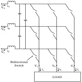
The matrix converter consists of an array of controlled bidirectional switches; in fact with matrix converter is possible to
of three by three bidirectional switches is more interest in industry due to it connects a three phase source to a three phase load
as shown in Fig. 1.
VC VB VA
iC iB iA
ia ib ic
LOAD
Va Vb Vc
[image:3.612.168.433.130.394.2]Bidirectional Switch
Fig. 1. The basic structure of a three phase SiC matrix converter
However, due to lack of energy storage element, voltage transfer ratio of matrix converter is limited to 0.866 and this is a
main disadvantage of matrix converter. Also due to high number of power electronic switches, the switching loss of matrix
converter is higher than other AC-AC power converters.
The EMI filter capacitor of matrix converter which is put in the input of matrix converter requires being a small value for
the application of matrix converter with high input frequency (for example from 360 to 800 Hz) in contrast to standard 50/60
Hz mains application in order to keep the reactive power low and to satisfy the power factor requirement. However, it is needed
a large input capacitance to keep input voltage ripple and harmonic distortion low especially for such application with high
peak output power. Thus this is not applicable because of reactive power limitation. The main solution for this problem is to
raise frequency of switching but it depends on performance, efficiency, volume and weight requirements.
III. THE SIC POWER ELECTRONIC DEVICES
Nowadays SiC power electronic device is known as a high voltage and high switching frequency device in contrast with Si
voltage drop, high switching speed and low thermal resistance [11]. Thus the conduction and switching losses of SiC power
devices could be decreased and the operating temperature could be increased in compare by Si power devices. Therefore, based
on the SiC power devices, achieving highly compact converter systems with lower conduction and switching losses and high
voltage is possible.
Moreover, due to high thermal conductivity and wide band gap energy of SiC, operation in high temperature is allowed to
SiC devices which make them more preferred for harsh environment applications.
Recently, two classes of SiC power electronic devices are commercially available, namely Schottky diodes and transistors.
SiC Schottky diodes are available from several manufacturers, including Infineon, Cree, IXYS, Microsemi, and
STMicroelectronics, etc. The high voltage ratings to 1200 V and the near zero reverse recovery time of these devices, make
them excellent choices for many other hard switching applications. Also SiC controllable switching devices in a variety of
voltage and current levels are available as engineering samples such as JFETs from SemiSouth, MOSFETs from Cree, and
BJTs from TranSiC.
A. Normally-off SiC JFET
One of the most successful and promising device to replace Si-MOSFET and IGBT is the normally-off SiC JFET. The SiC
JFET is the controlled turn on-off SiC device which is close to commercialization and is available as restricted samples. The
SiC JFET is a majority carrier device and its active device structure presents only with P-N junctions. It has been stated that its
surge current capability is better than Si power MOSFET, also its on resistance is lower than 10 mΩcm2 and it has very high
switching speed due to small intrinsic capacitances, thus it is suitable for high switching frequency high power density
application [11].
B. SiC MOSFET
Recently, SiC MOSFETs have become available and some of its advantages have demonstrated. Because the higher doping
and current densities of SiC material, the SiC MOSFETs have smaller area and capacitance, therefore they are more efficient
than Si MOSFETs. The fall time of SiC MOSFET current is smaller, hence switching losses and on state resistance of it is
lower than Si MOSFET [12].
The Cree has introduced a 1200 V SiC MOSFET with low on-state resistance Rds(on) of 160 mΩ, thus removing the upper
voltage limit of silicon MOSFETs [13]. It should be noted that high voltage (>1000 V) Si MOSFETs can be manufactured, but
C. SiC BJT
Many years ago, Si BJT was replaced by Si power MOSFETs and IGBTs due to its low current gain and small safe operating
area which was caused by the unique second breakdown problem. Indeed, there is almost no significant Si BJT research activity
in the past 20 years, but the emergence of SiC as new material for power semiconductor devices has led to consider power
BJTs as a possible candidate for high power and high voltage application. This is due to some advantages of SiC BJTs in
compare with other different SiC power devices which are normally-off device, very low specific on resistance, positive
coefficient of the on resistance, fast switching speed, free from any gate oxide [14]. The 1200V SiC BJTs which have been
developed by TranSiC have overcome the problem of the second breakdown found in Si BJTs and also have better performance
in terms of conduction and switching losses in compare with 1200V Si IGBTs.
Furthermore, one of the vital parameters of the BJT is the common emitter current gain which is defined as the ratio between
the base current and the collector current. It has been reported that the recently fabricated SiC BJTs have a high value for the
common emitter current gain [14]. This means that to obtain the same collector current, the SiC BJT will require a smaller base
current, therefore minimizing base drive loss.
IV. EXPERIMENTAL ARRANGMENT
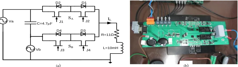
To investigate the switching behavior of SiC devices and measure the power losses of them, three different 2-phase to
1-phase matrix converter with same power layout and PCB trace are implemented. A circuit schematic of 2-1-phase to 1-1-phase
matrix converter is shown in Fig. 2(a). They are populated by four Normally-off SiC JFETs, SiC MOSFETs and SiC BJTs
respectively and four SiC Schottky Diodes which are listed in TABLE I. A prototype of experimental rig of 2-phase to 1-phase
SiC MOSFET matrix converter is shown in Fig. 2(b).
R=11Ω
L=10mH
C=4.7µF
Va
D2 D1
SA
SB
J1 J2
D4 D3
J3 J4
IL
Vb
[image:5.612.60.559.527.669.2]
Fig. 2. 2-phase to 1-phase matrix converter. (a) Schematic of circuit. (b) A prototype of SiC MOSFET matrix converter
To control the switch sequencing using a four step commutation strategy an FPGA is employed. The switching frequency of
converter can be changed and fixed duty cycle switching is used to give equal input and output frequencies. The supply is
variable from 0-230Vrms, 50Hz in each phase and the output current is controlled by adjusting the load resistance. There is a
simple capacitive filter which is constructed from ultra-low inductance metalized polypropylene capacitor at the input side
which connected directly to the power plants.
TABLE I
DIFFERENT POWER SWITCHING DEVICES WHICH ARE USED IN EVALUATION OF THE MATRIX CONVERTER
Switch Model Manufacturer Voltage (V) Current (A) On resistance at TC=25ºC (Ω)
Si IGBT+ diode SK20GB123 Semikron 1200 23 0.086
SiC JFET SJEP120R063 Semisouth 1200 30 0.063
SiC MOSFET CMF10120D CREE 1200 24 0.160
SiC BJT BT1215AC Transic 1200 24 0.075
SiC Diode C4D20120D CREE 1200 32 0.054
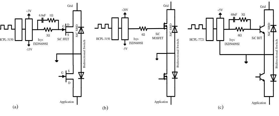
The need to develop suitable gate or base drive in pursue of full utilization of the SiC JFET, MOSFET and BJT high speed
capabilities has hence become apparent, where the major obstacle faced has been the different requests of SiC components. To
solve this problem, several researches have been done to consider special attention which is required [15-19]. In the following
section, different requests for driving SiC power devices and gate or base drives which have been developed and used for
implementation of SiC matrix converter are presented. The gate drive for each device has a similar configuration for the
different SiC devices, but the best performance in terms of switching time has been achieved for each SiC switch. The
configuration of the drive circuit for SiC JFET and BJT is the same but the driving voltage and components are different due
to the requirements of device. An Ixys IXDN609SI as a high speed gate driver with low voltage rise and fall times has been
used in all designed drive circuits to have similar conditions in all tests.
A. Normally-off SiC JFET Gate Drive
Normally-off SiC JFET makes special demands on the gate driver circuit compared to other unipolar SiC or Si devices. To
fully exploit the potential of normally-off SiC JFETs, conventional gate driver circuits for unipolar switches need to be adapted
for use with these switches. As it has been stated in [20], during on-state the gate-source voltage must not exceed 3 V, while a
current of around 150 mA (depending on the desired on-resistance) must be fed into the gate, during switching operation the
transient gate voltage should be around ±15 V and the low threshold voltage of less than 0.7 V requires a high noise immunity
In the existing two stage gate drive [21], one stage supplies a short pulse with a high voltage for turn-on and a second stage
delivers the DC gate current for the on-state. Although the performance of this kind of gate drive is suitable, it still features
high circuit complexity, a high part count, and a large printed circuit board footprint.
A gate drive circuit is developed in order to overcome the current limitations while still having a low circuit complexity. In
the developed gate drive which is shown in Fig. 3(a) is based on AC coupling circuit. It is consist of a gate resistor and a speed
up capacitor. The gate resistor is used to set the DC operating point in the on state by dropping the potential difference between
the high level output of the gate drive IC and the required gate source voltage of the SiC JFET at a specified gate current. The
speed up capacitor is used to rapidly deliver or remove the dynamic gate charge for a fast turn on and off. When the input
capacitance of SiC JFET is fully charged steady state conditions will be regulated by the gate resistor. An additional low
resistance is included in series with the speed up capacitor to dampen any observed gate ringing. The proposed gate drive circuit
is designed to control a 1.2 kV- 30 A normally-off SiC JFET (SJEP120R063) from the Semisouth. The other components of
the drive circuit are an Ixys IXDN609SI which provide 18V output swing and up to 9A of current and an opto-isolator, the
Avago HCPL-3150 which has high common mode transient immunity (15kV/μsec) and can operate from 15 to 30V.
HCPL-3150 SiC JFET S
iC S B D +3V -15V B id ir e c ti o n a l S w it c h Grid Application 6.8nF S D G S G D 1Ω 3Ω Ixys IXDN609SI HCPL-3150 SiC MOSFET S iC S B D +20V -5V B id ir e c ti o n a l S w it c h Grid Application 4Ω Ixys IXDN609SI
HCPL-7721 SiC BJT
[image:7.612.63.540.398.596.2]S iC S B D +5V B id ir e c ti o n a l S w it c h Grid Application 68nF 3Ω 6Ω Ixys IXDN609SI
Fig. 3. A schematic diagram of drive circuits for SiC devices. (a) Gate drive of SiC JFET.(b) Gate drive of SiC MOSFET.(c) Base drive of SiC BJT
B. SiC MOSFET Gate Drive
The proposed gate drive circuit for SiC MOSFET is indicated in Fig. 3(b) and consists of a current limiting resistor. It is
designed to control a 1.2 kV- 24 A SiC MOSFET (CMF10120D) from CREE. The other components which are used in drive
circuit are an Ixys IXDN609SI which provides 25V output swing and up to 9A of current and an optoisolator, the Avago HCPL-7721, which has high common mode transient immunity (15kV/μsec) and can operate from 15 to 30V.
C. SiC BJT Base Drive
It has been stated that the base drive requirements of SiC BJTs are totally different from Si BJTs [22]. This is due to the SiC
BJT does not rely on high injection and there is no problems with storage times at turn off. Also if the reverse base current
during the turn off is too high, the SiC BJT does not have problem with trapped charge [23]. Thus, these features make it clear
that the design criteria of SiC BJT are different from Si BJT.
As it is mentioned, the main argument against the SiC BJT is the base current when it is in the on state due to it must be
produced by the base drive circuit and the amount of required base current is not negligible. Typical values of the common
emitter gain are of the order 60, which mean that a 30 A SiC BJT would need a base current of the order of 0.5A[23].
A well-known base drive circuit that improves the switching transients is an AC coupling circuit which is illustrated in
Fig.3(c). It is consists of a base resistor and a speed up capacitor in parallel with resistor. The capacitor is charged up to a
voltage level equal to the voltage difference between VCC and VBE(SAT) during the turn on transition of SiC BJT and so creating a low impedance path for the base current. In addition, the capacitor provides a negative voltage which applied across the base
emitter terminals during the turn off transition of the SiC BJT. This causes improvement in the turn off transient.
The proposed base drive circuit is designed to control a 1.2 kV- 24 A SiC BJT (BT1215AC) from TranSiC. The main
component of the circuit is an Ixys IXDN609SI which can provide 5Voutput swing and up to 9A of current. The optoisolator,
the Avago HCPL-7721, has high common mode transient immunity (10kV/μsec) and can operate from 4.5 to 5.5V.
V. SWITCHING PERFORMANCE EVALUATION
To investigate experimentally performance of different SiC power devices in matrix converter, the current and voltage
switching waveforms for all SiC power devices in each of the three SiC matrix converters were measured under identical
operating conditions. Then, the input and output power of three matrix converters in different temperatures and switching
frequencies are measured in order to extract the power loss from them.
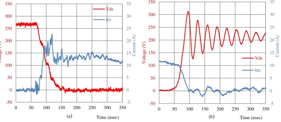
A. Turn on waveform
With implemented SiC matrix converters, turn on switching performance of SiC power devices has been tested in various
JFET in matrix converter when the case temperature of device is 25ºC is shown in Fig.4(a). It is obvious that the switching turn
[image:9.612.64.541.126.318.2]on time is slightly less than 50 ns.
Fig. 4. Switching waveforms of the normally-off SiC JFET at VSW=270 V and ISW=15 A when TC=25ºC. (a) Turn on switching waveform. (b) Turn off
switching waveform
Fig. 5. Switching waveforms of the SiC MOSFET at VSW=270 V and ISW=13 A when TC=25ºC. (a) Turn on switching waveform. (b) Turn off switching
waveform -5 0 5 10 15 20 25 30 -50 0 50 100 150 200 250 300
0 50 100 150 200 250 300 350
C u rr en t (A ) V o lt ag e (V ) Time (nsec) Vds (V) Ids (A) -5 0 5 10 15 20 25 30 35 -50 0 50 100 150 200 250 300 350
0 50 100 150 200 250 300 350
C u rr en t (A ) V o lt ag e (V ) Time (nsec) Vds Ids -5 0 5 10 15 20 25 30 35 -50 0 50 100 150 200 250 300 350
0 50 100 150 200 250 300 350
C u rr en t (A ) V o lt ag e (V ) Time (nsec) Vds Ids -5 0 5 10 15 20 25 30 35 -50 0 50 100 150 200 250 300 350
0 50 100 150 200 250 300 350
C u rr en t (A ) V o lt ag e (V ) Time (nsec) Vds Ids
(a) (b)
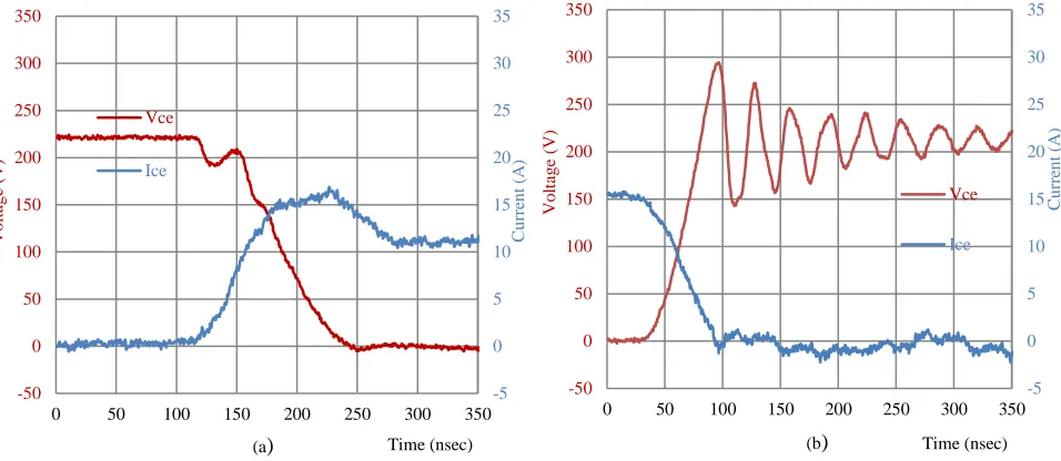
[image:9.612.62.543.374.584.2]Fig. 6. Switching waveforms of the SiC BJT at VSW=230 V and ISW=15 A when TC=25ºC. (a) Turn on switching waveform. (b) Turn off switching
waveform
In addition, Fig.5(a) shows the waveforms of drain-source voltage and drain current for turning on the SiC MOSFET in matrix
converter when the case temperature of device is 25ºC. It is clear that the switching turn on time is slightly more than 80 ns.
Moreover, the waveforms of collector-emitter voltage and collector current for turning on the SiC BJT in matrix converter
when case temperature of devices is 25ºC is illustrated in Fig.6(a). Based on the illustrated waveform for SiC BJT, it can be
stated that turning on time of SiC BJT is about 140 ns which is more than two other SiC switches.
B. Turn off waveform
The waveforms of drain to source voltage and drain current during turning off process of the normally-off SiC JFET in
matrix converter when case temperature of devices is about 25 ºC is indicated in Fig.4(b). It is clear that the switching turn off
time when the voltage across the switch and load current are 260 V and 15 A respectively is slightly more than 65 ns.
Furthermore, the waveforms in Fig.5(b) shows drain to source voltage and drain current during turning off process of the SiC
MOSFET in matrix converter. It is obvious that the turning off time of it when the voltage across the device and load current
are 220 V and 13 A respectively is slightly more than 85 ns. Moreover, the turning off time of SiC BJT in matrix converter
when the temperature of devices case, voltage across collector-emitter of device and load current are 25ºC, 210V and 15 A
respectively is about 55 ns, based on presented waveform in Fig.6(b). There is overshoot and distinct oscillation in waveform
of turning off voltage of SiC devices which is due to parasitic inductance of PCB circuit. -5 0 5 10 15 20 25 30 35 -50 0 50 100 150 200 250 300 350
0 50 100 150 200 250 300 350
C u rr en t (A ) V o lt ag e (V ) Time (nsec) Vce Ice -5 0 5 10 15 20 25 30 35 -50 0 50 100 150 200 250 300 350
0 50 100 150 200 250 300 350
C u rr en t (A ) V o lt ag e (V ) Time (nsec) Vce Ice
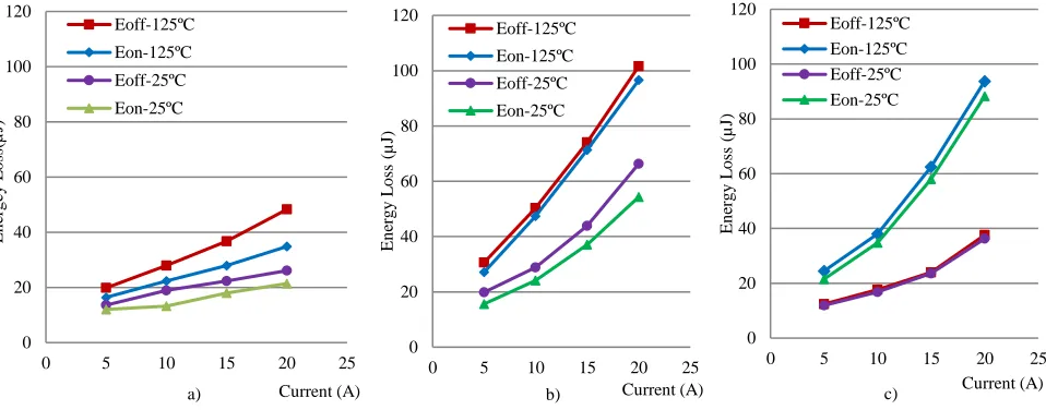
C. Switching Energy Losses
In order to estimate the switching loss of a three phase matrix converter in future section, it is needed to know the value of
the energy loss during turning on and off process of each SiC devices. Therefore, the switching energy losses of SiC power
devices were calculated in different temperatures and currents. Indeed, the switching characterization has been done for current
up to 20 A when the input voltage is 250 V and the case temperature is 25 and 125 ºC. The switching energy loss was calculated
by the integration of the instantaneous power waveform (drain-source (collector-emitter) voltage waveform multiplied by drain
(collector) current waveform). In addition, Fig. 7 shows the switching energy losses of Normally-off SiC JFET, SiC MOSFET
and SiC BJT in different temperatures and currents when they are employed in matrix converter. It is seen that the SiC MOSFET
has a larger total switching energy loss than Normally-off SiC JFET and SiC BJT. Also by increasing the temperature, the
switching energy loss of SiC MOSFET has been increased significantly in compare with Normally-off SiC JFET and SiC BJT.
Fig. 7. Switching energy losses of SiC power devices in different load currents and temperatures at VSW=250 V. (a) Normally-off SiC JFET.(b) SiC
MOSFET.(c) SiC BJT
D. Performance Evaluation of SiC Matrix Converter
The switching waveforms which indicted in Fig. 4, 5 and 6 are suitable for comparing switching phenomena in terms of
voltage overshoot; turn on and off times of switching and switching energy losses. The power loss can be determined by
measuring the input and output power of matrix converter. The instantaneous input and output powers can be determined by
measuring input and output currents and voltages. This was done using differential voltage probe and Hall Effect current probe.
Then the input and output powers of matrix converter were determined by multiplying the current and voltage of them. The
instantaneous powers were integrated over several cycles of the input and output waveforms at the sampling frequency of
0 20 40 60 80 100 120
0 5 10 15 20 25
En er g ey L o ss( µ J) Current (A) Eoff-125ºC Eon-125ºC Eoff-25ºC Eon-25ºC a) 0 20 40 60 80 100 120
0 5 10 15 20 25
En er g y L o ss (µ J) Current (A) Eoff-125ºC Eon-125ºC Eoff-25ºC Eon-25ºC b) 0 20 40 60 80 100 120
0 5 10 15 20 25
[image:11.612.63.542.313.501.2]500MHz to ensure good accuracy in calculating. The advantage of using this method is that any random errors for instance
due to noise, will tend to cancel.
In order to compare the performance of the three SiC power devices in terms of the overall efficiency and the power loss,
the input and output powers are measured over a wide range of switching frequency and different operating temperatures.
Different heatsinks have been employed to change the case temperature of switches.
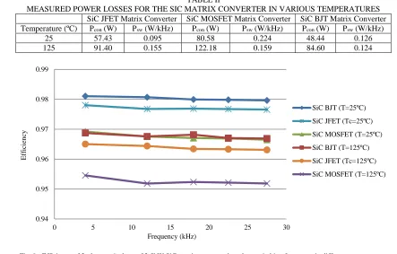
Figure 8 shows the measured power losses of matrix converter when different SiC devices have been employed in it based
on the switching frequency in different operating temperatures for 2.5 kW converter. It is obvious that the power loss of SiC
BJT matrix converter is less than the SiC JFET and MOSFET matrix converters. It is clear that by increasing the switching
[image:12.612.61.544.293.462.2]frequency, there is no significant increasing in the power losses of SiC matrix converters.
Fig. 8. Measured power losses of 2.5 kW SiC matrix converter in different switching frequencies and temperatures. (a) SiC JFET.(b) SiC MOSFET.(c) SiC
BJT
Furthermore, the switching loss per unit switching frequency (Psw) can be calculated from the gradient of power loss curve in Fig. 8. Also the conduction loss (Pcon) of matrix converter can be determined from the intersection of power loss curve with zero switching frequency in Fig. 8. The values listed in TABLE II are taken from results presented in Fig.8.
Due to same SiC diode has been used with three different SiC devices in matrix converter, so the difference in the conduction
losses of SiC matrix converters is because of different kind of SiC power devices. In the other hand, due to conduction loss of
SiC JFET, MOSFET and BJT only depends to the on resistance of devices and load current, thus, it can be stated that the on
resistance of SiC MOSFET is more than SiC JEFT and BJT. It is interesting to note that the conduction loss of SiC MOSFET
matrix converter has been increased more than conduction loss of two other SiC matrix converters by increasing temperature,
so it can be concluded that the on resistance of SiC MOSFET is increased more by increasing temperature
40 50 60 70 80 90 100 110 120 130 140
0 10 20 30
P o w er L o ss (W ) Frequency(kHz) Tc=125ºC Tc=25ºC (a) 40 50 60 70 80 90 100 110 120 130 140
0 10 20 30
P o w er L o ss (W ) Frequency (kHz) Tc=125ºC Tc=25ºC 40 50 60 70 80 90 100 110 120 130 140
0 10 20 30
P o w er L o ss (W ) Frequency (kHz) Tc=125ºC Tc=25ºC
Fig. 9.: Efficiency of 2-phase to 1-phase of 2.5kW SiC matrix converter based on switching frequency in different temperatures
Fig. 10.: Efficiency of 2-phase to 1-phase SiC matrix converter based on output power in different switching frequencies at TC=25ºC
In addition based on the measured input and output power of matrix converter for various switching frequencies and
temperatures, the efficiency has been determined which has been illustrated in Fig.9. It is clear that the efficiency of SiC matrix
converters are slightly varied by changing switching frequency and temperature. Also, the efficiency of three SiC matrix
converters is more than 95% in high frequency and high temperature. Furthermore, Fig.10 illustrates the efficiency of the three
0.94 0.95 0.96 0.97 0.98 0.99
0 5 10 15 20 25 30
Ef
fi
ci
en
cy
Frequency (kHz)
SiC BJT (T=25ºC)
SiC JFET (Tc=25ºC)
SiC MOSFET (T=25ºC)
SiC BJT (T=125ºC)
SiC JFET (Tc=125ºC)
SiC MOSFET (T=125ºC)
0.96 0.965 0.97 0.975 0.98 0.985 0.99 0.995
0 500 1000 1500 2000 2500 3000
Ef
fi
ci
en
cy
Power (W)
SIC BJT Fsw=4 kHz
SiC BJT Fsw=27.5 kHz
SiC JFET Fsw=4 kHz
SiC JFET Fsw=27.5 kHz
SiC MOSFET Fsw=4 kHz
SiC MOSFET Fsw=27.5 kHz TABLE II
MEASURED POWER LOSSES FOR THE SIC MATRIX CONVERTER IN VARIOUS TEMPERATURES SiC JFET Matrix Converter SiC MOSFET Matrix Converter SiC BJT Matrix Converter Temperature (ºC) Pcon (W) Psw (W/kHz) Pcon (W) Psw (W/kHz) Pcon (W) Psw (W/kHz)
25 57.43 0.095 80.58 0.224 48.44 0.126
SiC matrix converters based on the output power in different switching frequencies. It is obvious that the efficiency variation
of SiC JFET and BJT matrix converters is less than SiC MOSFET matrix converter.
VI. POWER LOSS EVALUATION IN THREE PHASE MATRIX CONVERTER
One of the basic steps for evaluation of the reliability of matrix converter is power loss analysis. Due to converting AC utility
voltages into variable voltage outputs in matrix converter by nine bidirectional switches, the drain-source or collector-emitter
voltage of JFET and MOSFET or BJT and IGBT switches are not constant at each switching instant. Also due to rotation of
voltage angle of utility grid, the current distributions in each switch changes. For these reasons, evaluation of switching losses
in matrix converter requires conceptual understanding of switching rules and physical characteristics of switches and diodes.
Calculation of conduction loss and switching loss for matrix converter has been conducted in [24-26].
This part of paper presents an analytical method for evaluating power losses of three phase matrix converter with Si and SiC
power devices and then comparison of them. Power device losses of matrix converter consist of drive, conduction and switching
losses of diodes and switch devices such as Si IGBT and SiC JFET, MOSFET or BJT. In the calculation of conduction loss in
next section, the on resistance and on state voltage of devices have been extracted from the device datasheet, while in calculation
of matrix converter switching losses, the measured switching energies from 2-phase matrix converters in previous section have
been used.
A. Drive Losses
Power consumption in the drive circuit is required to consider in determining the efficiency of whole converter. The drive
losses in various power switching devices is different and it depends on the characteristics of switch and drive circuit.
For the normally-off SiC JFET, three contributions of the power consumption must be considered in calculation the drive
losses based on the used gate drive circuit in previous section. The first one is associated with charging of the gate capacitance
during each turn on transient. The second one is due to on state resistance of the gate drive and the last one is associated with
charging of speed up capacitor in the gate drive. Therefore the total drive loss for the normally-off SiC JFET can be presented
as:
𝑃𝑑𝑟𝑖𝑣𝑒−𝐽𝐹𝐸𝑇 = 𝑉𝑔𝑠𝑄𝑔𝑓𝑠+ 𝐼𝑔𝑟𝑚𝑠2 𝑅𝑔+ 𝐶𝑠𝑓𝑠(𝑉𝑐𝑐− 𝑉𝑔𝑠)2 (1)
In the above equation, 𝑉𝑔𝑠is the forward voltage bias, 𝑄𝑔is the gate charge of JFET, 𝑓𝑠is the switching frequency, 𝐼𝑔𝑟𝑚𝑠is the
In addition, the drive loss of SiC MOSFET and Si IGBT only consists of the charging of the gate capacitance during each
turn on transient. Therefore it can be stated as:
𝑃𝑑𝑟𝑖𝑣𝑒−𝑀𝑂𝑆𝐹𝐸𝑇 𝑜𝑟 𝐼𝐺𝐵𝑇 = 𝑉𝑔𝑠𝑄𝑔𝑓𝑠 (2)
In the above equation, 𝑉𝑔𝑠is the forward voltage bias, 𝑄𝑔is the gate charge of MOSFET or IGBT and 𝑓𝑠 is the switching
frequency.
Furthermore, for determining the base drive losses of SiC BJT, it is needed to consider one more contribution of power
consumption in compare with normally-off SiC JFET which is due to voltage drop across the base emitter of BJT in on state
duration. Therefore, the total base drive losses for the SiC BJT based on the used base drive circuit in this work can be expressed
as:
𝑃𝑑𝑟𝑖𝑣𝑒−𝐵𝐽𝑇= 𝐼𝑏𝑎𝑣𝑉𝑏𝑒(𝑠𝑎𝑡)+ 𝑉𝑏𝑒(𝑠𝑎𝑡)𝑄𝑏𝑓𝑠+ 𝐼𝑏𝑟𝑚𝑠2 𝑅𝑏+ 𝐶𝑠𝑓𝑠(𝑉𝑐𝑐− 𝑉𝑏𝑒(𝑠𝑎𝑡))2 (3)
In the above equation, Ibav is the average base current, 𝑉𝑏𝑒(𝑠𝑎𝑡)is the voltage drop across based emitter of BJT, 𝑄𝑏is the base charge of BJT, 𝑓𝑠is the switching frequency, 𝐼𝑏𝑟𝑚𝑠is the rms value of the base current, 𝑅𝑏is the base resistor, 𝐶𝑠 is the speed up
capacitor and 𝑉𝑐𝑐is the supply voltage in turn on time.
Therefore, by considering a typical double sided space vector modulation for matrix converter, the total driving loss of the
three phase matrix converter can be calculated by:
𝑃𝑑𝑟𝑖𝑣𝑒 = 12𝑃𝑑𝑟𝑖𝑣𝑒−𝐽𝐹𝐸𝑇 𝑜𝑟 𝑀𝑂𝑆𝐹𝐸𝑇 𝑜𝑟 𝐵𝐽𝑇 𝑜𝑟 𝐼𝐺𝐵𝑇 (4)
B. Conduction Losses
Conduction losses of switching devices in matrix converter have been covered in [25, 27]. In fact, the output current flow
through one switching devices such as JFET or IGBT and one diode at any instant, thus based on the balanced three phase
output currents some equations have been derived to determine conduction losses with depend on the model of switch [27]. By
assuming a sinusoidal output current of rms magnitude Io, the average conduction losses for three phase matrix converter for
different switch devices is given by:
𝑃𝑐𝑜𝑛 =6√2𝜋 𝑉𝑐𝑒𝐼𝑜+ 3𝑟𝑐𝑒𝐼𝑜2 (5) (for Si IGBT)
𝑃𝑐𝑜𝑛= 3𝑟𝑑𝑠 𝐼𝑜2 (6) (for SiC JFET, MOSFET and BJT)
𝑃𝑐𝑜𝑛= 3𝑟𝑐𝑒 𝐼𝑜2 (7) (for SiC BJT)
In the above equation, Vce is the on-state collector-emitter voltage of IGBT switch and rce is on state resistance of IGBT or BJT switch. Also rds is on state resistance of JFET or MOSFET and Vf and rd are the diode forward voltage drop at zero current and the on state resistance of diode respectively.
It is obvious that the conduction loss is only calculated by the rms value of the output current and the operation conditions
such as modulation index or switching frequency do not have any effect.
C. Switching Losses
The turn on and turn off energy losses for a power electronic switch can be assumed to vary linearly with the change in
voltage across the power electronic switch during the switching transient [25]. Also, it is reasonable to assume that the turn on
and turn off energy losses varies linearly with the blocking voltage and the conducting current of power electronic switch at
the instant of switching event [25]. Hence, the rate of turn on and off of switching energy losses at the reference voltage and
current are computed using the following equations:
𝐸𝑜𝑛=𝑉𝑒𝑜𝑛
𝑅𝐼𝑅 (9)
𝐸𝑜𝑓𝑓= 𝑒𝑜𝑓𝑓
𝑉𝑅𝐼𝑅 (10)
In the above equations, eon and eoff are the turn on and turn off energy losses of switching device respectively. VR is the reference voltage in the drain-source or collector-emitter of JFET and MOSFET or BJT and IGBT respectively. IR is the reference current in the drain or collector of JFET and MOSFET or BJT and IGBT respectively.
Similarly the rate of diode reverse recovery or turn off switching energy loss is determined using:
𝐸𝑟𝑒𝑐 =𝑉𝑒𝑟𝑒𝑐
𝑅𝐼𝑅 (11)
In the above equation, erec is the diode recovery or turn off energy loss. VR is the reference voltage across the diode and IR is the reference current of the diode.
In the other hand, for calculating switching losses, it is important to know the mechanisms of commutation due to its effect
on switching. Commutation in matrix converter is not as straightforward as in conventional inverters since there are no natural
free-wheeling paths. In a matrix converter, the commutation between two bidirectional switches is dependent on both the
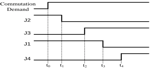
Fig. 11. Timing diagram indicting typical device sequencing when using a four step commutation strategy
Different commutation schemes are possible depending on the direction of the load current, and the relative potentials of
input voltage. The device gate timings for a four step commutation strategy when commutating from SA to SB with the load
current, IL in the direction indicated in Fig.2 (a) is shown in Fig. 11. If input voltage is positive, commutation will occur at t3
resulting in a hard turn-off in SA (J1) and a soft turn-on in SB (J3). Conversely, if input voltage is negative, commutation takes
place at t2 resulting in a hard turn-on in SB (J3) and a soft turn-off in SA (J1). It is worth to note that, there is no switching loss
at all in J2 and J4 for either situation, since neither conduct current when IL is positive. A similar, but different sequence of
events to that above occurs for negative IL. The soft commutations are not completely lossless, but the energy involved is at
least an order of magnitude less than for the hard commutations.
As it has been stated in [24], the observation from the four step commutation scheme can be generalized that there are one
turn on loss transient, and one turn off loss transient for the switches and also one reverse recovery energy loss for diode in
each commutation event. So by considering symmetry of the balance three phase systems at the input and output terminals of
three phase matrix converter, the total switching energy loss of one phase in one switching cycle can be determined by:
𝐸𝑠𝑤= (𝐸𝑜𝑛+ 𝐸𝑜𝑓𝑓+ 𝐸𝑟𝑒𝑐)(|𝑉12| + |𝑉23|)|𝑖𝑜1| (12)
In the above equation, V12 and V23 are phase to phase voltage and io1 is the output current of matrix converter.
By considering that the switching frequency is much higher than the fundamental frequency of input voltage and output
current and also a typical double sided space vector modulation, the total switching loss of the three phase matrix converter can
be calculated by:
𝑃𝑠𝑤=24√3𝜋2 𝑓𝑠(𝐸𝑜𝑛+ 𝐸𝑜𝑓𝑓+ 𝐸𝑟𝑒𝑐)𝑉𝑖𝐼𝑜 (13)
In the above equation, 𝑓𝑠is the switching frequency of matrix converter and also 𝑉𝑖 and 𝑖𝑜 are peak value of input voltage
and output current of matrix converter respectively.
D. Comparison of Power Losses in Matrix Converter with various power electronic switches
Commutation Demand
J2
J3
J1
J4
t4
t3
t2
t1
To determine and evaluate power losses in matrix converter with various power switching devices three phase matrix
converter is considered and four-step commutation strategy is applied. Also, it is considered four kind of matrix converter with
four different switching devices for calculating and comparing the power losses of matrix converter. Four different switch
devices which are used in evaluation of matrix converter are listed in TABLE I. Input rms voltage and frequency of matrix
converter are 230 V and 50 Hz respectively and output rms voltage and frequency of matrix converter are set 150 V and 400
Hz respectively. The value of the resistance and inductance of the load which are supplied by matrix converter are 10 Ω and
1.3 mH respectively.
Based on the mentioned equations for calculating drive, conduction and switching losses, determined conduction losses and
switching energies in previous section and some parameters from the gate or base drive circuit and datasheet of power switching
devices, the drive, conduction and switching losses of matrix converter for various switching devices are determined. Figure
12 shows the comparison of the drive loss, conduction loss and switching loss between Si IGBTs, SiC MOSFETs, SiC JFETs
and SiC BJTs in three phase matrix converter when switching frequency and output power of converter are 80 KHz and 7 KW
respectively. It can be stated that there is a significant decreasing in switching losses of SiC matrix converter due low switching
energy losses of SiC BJT, JFET and MOSFET in compare with Si IGBT. Also there is no on state voltage across drain-source
of SiC JFET or collector-emitter of SiC BJT, so conduction loss in SiC JFET and SiC BJT is lower than Si IGBT. It is worth
to mention that due to high on resistance of SiC MOSFET in compare by other devices, the total conduction loss of SiC
MOSFETs are more than Si IGBTs and other SiC devices in matrix converter, although there is no on state voltage across
drain-source of SiC MOSFET. It is worth to mention that the amount of drive loss of SiC BJT is not significant in compare by
other kind of losses so the total power losses of a SiC BJT matrix converter has not been affected dramatically due to drive loss
Fig. 12. Drive, conduction and switching losses of Si and SiC power devices in a 7 KW three phase matrix converter when switching frequency is 80 kHz at
TC=25ºC.
Fig. 13. Conduction and switching losses of Si diode and SiC schottky diode in a 7 KW three phase Matrix converter when switching frequency is 80 kHz at
TC=25ºC.
In addition, Fig. 13 shows the comparison of the conduction and turn-off losses between Si diodes and SiC Schottky diodes
which are used in three phase matrix converter. The most significant difference between Si diode and SiC Schottky diode is in
turn off loss due to there is no reverse recovery current in SiC schottky diode in compare with Si diode.
0 50 100 150 200 250 300 350 400 450 500
Conduction Loss Turn-on Loss Turn-off Loss Drive Loss
P
o
w
er
L
o
sse
s
(W
)
Si IGBTs
SiC MOSFETs
SiC JFETs
SiC BJTs
0 20 40 60 80 100 120 140 160 180
Conduction Loss Turn-off Loss
P
o
w
er
L
o
ss
es
(W
)
Si Diodes
[image:19.612.201.416.333.515.2]Fig. 14. Calculated efficiency of 7 KW matrix converter for various devices in different switching frequencies at TC=25ºC
The efficiency of the Si and SiC matrix converters for different switching frequencies when the load that supplied by matrix
converter is 7 KW is also studied. The calculation result is shown in Fig. 14. It is obvious that efficiency of a three phase matrix
converter which is built by SiC power devices is not reduced rapidly by increasing the switching frequency in compare with a
Si matrix converter. This calculation also shows that high power SiC matrix converter would approximately have an efficiency
that exceeds 94% in high switching frequency when is built by SiC MOSFET or even it can have 96% when is implemented
by normally-off SiC JFET or SiC BJT.
VII. CONCLUSION
This paper has focused on performance comparison of different Si and SiC devices in the matrix converter topology. The
study was supported by the measurement of the switching characteristics of normally-off SiC JFET, SiC MOSFET and SiC
BJT in bidirectional switch arrangement of 2-phase to 1-phase matrix converter. It has been shown that base on the developed
gate or base drives; it is possible to achieve turn on time less than 55, 80 and 140 ns for SiC JFET, MOSFET and BJT
respectively. Also the measured turn off time was less than 65, 85 and 55 ns for SiC JFET, MOSFET and BJT respectively.
Based on the measured input and output power of SiC matrix converters the performance of them in terms of power loss and
efficiency has been investigated in various switching frequencies, load currents and case temperatures. It has been shown that
the performance of 2-phase to 1-phase SiC matrix converter in terms of efficiency has been decreased very slightly by
increasing switching frequency and temperature case of SiC devices. Among different SiC devices, SiC BJT amd JFET has
0.8 0.82 0.84 0.86 0.88 0.9 0.92 0.94 0.96 0.98 1
0 10 20 30 40 50 60 70 80 90
Ef
fi
ci
en
cy
Frequency (kHz) Si IGBTs-Diodes
SiC MOSFETs-Diodes
SiC JFETs-Diodes
shown higher efficiency in compare with SiC MOSFET in high temperature and switching frequency.
Analytical descriptions for calculating power losses in matrix converter are presented and then power losses of Si and SiC
matrix converter are determined in various frequencies. It has been shown that high power SiC matrix converter would
approximately have an efficiency that exceeds 96%. It can be concluded that, the power electronic switches realized with SiC
are respectable devices which will ensure the loss reduction and the improvement of power density in future.
REFERENCES
[1] T. R. McNutt, A. R. Hefner, H. A. Mantooth, D. Berning, and R. Sei-Hyung, "Silicon Carbide Power MOSFET Model and Parameter Extraction Sequence," Power Electronics, IEEE Transactions on, vol. 22, pp. 353-363, 2007.
[2] T. Funaki, J. C. Balda, J. Junghans, A. S. Kashyap, H. A. Mantooth, F. Barlow, T. Kimoto, and T. Hikihara, "Power Conversion With SiC Devices at Extremely High Ambient Temperatures," Power Electronics, IEEE Transactions on, vol. 22, pp. 1321-1329, 2007.
[3] R. A. Wood and T. E. Salem, "Evaluation of a 1200-V, 800-A All-SiC Dual Module," Power Electronics, IEEE Transactions on, vol. 26, pp. 2504-2511, 2011.
[4] J. Biela, M. Schweizer, S. Waffler, and J. W. Kolar, "SiC versus Si-Evaluation of Potentials for Performance Improvement of Inverter and DC-DC Converter Systems by SiC Power Semiconductors," Industrial Electronics, IEEE Transactions on, vol. 58, pp. 2872-2882, 2011.
[5] C. J. Cass, R. Burgos, F. Wang, and D. Boroyevich, "Improved charge control with adjustable input power factor and optimized switching pattern for a 150 kHz three-phase buck rectifier," in Applied Power Electronics Conference and Exposition, 2008. APEC 2008. Twenty-Third Annual IEEE, 2008, pp. 1200-1206.
[6] L. Rixin, F. Wang, N. Puqi, Z. Di, J. Dong, R. Burgos, D. Boroyevich, K. J. Karimi, and V. D. Immanuel, "Development of a 10 kW high power density three-phase ac-dc-ac converter using SiC devices," in Power Electronics and Applications, 2009. EPE '09. 13th European Conference on, 2009, pp. 1-12.
[7] T. Friedli, S. D. Round, and J. W. Kolar, "A 100 kHz SiC Sparse Matrix Converter," in Power Electronics Specialists Conference, 2007. PESC 2007. IEEE, 2007, pp. 2148-2154.
[8] S. Safari, A. Castellazzi, and P. Wheeler, "Evaluation of normally-off SiC JFET for a high power density matrix converter," in Power Electronics and Motion Control Conference (EPE/PEMC), 2012 15th International, 2012, pp. DS1a.9-1-DS1a.9-7.
[9] S. Safari, A. Castellazzi, and P. Wheeler, "Evaluation of SiC power devices for a high power density matrix converter," in Energy Conversion Congress and Exposition (ECCE), 2012 IEEE, 2012, pp. 3934-3941.
[10] P. W. Wheeler, J. Rodriguez, J. C. Clare, L. Empringham, and A. Weinstein, "Matrix converters: a technology review,"
Industrial Electronics, IEEE Transactions on, vol. 49, pp. 276-288, 2002.
[11] B. Wrzecionko, S. Kach, D. Bortis, J. Biela, and J. W. Kolar, "Novel AC coupled gate driver for ultra fast switching of normally-off SiC JFETs," in IECON 2010 - 36th Annual Conference on IEEE Industrial Electronics Society, 2010, pp. 605-612.
[12] X. Xu, A. Q. Huang, Y. Gao, A. Agarwal, S. Krishnaswami, S.-H. Ryu, and X. Huang, "Performance Evaluation of SiC MOSFET/BJT/Schottky Diode in A 1MHz Single Phase PFC," in Applied Power Electronics Conference, APEC 2007 - Twenty Second Annual IEEE, 2007, pp. 1268-1272.
[13] R. J. Callanan, A. Agarwal, A. Burk, M. Das, B. Hull, F. Husna, A. Powell, J. Richmond, R. Sei-Hyung, and Z. Qingchun, "Recent progress in SiC DMOSFETs and JBS diodes at Cree," in Industrial Electronics, 2008. IECON 2008. 34th Annual Conference of IEEE, 2008, pp. 2885-2890.
2010.
[15] S. Waffler, S. D. Round, and J. W. Kolar, "High temperature (>>200°C) isolated gate drive topologies for Silicon Carbide (SiC) JFET," in Industrial Electronics, 2008. IECON 2008. 34th Annual Conference of IEEE, 2008, pp. 2867-2872. [16] R. Burgos, C. Zheng, D. Boroyevich, and F. Wang, "Design considerations of a fast 0Ω; gate-drive circuit for 1.2 kV SiC JFET devices in phase-leg configuration," in Energy Conversion Congress and Exposition, 2009. ECCE 2009. IEEE, 2009, pp. 2293-2300.
[17] D. Domes, R. Werner, W. Hofmann, K. Domes, and S. Kraub, "A New, Universal and Fast Switching Gate-Drive-Concept for SiC-JFETs based on Current Source Principle," in Power Electronics Specialists Conference, 2006. PESC '06. 37th IEEE, 2006, pp. 1-6.
[18] K. Mino, S. Herold, and J. W. Kolar, "A gate drive circuit for silicon carbide JFET," in Industrial Electronics Society, 2003. IECON '03. The 29th Annual Conference of the IEEE, 2003, pp. 1162-1166 Vol.2.
[19] I. Abuishmais, S. Basu, and T. M. Undeland, "On understanding and driving SiC power JFETs," in Applied Power Electronics Conference and Exposition (APEC), 2011 Twenty-Sixth Annual IEEE, 2011, pp. 1071-1075.
[20] B. Wrzecionko, D. Bortis, J. Biela, and J. Kolar, "Novel AC Coupled Gate Driver for Ultra Fast Switching of Normally-Off SiC JFETs," Power Electronics, IEEE Transactions on, vol. PP, pp. 1-1, 2011.
[21] I. SemiSouth Laboratories, "Two-Stage Opto Coupled Gate DriverDemo Board, ," SemiSouth Laboratories, Inc., 201Research Boulevard, Starkville, MS 39759, USA, Feb, 2010.
[22] J. Rabkowski, D. Peftitsis, H.-P. Nee, and M. Zdanowski, "A simple high-performance low-loss current-source driver for SiC bipolar transistors," in Power Electronics and Motion Control Conference (IPEMC), 2012 7th International, 2012, pp. 222-228.
[23] J. Rabkowski, G. Tolstoy, D. Peftitsis, and H. Nee, "Low-Loss High-Performance Base-Drive Unit for SiC BJTs,"
Power Electronics, IEEE Transactions on, vol. 27, pp. 2633-2643, 2012.
[24] B. Wang and G. Venkataramanan, "Analytical Modeling of Semiconductor Losses in Matrix Converters," in Power Electronics and Motion Control Conference, 2006. IPEMC 2006. CES/IEEE 5th International, 2006, pp. 1-8.
[25] K. Jun-Koo, H. Hara, E. Yamamoto, and E. Watanabe, "Analysis and evaluation of bi-directional power switch losses for matrix converter drive," in Industry Applications Conference, 2002. 37th IAS Annual Meeting. Conference Record of the, 2002, pp. 438-443 vol.1.
[26] F. Schafmeister, S. Herold, and J. W. Kolar, "Evaluation of 1200 V-Si-IGBTs and 1300 V-SiC-JFETs for application in three-phase very sparse matrix AC-AC converter systems," in Applied Power Electronics Conference and Exposition, 2003. APEC '03. Eighteenth Annual IEEE, 2003, pp. 241-255 vol.1.