© 2019, IRJET | Impact Factor value: 7.211 | ISO 9001:2008 Certified Journal
| Page 5981
Design and Implementation of PWM Rectifier with Power Factor
Control
R. Santhoshkumar
1, Dr. P. Maruthupandi
21
ME-Power Electronics and Drives, Department of Electrical and Electronics Engineering, Government College of
Technology, Coimbatore, Tamil nadu, India
2
Assistant Professor, Department of Electrical and Electronics Engineering, Government College of Technology,
Coimbatore, Tamil nadu, India
---***---Abstract - This paper analyzes the principle of the PWMrectifier, with a variable unity power factor control method of the PWM rectifier. Controller used closed-loop PI control, which inner uses single-phase input current control method controlled by power factor and controls the output DC voltage of rectifier. Voltage phase detection methods proposed could eliminate the affection of the voltage harmonics on phase detection accuracy. The results of the simulation and experiment verify the feasibleness and effectiveness of the tactic.
Keywords — PWM, rectifier, power factor control, filter,
current control, closed loop control.
I.INTRODUCTION
Since the rectifier consisted of the thyristor is easy to control and reliable, it is widely used in the industry. However, the input current control of this rectifier contains many harmonics, which has become the main source of the grid. In addition, this rectifier also about has a low power factor. PWM rectifier not produced to harmonics on the grid, the input power factor has been controlled and the output DC voltage can be adjusted, is
A high-performance power factor control. In this paper, a PWM rectifier is studied, which focus due to variable power factor control method. The result of the simulation and experiment shown in the feasibility and effectiveness of the method [1].
II. PWM RECTIFIER WITH POWER FACTOR CONTROL
Figure 1 shows the structure of the PWM rectifier.
The single-phase voltages. L is that the support filtering inductance of the AC aspect voltage. R is the equivalent resistance of the system. C is the support capacitance of the DC side voltage [2].
When the load force LN is zero or less than the DC voltage across the capacitor, the DC side is a purely resistive load and the rectifier operates in the rectifier mode.
When the load force LN is greater than the DC voltage across the capacitor, the rectifier operates in active inverter mode.
Fig-1: The structure of the PWM rectifier
Figure 2 shows the direct power management methodology diagram of the PWM rectifier. Controller used double closed- loop PI management, that inner uses single-phase input current management methodology controlled by power issue and outer controls the output DC voltage of rectifier, to control the power of the rectifier [3].
[image:1.595.310.555.289.451.2] [image:1.595.321.552.583.733.2]© 2019, IRJET | Impact Factor value: 7.211 | ISO 9001:2008 Certified Journal
| Page 5982
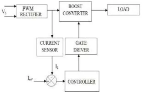
The closed loop control of boost converter involves thecomparison of the reference current with the input current to obtain the desired wave shape of current at the input side of the rectifier.
Fig-3: Circuit diagram of closed loop control
This control method of the control system is implemented as follows:
1) Detection of the instantaneous fundamental component of
the voltage and current. Using the second-order Butterworth digital filtering algorithmic program of equation 1, the amplitude, part and frequency characteristics of this filter is shown in figure 4.
Fig-4: The amplitude, phase and frequency characteristics of Butterworth band-pass filter
From which we can see, amplitude of the fundamental component part of the signal doesn't decay, the phase does not shift, that on the idea of guaranteeing filters the DC element of the input signal and high harmonics [4].
2) Calculate the instantaneous active power and reactive power. get the input active power and reactive power via. the calculation of equation 1 and equation 2
p = Ua * Ia +Ub * Ib (1)
q = (Ua +Ub) / √3 (2)
3) For reactive power q, the use of the inner PI control algorithm makes the input reactive power of the rectifier is zero, which achieve the unity power factor input. The diagram to attain the inner PI management rule is shown in Figure 5.
Fig-5: The open loop PI controller of power factor
4) For the DC voltage across the capacitor, use of the outer PI control algorithm and adjust the output DC voltage across the capacitor of the rectifier, thus control the output power. The diagram to attain the outer PI management formula is shown in Figure 6 [4].
Fig-6: The closed loop PI controller of power
5) Obtain the real-time phase of the grid. The three-phase basic voltage got in Step 1 will obtain the period of time section data of the grid by mistreatment formula 3, formula 4 and formula 5 [5].
(3)
(4)
© 2019, IRJET | Impact Factor value: 7.211 | ISO 9001:2008 Certified Journal
| Page 5983
III. THE SIMULATION OF PWM RECTIFIER SYSTEM ANDITS POWER FACTOR CONTROL
Fig-7: Simulink model with subsystems
The Simulink model was created for the design parameters and the output was captured in order to get the desired output. The Simulink model includes the following sections, the input rectifier, boost converter, reference current generation and the PI controller. Shown in fig 7.
The Simulink model for the prototype consists of subsystems.
Fig-8: Controller Subsystem
The controller subsystem consists of the power factor must be improved at the input stage.
Fig-9: Reference current generation
The major idea of the reference current generation is to create a logic which would eventually generate a current like that of the input current with respect to that of an input voltage.
The reference current can be calculated by for this expression:
Input source voltage is given by,
, (5)
This Vs is normalized and rectified to obtain,
This equation is the normalized and rectified source voltage waveform, defines the reference current wave shape. The amplitude is determined by the output power. If Po is the output power, then
; (6)
Assuming 100% efficiency of the boost converter,
(7)
This determines the amplitude of the reference current wave shape.
The reference current is given as,
(8)
This rectifier is followed by the boost converter which is involved in the process of current shaping. The current in the inductor is adjusted by adjusting the duty cycle of the MOSFET.
© 2019, IRJET | Impact Factor value: 7.211 | ISO 9001:2008 Certified Journal
| Page 5984
wave in order to generate the output pulses for the gatedriving circuit
IV.SIMULATION RESULTS
The results at every step of the Simulink model has been recorded and the obtained results are as per expectations. Figure.10 depicts the input current waveform without a controller whose wave shape must be corrected in order to obtain a unity power factor.
After the application of the reference current generation logic the reference current generated has been in accordance with the input current of the rectifier which is the desired output. Figure 11. shows the obtained reference current.
Fig-10: Input Current waveform without controller
One point to be noted is that the reference current generated is based on the output voltage and current of the boost converter. Also, logic involves the use of the power requirement of the application desired. In order to obtain the better-closed loop control, the output voltage, current, and the power requirement must be known.
Fig-11: Reference current generated
The boost converter acts as a major part in PFC where the inductor controls the current from the rectifier and eventually the unity power factor is obtained. The various parameters of the Boost converter were designed using the simulation of the boost converter is designed.
Fig-12: Output from the boost converter
The output constant value of the PI controller is compared with the triangular wave and the result is a square wave which is used as a pulse to drive the MOSFET.
Fig-13: Pulse to the MOSFET with controller
With the pulse as in figure 13, the MOSFET is driven and the duty cycle of the pulse is varied according to the error generated and the power factor is brought close to unity which is shown in figure 14.
© 2019, IRJET | Impact Factor value: 7.211 | ISO 9001:2008 Certified Journal
| Page 5985
The major objective of the closed-loop control is theimprovement of power factor to about unity to reduce the THD in the input side of the converter. Every sensor used has a scaling factor in order to obtain the correct output. In that sense, the voltage sensor works on the principle of voltage divider circuit and the dividing resistance is taken as the scaling factor. Likewise, for the current sensor, the current obtained in terms of voltage is converted into the current with the help of the scaling factor as specified in the datasheet.
Fig-15: Comparison Of Power Factor
The comparison of power factor obtained in hardware is given in table 1.
Table-1: comparison of Power factor
Open Loop Control Closed Loop Control
0.6667 0.9997
Hence, it could be inferred that the major objective of power factor correction has been achieved to a major extent with closed loop control.
V.CONCLUSION
Thus, the development of the boost converter topology to improve the source power factor for an AC-DC converter(rectifier) has been designed. The simulation model, design and control logic of the boost power factor correction converter have been incorporated. The inductor in the boost converter is very much advantageous for this development wherein the inductor itself helps in shaping the current, rather than other converters where an additional switching circuit is necessary. There is also a better reduction of harmonics in comparison with the front end. Also, since the inductor at the boost converter causes low inductor ripple and other distortions, the basic objective of the project is satisfied. Also, the other objectives like that of a driver circuit design and PI control have been fulfilled.
REFERENCES
[1] Devan Junesco, Shahad AL-Youif , “Passive Filter
Design Proposed For Harmonic Extenuation”, International Journal Of Engineering And Technology,vol:7,pp 75-84,2013
[2] A.InbaRexy, R.Seyezhai, “A Comparative Study of
Active Power Factor Correction AC-DC Converters for Electric Vehicle Applications”, ARPN Journal of Engineering and Applied Sciences, Vol 8, No 9, PP 727-732, Sep 2013.
[3] I.SudhakarBabu, Dr.G.V.Siva Krishna Rao, “Active
Power Factor Correction Using Boost Converter”, International Journal of Science,Engineering and Technology Research(IJSETR), Vol 3, PP 2755-2759, Oct 2015.
[4] HitenPahilwani, “Power Factor Correction Using
Boost Converter”, International Journal of Application or Innovation in Engineering and Management(IJAIEM), Vol 4, PP 134-140,Aug 2015.
[5] D.S.Chen, J.S.Lai , “Power Factor Correction using