Reducing neutral point voltage fluctuation in NPC
three-1
level active power filters
2
Peng Qian 1* Xiandong Ma 1 Guohai Liu 2 Zhaoling Chen 2
3
1 Engineering Department, Lancaster University, Lancaster LA1 4YW, United Kingdom; p.qian @lancaster.ac.uk,
4
5
2 College of Electrical and Information Engineering, Jiangsu University, Zhenjiang, China; [email protected],
6
7
* Correspondence: p.qian @lancaster.ac.uk;Tel: +44 (0)1524 593700
8
Abstract: Shunt active power filters (SAPFs) have been widely used to improve power quality of the grid by
9
mitigating harmonics injected from nonlinear loads. This paper presents a new method for improving the
10
performance of SAPFs using neutral point clamped (NPC) three-level inverters. NPC three-level inverters
11
often suffer excessive voltage fluctuations at the neutral-point of DC-link capacitors, which may damage
12
switching devices and cause additional high harmonic distortion of the output voltage. In order to solve the
13
problem, two compensating schemes are proposed to restrict voltage fluctuation in the inverters. The first is
14
voltage dependent, adopting a voltage compensation method, while the second is current dependent, using a
15
current compensation method. The paper describes the respective circuit architectures and principles of
16
operation. Corresponding models are mathematically formulated and evaluated under typical balanced and
17
unbalanced working load conditions. The results show that both schemes are able to alleviate considerably
18
voltage oscillations and hence harmonic distortions, and the current compensated NPC inverter outperforms
19
the voltage compensated NPC inverter. Consequently, it is shown that the proposed approaches are effective
20
and feasible for improving power quality of the grid when connected to nonlinear loads.
21
Keywords: shunt active power filter (SAPF), three-level inverter, neutral point clamped (NPC), DC-link,
22
voltage compensation, current compensation
23
24
Symbols and abbreviations
25
SAPF Shunt active power filters
26
NPC Neutral point clamped
27
DG Distributed generation
28
PV Photovoltaics
29
THD Total harmonic distortion
30
SVPWM Space voltage vector pulse-width modulation
31
VNPCI Voltage dependent NPC three-level inverter
32
CNPCI Current controlled NPC three-level inverter
33
IGBT Insulated gate bipolar transistor
34
usa, usb, usc Three-phase alternating-current supply
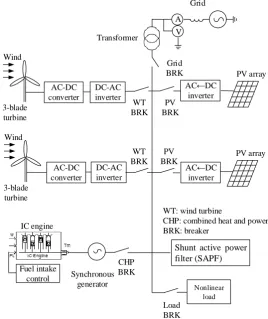
35
isa, isb, isc Grid currents
36
iLa, iLb, iLc Load currents
37
ica, icb, icc Compensation currents provided by the SAPF
38
uo Neutral point voltage of the three-phase bridge arm
39
uN Neutral point voltage of the DC-link capacitors
40
uc Voltage of the primary side of the transformer
41
ub Compensating voltage
42
us DC-link voltage applied across the capacitors
43
S1, S2, S3, S4 IGBTpower switches
44
T Coupling transformer
45
L, Cf LC filter
46
udc DC voltage applied to the single-phase full-bridge inverter
47
ui Voltage output of the single-phase inverter
48
i1 Current through the filter inductor
49
i2 Transformer primary side current
50
icf Current through the filter capacitor
51
D1 Diode used to prevent reverse current flow
52
L2, C3 LC filter
53
udc1 Voltage input of the boost DC/DC converter
54
udc2 Voltage output of the boost DC/DC convertor
ic3(off) Current in capacitor C3 when switching device S5 is turned off
56
i3 Current in the inductor L1
57
i4 Compensating current
58
uL1(off) Voltage across the inductor L1 when switching device S5 is turned off
59
uL1(on) Voltage across inductor L1 when switch S5 is turned on
60
D Duty cycle of the switching device S5
61
Kp, Ki Parameters of the PI controller
62
63
1. Introduction
64
Recently, distributed generation (DG) installation has been significantly increased, due to the deregulation
65
of utilities, environmental constraints, and concerns regarding climate change [1]. This type of power generation
66
system, as shown in Fig. 1, can provide electric power at or on a site closer to end users. However,
harmonic-67
related problems have become a key concern because DG generators, such as wind and photovoltaics (PV), are
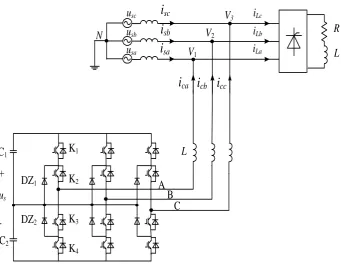
68
coupled to power electronic converters and nonlinear loads [2]. In this regard, shunt active power filters (SAPFs)
69
are widely used to mitigate these harmonic distortion problems in the grid. Compared to traditional two-level
70
voltage-source inverters used in SAPFs, three-level voltage-source inverters are able to bear higher voltage
71
classes and operate with lower harmonic distortion and at lower switching frequencies. Three-level inverters
72
therefore offer better performance, in particular for medium-voltage applications [3]. In terms of topological
73
structure, three-level inverters can be classified as one of three distinct types, namely diode clamped multilevel
74
inverters, clamping capacitor multilevel inverters, and isolated H-bridge multilevel inverters [4-5]. The neutral
75
point clamped (NPC) three-level inverter [6] is classified as type of diode clamped multilevel inverters. The
76
most commonly used NPC three-level inverter circuit [7-9] is shown in Fig. 2, where it is incorporated into a
77
SAPF. A full description of the circuit will be given in subsequent sections.
78
3-blade turbine Wind
DC-AC inverter AC-DC
converter
3-blade turbine Wind
DC-AC inverter
PV array AC DC
inverter
PV array V
A
Transformer
IC engine
Fuel intake
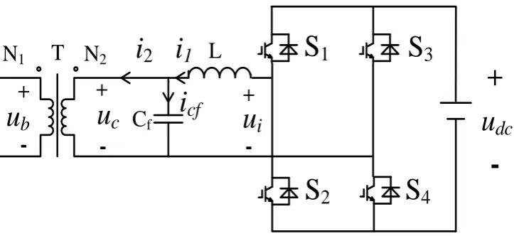
control Synchronous
generator
Grid BRK
Shunt active power filter (SAPF)
WT BRK
WT BRK
PV BRK
PV BRK
CHP BRK
Grid
Nonlinear load
Load BRK AC-DC
converter
WT: wind turbine
CHP: combined heat and power BRK: breaker
AC DC inverter
[image:2.595.171.440.395.715.2]79
Figure 1. Schematic diagram of a distributed generation system
80
81
In a NPC level inverter, the neutral point of the DC-link capacitors and the neutral point of the
three-82
phase bridge circuit are linked together directly. The neutral-point voltage of the three-phase bridge arm will
83
there is a neutral-point current flowing into or out of the neutral points in the circuit [10-11]. The varying current
85
causes a charge-discharge phenomenon associated with the capacitors through the neutral-points in the circuit,
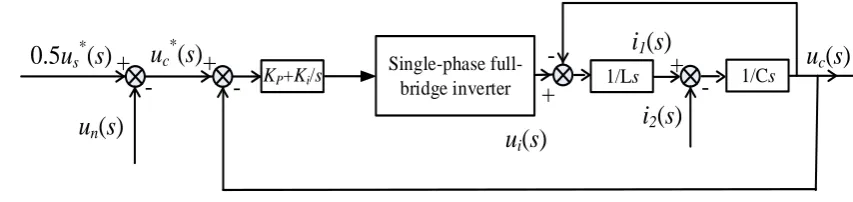
86
thus resulting in a fluctuation in the neutral-point voltage. Consequently, the voltage ripples produced will affect
87
the capability of the NPC three-level inverter to work efficiently [12]. Furthermore, excessive fluctuations of
88
the DC-link voltage increase voltage stresses on the switching devices and hence the total harmonic distortion
89
(THD) of the output current, which may limit potential engineering applications of this type of inverter.
90
There are three main factors that may cause oscillations in the neutral-point voltage in the DC-link branch.
91
Firstly, the capacitance associated with the DC-link capacitors may become unbalanced after use for extended
92
periods of time. DC link capacitors are required to endure high ripple currents leading to self-heating, which,
93
in addition to high ambient operating temperatures, can result in the deterioration of the electrolyte material and
94
the loss of electrolyte by vapour diffusion. Secondly, a critical factor for the inverter to work is delivery of the
95
gate drive signals to the switching devices, as controlled by the switching frequency. Any switching delay will
96
cause load current imbalance. Thirdly, nonlinear loads also cause harmonics to appear in the load current, which
97
may in turn inject harmonics back to the inverter. Mathematical descriptions regarding the causes of voltage
98
oscillations can be found in [13].
99
In order to solve these problems, three main methods have been investigated to alleviate voltage
100
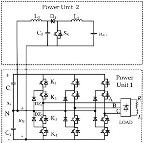
oscillations. The first is through the use of two independent DC sources to ensure a stable and constant DC
101
voltage across the inverter. The method is expensive [14], because two independent DC sources require two
102
isolation transformers. The second involves the design of improved control strategies, which are arguably the
103
most widely used techniques at present [15-17]. Among the control strategies, the best known is the space
104
voltage vector pulse-width modulation (SVPWM) method [18-22]. The control strategy proposed in [18]
105
replaces the P-type or N-type small switching states with other switching states that do not affect the
neutral-106
point voltage. Reference [23] demonstrates the ability of the SVPWM method to balance the neutral point
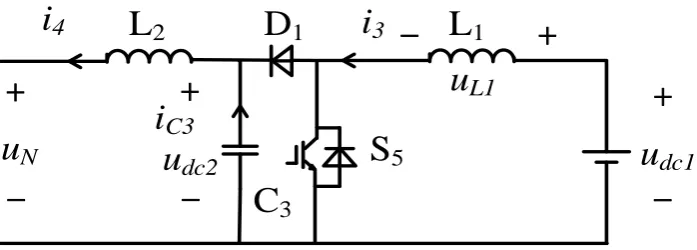
107
voltage for different regions of the space vector plane, while a new general model was introduced in [24] to
108
investigate the theoretical and practical limitations of the balancing problems caused by space vector
109
modulation. A control scheme based on a virtual space vector PWM method is proposed in [25] to control the
110
neutral-point voltage fluctuation over the full range of the modulation index and load power factor, subject to
111
the condition that the sum of the three-phase output currents equals zero. The third method reduces voltage
112
oscillations through a change in circuit topology, as the solution by hardware circuit has its own advantages.
113
This method incorporates auxiliary components in the traditional NPC three-level inverter circuit and has
114
proved to be able to achieve good performance to suppress excessive neutral-point voltage fluctuation
115
effectively at low cost [26].
116
In this paper, two new NPC three-level inverter topologies are proposed. The first is a voltage dependent
117
NPC three-level inverter (VNPCI), which adopts a voltage compensation method to restrain the neutral point
118
voltage fluctuation of the DC-link. The second method is a current controlled NPC three-level inverter (CNPCI)
119
and uses a current compensation method. Both two new inverter topologies are incorporated in a SAPF. The
120
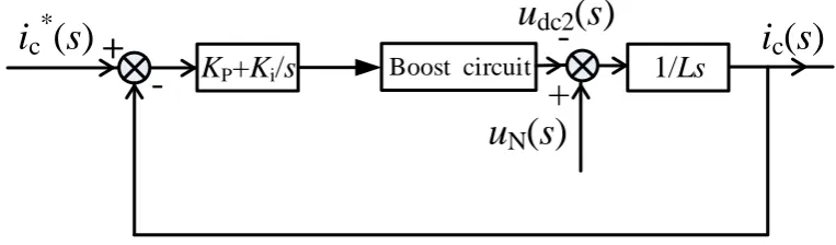
remainder of this paper is organised as follows. The principle of the SAPF is described in Section 2. The circuit
121
architectures, their principles of operation and mathematical models describing voltage and current dependent
122
inverters are outlined in Section 3 and Section 4, respectively. Simulation results of the inverter models and the
123
performance of the SAPF under typical balanced and unbalanced working load conditions are shown and
124
discussed in Section 5. Conclusions and suggestions for future work are given in Section 6.
125
126
C
1C
2DZ
1DZ
2K
1K
2K
3K
4A
B
C
N
R
L
L
V
3V2
V1
u
scu
sbu
sai
sci
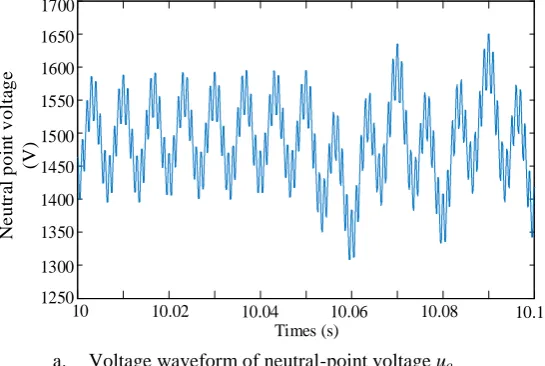
sbi
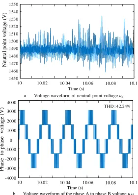
sai
Lci
Lbi
Lau
s+
-i
cai
cbi
cc [image:4.595.130.472.73.337.2]128
Figure 2. A SAPF based on the neutral point clamped (NPC) three-level inverter
129
130
Figure 2 shows a SAPF based on the NPC three-level inverter. In this figure, usa, usb, usc are the
three-131
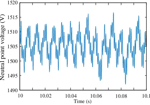
phase alternating-current supplies; the load is nonlinear, generating harmonic currents; isa, isb, isc and iLa, iLb, iLc
132
are grid currents and load currents, respectively; ica, icb, icc are compensation currents provided by the SAPF,
133
which are used to eliminate harmonic currents in the grid. The SAPF is essentially composed of two major
134
components, namely a conventional NPC three-level inverter and an associated control scheme. In the inverter
135
circuit, K1, K2, K3, K4 are IGBT(insulated gate bipolar transistor) power switches, while DZ1, DZ2 are clamp
136
diodes; note that only the components of one inverter arm are labeled for simplicity. The DC bus voltage is split
137
in half using two DC capacitors, C1 and C2, and into three voltage levels, us,0, and -us, via clamping diodes.
138
The control scheme detects the load currents in real time, which are used to calculate command signals for the
139
IGBT switches. The inverter then works as a signal amplification circuit, producing appropriate compensation
140
currents. This compensation current is equal but opposite to the harmonic currents, which can be overlaid to the
141
load currents, thus eliminating the harmonic currents generated by the nonlinear load.
142
143
3. Voltage compensated NPC inverter (VNPCI)
144
3.1. Inverter circuit
145
The schematic diagram of the VNPCI circuit is shown in Fig. 3. Essentially, the circuit consists of two
146
parts. Power unit 1 is associated with the conventional NPC three-level inverter, as described in the preceding
147
section. In order to reduce excessive neutral-point voltage fluctuations across the DC-link capacitors, this paper
148
considers the application of an active voltage compensation method in which the controllable voltage source is
149
used in series between the neutral point of the DC-link and the neutral point of the three-phase bridge circuit.
150
This voltage source is used in order to compensate for voltage fluctuations across the three-phase bridge arm of
151
the inverter. The voltage at the neutral-point of the three-phase bridge arm is detected in real time and compared
152
with a reference voltage, producing an appropriate value for the compensation voltage. Subsequently, the
153
voltage source generates an equal but opposite voltage, thus reducing the voltage fluctuation across the inverter.
154
Power unit 2 is an active voltage compensation device, which in essence is a single-phase full-bridge
155
inverter. The device works as a controllable voltage source and is connected in series between the neutral point
156
of the three-phase bridge arm and the neutral point of the DC-link through a coupling transformer. The variables
157
uo and uN denote the neutral point voltage across the three-phase bridge arm and the DC-link capacitors,
158
respectively; ucand ub are the voltages across the primary and secondary sides of the transformer, respectively,
159
for which ub is used as the compensating voltage; us is the DC-link voltage applied across the capacitors.
161
L
C
fC
1C
2DZ
1DZ
2K
1K
2K
3K
4N
A
N
1N
2B
C
Power Unit 2
Power
Unit 1
+
-u
N+
-u
sS
1S
2S
3S
4O
+
-u
o+
-+
-u
bu
cu
dcLOAD
R
L
[image:5.595.137.461.96.427.2]162
Figure 3. Schematic diagram of the voltage compensated NPC inverter
163
3.2. The active voltage compensation device
164
+
u
dc
L
C
fT
-N
1N
2+
u
i
-u
c
+
-i
2
i
1
i
cf
S
1
S
2
S
3
S
4
u
b
+
-165
Figure 4. Schematic diagram of the active voltage compensation device
166
The voltage compensation device is shown in Fig. 4. It is composed of a single-phase, full-bridge inverter
167
circuit, where S1, S2, S3, S4 are IGBTpower switches; T is the coupling transformer with a transformation ratio
168
of n; the inductor L and the capacitor Cf form a LC filter that removes unwanted switching harmonics from the
169
inverter output.
170
Now consider the mathematical model of the voltage compensation device. In the circuit illustrated in Fig.
171
4, udc is a DC voltage applied to the single-phase full-bridge inverter; uiis the voltage output of the single-phase
172
inverter; i1 is the current through the filter inductor; i2 is the transformer primary side current; icf is the current
173
passing through the filter capacitor.
174
[image:5.595.120.482.470.636.2]n
L
b
1 i
=
di
u
u
-dt
(1)176
Hence, for the NPC inverter shown in Fig. 3, the voltage due to the introduction of the compensating
177
voltage ub can be obtained via the following equations. In the ideal situation, three-phase bridge arm voltage uo
178
should be equal to the half DC-link voltage, i.e., 0.5 us.
179
N
-
b ou
u = u
(2)180
n
L
0.5
N
1
i s
-
di
)
u
(u -
=
u
dt
(3)181
For the voltage output of the single-phase inverter ui
182
*
i dc
u
S u
(4)183
where S* represents the switching function; if S
1 and S4 are switched on whileS2 and S3 are switched off, then
184
S*=1; if S
1 and S4 are switched off while S2 and S3 are switched on, then S*=-1.
185
Substituting (4) into (3) gives
186
*
n( - L )= 0.5
N
1
s dc
- di
u S u u
dt (5)
187
Therefore, the state equations of this active voltage compensation device can be described as,
188
f
1
= ( - ) C
c
1 2
du
i i
dt (6)
189
1
= ( - )
L 1
i c
di
u u
dt (7)
190
The resulting control scheme of the active voltage compensation device is shown in Fig. 5. It illustrates
191
the operating principle of active voltage compensation device as controlled by this scheme. In this diagram, the
192
voltage 0.5us*(s) refers to half of the DC-link voltage under balanced capacitors; un(s) is the DC-link
neutral-193
point voltage measured in real time; uc*(s) is the reference compensating voltage; ui(s) is the output voltage of
194
the single phase full bridge inverter circuit; uc(s) is the transformer primary side voltage; i1(s) is the current in
195
the filter inductor; and i2(s) is the transformer primary side current. The compensating voltage uc*(s) is obtained
196
by calculating the difference between the measured neutral-point voltage of link and half of the ideal
DC-197
link voltage. The error voltage between uc*(s) and uc(s) is then used for generating PWM signals based on the
198
triangular wave modulation method, which are then used to control the voltage output of the single-phase
199
inverter at a desired level. A PI controller, represented by Kp+Ki/s, is used because it can provide a compensating
200
voltage output more accurately, thus improving performance further.
201
un
(
s
)
0.5
us
*(
s
) +
-
+
-
KP+Ki/suc
*(
s
)
+
-uc
(
s
)
Single-phase
full-bridge inverter 1/Cs
i1
(
s
)
i2
(
s
)
1/Ls
+
-ui
(
s
)
[image:6.595.79.506.535.636.2]202
Figure 5. The control scheme for the active voltage compensation device
203
4. Current compensated NPC inverter (CNPCI)
204
4.1. Inverter circuit
205
As described above, the primary reason causing neutral-point voltage fluctuation across the DC-link is the
206
current that flows in to or out of the neutral points in the circuit. The varying current will lead to
charge-207
discharge phenomena associated with the capacitors through the neutral-points in the circuit, resulting in a
208
fluctuation in the neutral-point voltage. The voltage fluctuation can be alleviated naturally through the use of
209
an active current compensation scheme in which a controllable current source is connected in shunt with one of
210
neutral point of DC-link capacitors and the neutral point of three-phase bridge circuit. It can further suppress
212
neutral-point voltage fluctuations because, if this scheme is applied effectively, there is approximately zero
213
current flowing between the neutral points in the inverter.
214
215
216
L
1C
1C
2DZ1
DZ2
K
1K
2K
3K
4A
B
C
Power Unit
2
Power
Unit 1
+
-u
sS
5N
+
-u
N LOADL
2u
dc1D
1C
3R
L
[image:7.595.157.453.137.430.2]217
Figure 6. Schematic diagram of the current compensation NPC inverter
218
219
The schematic diagram of CNPCI is shown in Fig. 6. It also consists of two parts: part 1 is the conventional
220
NPC three-level inverter and part 2 is the proposed active current compensation device. The compensation
221
device is essentially a boost DC/DC conversion circuit, which works as a current source. The current flowing
222
between the neutral points of the inverter is detected in real time, and an equal but opposite current is then
223
generated through the current compensation device, offsetting the current flow between the neutral points in the
224
inverter. Thus, the charge-discharge phenomenon of DC capacitors through DC-link neutral-point can be
225
restrained effectively. The effectiveness of the current compensation device relies on the voltage difference
226
between the boost circuit and the DC-link, which is applied to the inductor (L2 in Fig. 6), thus producing a
227
compensation current for the DC capacitor.
228
229
4.2. Inverter circuit
230
L
1
S
5
L
2
D
1
[image:8.595.125.474.77.202.2]+
u
dc1
-C
3
i
3
i
4
u
dc2
+
-+
-u
N
+
-u
L1
i
C3
232
Figure 7. Schematic diagram of the active current compensation device
233
Fig. 7 shows the proposed active current compensation device, essentially a boost DC/DC converter
234
circuit, where S5 is the IGBT power switch; D1 is a diode preventing reverse current flow; L1 is a power inductor
235
used for energy storage; L2 and C3 form a LC filter for the circuit. Now consider the mathematical model of the
236
active current compensation device. In the circuit, udc1 is the voltage input of the boost DC/DC converter; udc2
237
is the voltage output of the boost DC/DC convertor; uN is the DC-link neutral-point voltage; ic3 is the current in
238
the capacitor C3; i3 is the current in the inductor L1; i4 is the compensating current. Suppose ic3(off)andic3(on)are
239
the current in capacitor C3 when the switching device S5 is off and on, respectively; uL1(off) is the voltage across
240
the inductor L1 when the switching device S5 is off while uL1(on) is the voltage across the inductor L1 when the
241
switch S5 is on.
242
When the switching device S5 is turned on, the state equations of the current compensation device can be
243
described as,244
1 (on) 3 (on)L
C
1 3 3 dc1 L dc2 4 Cdi
= u
= u
dt
du
= i = i
dt
(8)245
When the switching device S5 is turned off, the above equation can be writen as
246
1 (off) 3 (off)L
C
1 3 3dc1 dc2 L
dc2
4 3 C
di
= u
- u
= u
dt
du
= i - i = i
dt
(9)247
During one switching cycle, TS, the average voltage across the inductor L1 is,
248
1
s s
1
1 s 1
t+DT t+T
L L on L off
t t+DT
S
u =
u
τ dτ +
u
τ dτ
T
(10)
249
1
1
L dc1 dc1 dc2
u = Du
+ - D u
- u
(11)
250
where D represents the duty cycle of the switching device S5, i.e., the proportion of time during which S5 is
251
operated.
252
During one switching cycle, the average current in the capacitor C3 is equal to
253
1
s s
3 3 3
s
t+DT t+T
C C on C off
t t+DT
S
i =
i
τ dτ +
i
τ dτ
T
(12)
254
1
3
C 4 4 3
i
= Di +
- D i - i
(13)
255
It is well known that the average voltage across an inductor and the average current in a capacitor should
256
be zero during a switching cycle. Hence, under steady state, the current compensation device can be described
257
1
1
1
dc2 dc1
4 3
u
=
u
- D
i =
- D i
(14)
259
A control scheme, designed for the active current compensation device, can be derived from this model,
260
as shown in Fig. 8. In this circuit, udc2(s) is the voltage output of the boost DC/DC converter; uN(s) is the
DC-261
link neutral-point voltage measured in real time. The reference compensating current ic*(s) is obtained by the
262
real-time detection of the current flowing between the neutral points of the inverter. The current ic(s) is the
263
compensation current generated by the boost circuit. The error currentbetween ic*(s) and ic(s) is then used to
264
generate PWM signals. This signal is based on the triangular wave modulation method, producing a
265
compensating current at the desired level. As with the voltage compensation scheme, a PI controller, represented
266
by Kp+Ki/s, is used because it generates a more accurate compensation current.
267
+
-
K
P+
K
i/
s
i
c
*
(
s
)
i
c
(
s
)
Boost circuit
u
N
(
s
)
1/
Ls
+
-u
dc2
(
s
)
[image:9.595.103.485.240.352.2]268
Figure 8. The control scheme for the active current compensation device
269
5. Results and analysis
270
5.1. The inverters
271
Models of the voltage compensation device and the current compensation device have been built using
272
Simulink SimPowerSystems, as described above and shown in Fig. 3 and Fig. 6, respectively. The parameters
273
used in the models are given in Table 1. The DC-link voltage is 3 kV, a level commonly used in medium voltage
274
power drives; the switching frequency for the NPC three-level inverter is 1 kHz; and the switching frequencies
275
used to control the single-phase inverter for the voltage- and current-compensation device are both set to 10
276
kHz. In order to evaluate the dynamic performance of the proposed inverters, a nonlinear load is used in this
277
study. This load consists of a three-phase rectifier with a resistive (4Ω) and inductive (15mH) load. The use of
278
a nonlinear load increases the neutral-point voltage fluctuation of the DC-link, because the nonlinear load draws
279
a current that is not necessarily sinusoidal, hence generating harmonic currents. The NPC three-level inverter
280
is used with a constant voltage output control strategy, based upon space voltage vector modulation (SVPWM).
281
The error voltage between the NPC three-level inverter output voltage and the reference voltage is processed
282
by a PI controler, which is then used as the input signal for SVPWM to generate appropriate PWM signals. This
283
control scheme has a higher eficiency for controlling the DC-side voltage than the equivalent sine pulse width
284
modulation method.
285
Table 1. Parameters used in the VNPCI and CNPCI inverters
286
Parameters of the VNPCI Parameters of the CNPCI
Parameters Value Parameters Value
udc 500 V udc1 100 V
Cf 50 μF L1 10 mH
L 0.4 mH L2 0.5 mH
C3 800 μF
Parameters of the NPC three-level inverter
us 3000 V
[image:9.595.139.459.632.786.2]287
In real world applications, the load can be either in a balanced or unbalanced condition. An unbalanced
288
load added to the three phase output voltage of an inverter can result in greater fluctuations in the neutral-point
289
voltage across the DC-link. In the simulation, the inverters are initially connected to a balanced nonlinear load,
290
and resistive (8Ω) and inductive (1.5mH) loads are then applied between phase A and phase B in order to
291
evaluate the dynamic performance of the proposed compensation devices under a unbalanced load condition.
292
The unbalanced load occurs at 10.05 s and lasts for 0.05 s.
293
Firstly, a conventional NPC three-level inverter, under balanced and unbalanced working load conditions,
294
has been modelled and investigated. Fig. 9(a) and (b) show the waveform of the neutral-point voltage uo, the
295
phase A to phase B voltage uAB of the conventional inverter. The neutral-point voltage fluctuation across the
296
DC-link is severe, even in the balanced load condition; the range of the fluctuation reaches a value of 200V.
297
During the unbalanced load condition, applied from 10.05s to 10.1s, it can be seen the neutral-point voltage
298
fluctuation range increases to 300V. The THD (total harmonic distortion) of the output voltage waveform across
299
the inverter is 45.30%.
300
301
Times (s)
N
e
u
tr
al
p
o
in
t
v
o
lt
ag
e
(V
)
1250 1300 1350 1400 1450 1500 1550 1600 1650 1700
10 10.02 10.04 10.06 10.08 10.1
302
a. Voltage waveform of neutral-point voltage uo
303
304
10 10.02 10.04 10.06 10.08 10.1
4000
3000
2000
1000
0
-1000
-2000
-3000
-4000
Time (s)
P
ha
se
t
o pha
se
v
ol
ta
ge
(
V
)
THD=45.30%305
b. Voltage waveform of phase A to phase B voltage uAB
[image:10.595.167.446.271.656.2]306
Figure 9. Voltage waveforms of the conventional NPC in a load swell
307
Fig. 10(a) and (b) show the waveform of the neutral-point voltage uo, the phase A to phase B voltage uAB
308
of the proposed voltage compensated NPC inverter under the balanced and unbalanced working load conditions.
309
With the voltage compensation device being added, the neutral-point voltage fluctuation of DC-link is
310
suppressed effectively, being reduced to 40V. Similarly, an unbalanced load is applied at 10.05 s, lasting 0.05
311
s. The neutral-point voltage fluctuation of DC-link is reduced to 75V under the unbalanced load condition. The
312
[image:10.595.171.444.273.456.2]10 10.02 10.04 10.06 10.08 10.1 1550
1540
1530
1520
1510
1500
1490
1480
1470
1460
1450
N
eut
ra
l poi
nt
v
ol
ta
ge
(
V
)
Time (s)
314
a. Voltage waveform of neutral-point voltage uo
315
10 10.02 10.04 10.06 10.08 10.1
4000
3000
2000
1000
0
-1000
-2000
-3000
-4000
P
ha
se
to p
ha
se
v
ol
ta
ge
(
V
)
Time (s)
THD=42.24%
316
b. Voltage waveform of the phase A to phase B voltage uAB
317
Figure 10. Voltage waveforms of the proposed VNPCI in a load swell
318
319
Fig. 11(a) and (b) shows the neutral-point voltage uo, the phase A to phase B voltage uAB of the proposed
320
current compensated NPC inverter under the balanced and unbalanced working load conditions. With the
321
current compensation device being added, the neutral-point voltage fluctuation of DC-link is suppressed further
322
to 18V. Under the unbalanced load condition between 10.05 s and 10.1 s, the neutral-point voltage fluctuation
323
of DC-link is reduced to 25V. The THD of output voltage of the NPC three-level inverter is 42.08%.
324
The results clearly show that the current compensated NPC inverter (CNPCI) has a better performance
325
than the voltage compensated NPC inverter (VNPCI). Fig. 10 and Fig. 11 demonstrate that the CNPCI can
326
restrict the neutral-point voltage fluctuation of the DC-link to 0.6% and 0.83%, respectively, when the CNPCI
327
works under typical balanced and unbalanced working load conditions. However, the VNPCI restrains the
328
neutral-point voltage fluctuation of DC-link to 1.2% and 2.3%, respectively, in the same conditions. The
329
waveform comparison of neutral-point voltage uo produced in different condition is shown in Fig. 12. The effect
330
of the switching frequency on the output performance was also investigated. It was found a frequency higher
331
than 2 kHz can produce acceptable results but the use of 10 kHz switching frequency produced the best results
332
although it might be too fast for the device to work at such a high voltage level.
333
[image:11.595.158.440.73.469.2]10 10.02 10.04 10.06 10.08 10.1 1520
1515
1510
1505
1500
1495
1490
N
e
ut
ra
l poi
nt
v
ol
ta
ge
(
V
)
Time (s)
335
a. Voltage waveform of neutral-point voltage uo
336
4000
3000
2000
1000
0
-1000
-2000
-3000
-4000
P
ha
se
t
o phas
e
v
ol
ta
ge
(
V
)
10 10.02 10.04 10.06 10.08 10.1
Time (s)
THD=42.08%
337
b. Voltage waveform of the phase A to phase B voltage uAB
[image:12.595.181.439.75.255.2]338
Figure 11. Voltage waveforms of the proposed CNPCI in a load swell
339
340
Times (s)
N
e
u
tr
al
p
o
in
t
v
o
lt
ag
e
(V
)
1250 1300 1350 1400 1450 1500 1550 1600 1650 1700
10 10.02 10.04 10.06 10.08 10.1
Conventional NPC inverter
Voltage compensated NPC inverter Current compensated NPC inverter
341
Figure 12. Waveform comparison of the neutral-point voltage uo produced in the three inverter topologies
342
343
The VNPCI only eliminates the voltage fluctuation at the neutral-point of three-phase bridge arm; there is
344
still fluctuation of the neutral-point voltage of the DC-link. This means the fluctuation problem cannot be
345
eliminated thoroughly. However, the CNPCI can eliminate the neutral-point voltage fluctuation of the DC-link
346
[image:12.595.178.442.529.703.2]capacitors and the neutral point of the three-phase bridge circuit in the inverter, which is the cause of the voltage
348
fluctuation. In addition, for the VNPCI, an isolated transformer is required, which should be able to handle
349
several harmonic components without entering to the saturation region in the primary side and handle secondary
350
side voltage range quickly to compensate the zero sequence voltage generated at the NPC converter. A
351
complicated control scheme is therefore needed to overcome these problems [27]. On the contrary, the CNPCI
352
avoids using the isolated transformer; the cost to manufacture and assemble the CNPCI is therefore lower than
353
the VNPCI; the CNPCI requires only one IGBT power switching device (the most expensive component in the
354
circuit), while the VNPCI needs four IGBT power switches and a coupling transformer. Thus, the CNPCI offers
355
a more cost-effective performance.
356
The selection of PI control parameters were made by trial and error, aiming to achieve an optimal
357
performance from tests. The proportional response can be adjusted by multiplying the error (i.e., the voltage
358
difference in the case of the VNPCI and the current difference in the case of the CNPCI) by the proportional
359
gain Kp. The integral term in the PI controller is the sum of the instantaneous error over time, thus giving the
360
accumulated offset, which is then multiplied by the integral gain Ki. For the VNPCI, the selected value of Kp
361
and Ki are 5 and 10, respectively, while, for the CNPCI, the selected value of Kp and Ki are 10 and 0.5,
362
respectively. Results have shown that the use of these parameters can provide an improved performance of the
363
controllers.
364
5.2. The shunt active power filters (SAPF)
365
The two proposed inverters are now applied in the SAPF that is indispensable part of the grid system. The
366
SAPFs incorporating with the current compensated NPC inverter and the voltage compensated NPC inverter
367
have been built and simulated. One of the typical SAPF applications is in the AC 400V DG system [28]; but
368
unlike the normal inverter, in order to satisfy the working condition in three phase power system, the DC link
369
voltage of SAPF must be over 3 times higher than the phase voltage. Thus, the NPC three-level inverter is very
370
suitable to apply in SAPF due to high DC link voltage. The parameters used in the model are defined as follows:
371
DC link voltage of SAPF is 800V; supply fundamental frequency f = 50Hz; filter line inductance Ls= 2mH;
372
other parameters used for the inverters are referred to Table 1. It is noteworthy that the use of a low DC link
373
voltage, rather than the 3000V previously discussed, was to assess the performance of the proposed inverters
374
for this particular application in SAPF. As mentioned above, nonlinear loads are often connected in the power
375
grid and the load condition will affect the work efficiency of the NPC three-level SAPF. The SAPF is firstly
376
connected to a balanced nonlinear load and then to an unbalanced load emulated by a resistive (8Ω) and
377
inductive (1.5mH) load being applied between phase A and phase B. The unbalanced load also occurs at 10.05
378
s and lasts 0.05 s.
379
Firstly, a SAPF based on the traditional NPC three-level inverter connected with the three phase nonlinear
380
[image:13.595.185.432.575.739.2]load, as shown in Fig. 2, has been investigated under the balanced and unbalanced working load conditions.
381
Fig. 13 show the waveform of grid current of phase A, as an example. The grid current distorts heavily in both
382
balanced and unbalanced load condition, and the THD of the grid current is 18.52%.
383
384
10 10.02 10.04 10.06 10.08 10.1
Time (s)
200
150
100
50
0
-50
-100
-150
-200
C
u
rr
en
t
(A
)
THD=18.52%
385
Figure 13. Waveform of phase-A current of the power grid under the nonlinear load
Fig. 14 shows the waveform of the filter output of phase A, i.e., the currents ica, icb and icc as shown in Fig.
387
2, and the grid currents of the proposed VNPCI three-level SAPF, i.e., the currents isa, isb and isc as shown in
388
Fig. 2, under the typical balanced and unbalanced working load conditions. Essentially, the filter output currents
389
are effective to compensate the harmonics being injected from nonlinear loads, hence improving the quality of
390
the gird currents. The frequency component is dominant at 50 Hz while other harmonic components in
phase-391
A current are now eliminated effectively. The THD of the grid current is reduced to 2.05%. Fig. 15 shows the
392
waveform of the grid currents of the proposed CNPCI three-level SAPF under typical balanced and unbalanced
393
working load conditions. It can be seen that the harmonic currents in phase A can be eliminated more effectively.
394
The THD of the grid current is reduced further to 1.7%.
395
396
10 10.02 10.04 10.06 10.08 10.1 -100
-50 0 50 100
Time (s)
C
u
rr
e
n
t
(A
)
397
a. Waveform of the phase-A current in the filter output
398
399
10 10.02 10.04 10.06 10.08 10.1
Time (s) 200
150
100
50
0
-50
-100
-150
-200
C
u
rr
en
t
(A
)
THD=2.05%
400
[image:14.595.170.448.423.598.2]b. Waveform of the phase-A current in the power grid
401
Figure 14. Waveform of the phase-A currents in the filter output and the power grid empolying the
402
proposed VNPCI three-level SAPF
C
u
rr
e
n
t
(A
)
10 10.02 10.04 10.06 10.08 10.1
200
150
100
50
0
-50
-100
-150
-200
Time (s) THD=1.70%
[image:15.595.172.444.76.267.2]404
Figure 15. Waveform of the power grid currents employing the proposed CNPCI three-level SAPF
405
6. Conclusions
406
The paper presents two new NPC three-level inverter topologies in order to eliminate excessive voltage
407
fluctuation happened at the neutral-point of DC-link capacitors of the inverter. The first is voltage dependent,
408
which adopts a voltage compensation method to restrain the neutral point voltage fluctuation. The second is
409
current dependent, using a current compensation method to restrict the voltage fluctuation. The results show
410
that both topologies can suppress the neutral-point voltage fluctuation of the DC-link effectively under typical
411
balanced and unbalanced working load conditions. The current compensated NPC inverter outperforms the
412
voltage compensated NPC inverter. Furthermore, these compensated NPC three-level inverters are applied to a
413
shunt active power filter in the grid lines. It is shown that the proposed approaches are effective and feasible for
414
eliminating harmonic currents and therefore improving power quality of the grid system when connected with
415
nonlinear loads.
416
Future work will focus on experimental testing of the proposed NPC three-level SAPFs to further verify
417
their performance. Optimal selection of PI control parameters for the inverters will also be investigated in order
418
to further optimize system performance under different load conditions. In addition, the application of the
419
proposed current compensated NPC inverter is being considered in both a wind power generation system and a
420
small grid system in the laboratory in order to address the power quality issues related to inverter-coupled
421
generation and associated loads.
422
References
425
1. Pepermans G, Driesen J, Haeseldonckx D, Belmans R, D’haeseleer W. Distributed generation: definition,
426
benefits and issues, Energy Policy 2005; 33: 787-798.
427
2. Pouresmaeil E, Montesinos-Miracle D, Gomis-Bellmunt O, Sudrià-Andreu A. Instantaneous active and
428
reactive current control technique of shunt active power filter based on the three-level NPC inverter,
429
International Transactions on Electrical Energy Systems 2011; 21: 2007-2022.
430
3. Allmeling J H. A control structure for fast harmonics compensation in active filters, IEEE Transactions on
431
Power Electronics 2004; 19(2): 508-514.
432
4. Liang W, Donglai Z, Yi W, Bin W, Hussain S A. Power and voltage balance control of a novel three-phase
433
solid-state transformer using multilevel cascaded H-bridge inverters for microgrid applications, IEEE
434
Transactions on Power Electronics 2016; 31(4): 3289-3301.
435
5. Roodsari B N, Nowicki E P. Fast space vector modulation algorithm for multilevel inverters and its
436
extension for operation of the cascaded H-bridge inverter with non-constant DC sources, IET Power
437
Electronics 2013; 6: 1288-1298.
438
6. Ke M, Frede B. The impact of power switching devices on the thermal performance of a 10 MW wind
439
power NPC converter, Energies, 2012; 5(7): 2559-2577.
440
7. Muyeen S M, Takahashi R, Tamura J. Wind power and hydrogen generation system with cooperatively
441
controlled three-level NPC-VSC based energy capacitor, International Transactions on Electrical Energy
442
Systems 2010; 20: 1071–1081.
443
8. Zaveri T, Bhalja B R, Zaveri N. Load compensation using DSTATCOM in three-phase, three-wire
444
distribution system under various source voltage and delta connected load conditions, International Journal
445
of Electrical Power & Energy System, 2012; 41: 34-43.
446
9. Saad S, Zellouma L. Fuzzy logic controller for three-level shunt active filter compensating harmonics and
447
reactive power, Electric Power Systems Research 2009; 79: 1337-1341.
448
10. Celanovic N, Boroyevich D. A comprehensive study of neutral-point voltage balancing problem in
three-449
level neutral-point-clamped voltage source PWM inverters, IEEE Transactions on Power Electronics 2000;
450
15: 242-249.
451
11. Ui-Min C., Frede B, Kyo-Beum L. Method to Minimize the Low-Frequency Neutral-Point Voltage
452
Oscillations With Time-Offset Injection for Neutral-Point-Clamped Inverters, IEEE Transactions on
453
Industry Applications, 2015; 51: 1678-1691.
454
12. Rodriguez J, Bernet S. A Survey on Neutral-Point-Clamped Inverters, IEEE Transactions on Industrial
455
Electronics 2010; 57: 2219-2230.
456
13. Helle L, Nielsen S M, Enjeti P. Generalized discontinuous DC-link balancing modulation strategy for
three-457
level inverters Power Conversion Conference, Osaka, Japan, 2002; 2: 359-366.
458
14. Yazdani A, Iravani R. Generalized state-space averaged model of the three-level NPC converter for
459
systematic DC-voltage-balancer and current-controller design, IEEE Transactions on Power Delivery, 2005;
460
20: 1105-1114.
461
15. Zaragoza J, Pou J, Ceballos S, Robles E, Jaen C. Voltage-balance compensator for a carrier-based
462
modulation in the neutral-point-clamped converter, IEEE Transactions on Industrial Electronics, 2009; 56:
463
305-314.
464
16. Ui-Min C, June-Seok L, Kyo-Beum L. New Modulation Strategy to Balance the Neutral-Point Voltage for
465
Three-Level Neutral-Clamped Inverter Systems, IEEE Transactions on Energy Conversion 2014; 29:
91-466
100.
467
17. Pulikanti S R, Dahidah S A. Voltage balancing control of three-level active NPC converter using
SHE-468
PWM, IEEE Transactions on Power Delivery 2011; 26: 258-267.
469
18. Ghennam T, Berkouk E M, Francois B. A novel space-vector current control based on circular hysteresis
470
areas of a three-phase neutral point- clamped inverter, IEEE Transactions on Industrial Electronics 2010;
471
57: 2669-2678.
472
19. Lewicki A, Krzeminski Z, Abu-Rub H. Space-vector pulse width modulation for three-level NPC converter
473
with the neutral point voltage control, IEEE Transactions on Industrial Electronics 2011; 58: 5076-5086.
474
20. Xiyou C, Kazerani M. Space vector modulation control of an ac-dc-ac converter with a front-end diode
475
rectifier and reduced dc-link capacitor, IEEE Transactions on Power Electronics 2006; 21: 1470-1478.
476
21. Huibin Z, Finney S J, Massoud A, Williams B W. An SVM algorithm to balance the capacitor voltages of
477
the three-level NPC active power filter, IEEE Transactions on Power Electronics 2008; 23: 2694-2702.
478
22. Bouhali O, Francois B, Berkouk E M. DC link capacitor voltage balancing in a three-phase diode clamped
479
inverter controlled by a direct space vector of line-to-line voltages, IEEE Transactions on Power Electronics
480
2007; 22: 1636-1648.
481
23. Dongsheng Z, Didier G. R. Experimental comparisons of space vector neutral point balancing strategies
482
24. Nikola C, Dushan B. A comprehensive study of neutral-point voltage balancing problem in three-level
484
neutral-point-clamped voltage source PWM inverters, IEEE Transactions on Power Electronics 2000; 15:
485
242-249.
486
25. Sergio B, Josep B, Dushan B, Sergio S. The nearest three virtual space vector PWM—A modulation for
487
the comprehensive neutral-point balancing in the three-level NPC inverter, IEEE Power Electronics Letters
488
2004; 2: 11-15.
489
26. Mishra M K, Joshi A, Ghosh A. Control schemes for equalization of capacitor voltages in neutral clamped
490
shunt compensator, IEEE Transactions on Power Delivery 2003; 18: 538-544.
491
27. Yong L, Yanjian P, Fang L, Denis S, Daniil P, Chonggan L, Long L, Yijia C. A controllably inductive
492
filtering method with transformer-integrated linear reactor for power quality improvement of shipboard
493
power system, IEEE Transactions on Power Delivery, 2016.
494
28. Shengwei L, Yongli L, Jingliao S, Qiang J, Xuguang L. A novel control algorithm for inverter-based
495
distributed generation in unbalanced three phase power systems, International Conference on Sustainable