('
-' '[l1-· 1; IJIGI'T 1
·-too
d.TABLE OF CONTENTS
Introduction . Definitions
Switch Selectable Options Interrupt Priority Chain Status Bit Selection
Interface Options
Register Description .
Operation Using Z80 Interrupts .
Operation Using 8080 Mode Interrupts Connecting the TU-ART to I/O Devices
1 1
2
6
6
8
9
. • . 18
21
. . 26
TU-ART I/O Connectors. . . . . 26 Terminal to TU-ART Cable . . . . . . 31 Originate Mode Modification . . . 32 Spare RS232 Drivers and Receivers . . . 34
Annotated Software Example . . . • • 35
TU-ART Kit Assembly Information • 36
Parts List • • 37
Parts Placement Diagram. • • • 39
Theory of Operation • • • 40
CROMEMCO TU-ART DIGITAL INTERFACE
INTRODUCTION
The Cromemco TU-ART (Twin Universal Asynchronous
Receiver and Transmitter) provides two channels of duplex serial data exchange; two channels of parallel data
exchange; and ten interval timers. Status information
is available through polling or by interrupt. In addition,
each interval timer activates an interrupt and two inter-rupt request lines are brought out for the user. The
TU-ART has its own crystal-controlled clock and interfaces
to the S-100 bus asynchronously so that CPU clock frequency is not critical. The TU-ART incorporates two TMS 5501 Nmos I/O Controller chips.
DEFINITIONS
Throughout this manual the two TMS 5501 chips will be referred to as "Device A" and "Device B". Device A (IC 4)
is the leftmost chip. Device B (IC 5) is the rightmost
chip. Device A is nearer the heat sink and drives serial
connector J4 and parallel connector J2. Device B is
located to the right of Device A and drives serial connector J5 and parallel connector J3.
-SWITCH SELECTABLE OPTIONS
1. Device A Address. The base address of the ports
associated with Device A is set with positions 6-3 of the DIP switch which determine the msb, 2msb, 3msb, and 4msb
of the I/O address. Setting a switch "on" conditions the
TU-ART to respond to a
"0"
in that address bit. The msb, 2msb, and 3msb also control D7, D6, and DS of the TU-ARTs Z80 mode 2 Interrupt Acknowledge Response vector. Address bits A3, A2, AI, and A~ are decoded to select which controlor data port is being accessed (see Figure 2).
2. Device B Address. The base address of the ports associated with Device B is set with positions 10-7 of the DIP switch which determine the msb, 2msb, 3msb, and 4msb
of the I/O address. Setting a switch "on" conditions the TU-ART to respond to a "~" in that address bit.
3. Interrupt Mode. When this switch (position 1) is on, the TU-ART operates in the 8080 interrupt mode:
one of eight "Restart" instructions is gated to the data
, '.,
bus during an Interrupt Ac~nowledge cycle~ Since the TU-ART can interrupt from one of 16 different sourc~s, it is necessary to poll the devices if the TU-ART is in 8080
mode (see page 21 ).
When switch position 1 is off, the TU-ART responds· in
Z80 mode 2. In this mode, the TU-ART supplies a byte to the data bus during Interrupt Acknowledge that is used as
. ~ ~ ... ; : . F: : ': ;
-the lower eight bits of a memory address. The Z80 supplies the upper eight bits from the I register and automatically reads the corresponding memory location, as well as the next location,
to find the starting location of an interrupt routine. Refer to pages 18-20 and/or the ~80 CPU Reference manual for details.
4. Normal/Reverse Address. -When this switch (position 2)
is on, it allows Device A and Device B to swap base addresses by means of an output to one of the parallel ports (Software
Address-Reverse). This allows either Device A or Device B to be driven by a software driver whose port assignments are
frozen in memory. Setting the switch "on" connects the ~sb of
Device A's parallel output port to the Reverse Address control
so ~hat addresses may be flipped under software control. To
flip addresses, output a byte with D7 high to Device A's
paral-lel output port. To return to normal addressing, output a byte with D7 low to Device B's parallel output port. When switch position 2 is off, the Address Reverse switch is disconnected
from the parallel port.
The Address Reverse signal is brought out to pin 1 of J2 and J3. When the Address Reverse switch is on, pin 1 will show
the state of the TU-ART: Pin 1
=
0 means Reverse Mode,Pin 1
=
1 means Normal Mode.When the Address Reverse switch is off, pin 1 of J2 or J3
may be grounded externally to place the TU-ART in reverse Mode (Hardware Address-Reverse). Do not ground pin 1 of J2 or J3
while the Reverse Address switch is on as this will conflict
with operation of Device A's parallel port.
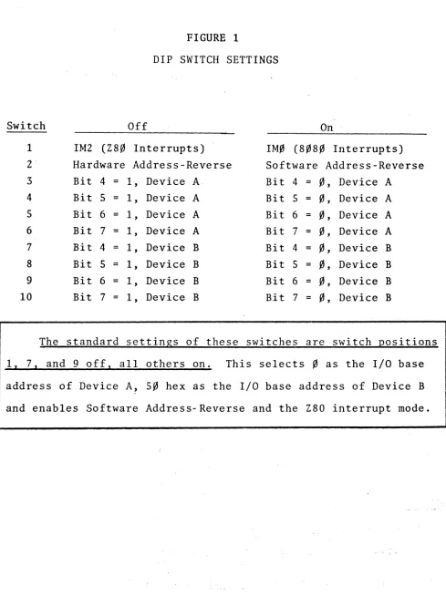
-FIGURE 1
DIP SWITCH SETTINGS
Switch Off On
1 1M2 (Z8~ Interrupts) IM~ (8~8~ Interrupts)
2 Hardware Address-Reverse Software Address-Reverse 3 Bit 4
=
1, Device A Bit 4=
~, Device A4 Bit 5
=
1, Device A Bit 5 = ~, Device A 5 Bit 6 = 1, Device A Bit 6 = ~,
Device A6 Bit 7 = 1, Device A Bit 7 = ~, Device A
7 Bit 4
=
1, Device B Bit 4 = ~, Device B 8 Bit 5=
1, Device B Bit 5=
~, Device B9 Bit 6 = 1, Device B Bit 6
=
~, Device B10 Bit 7 = 1, Device B Bit 7 = ~, Device B
The standard settings of these switches are switch positions
1. 7. and 9 off. all others on. This selects ~ as the I/O base address of Device A, 5~ hex as the I/O base address of Device B
and enables Software Address-Reverse and the Z80 interrupt mode.
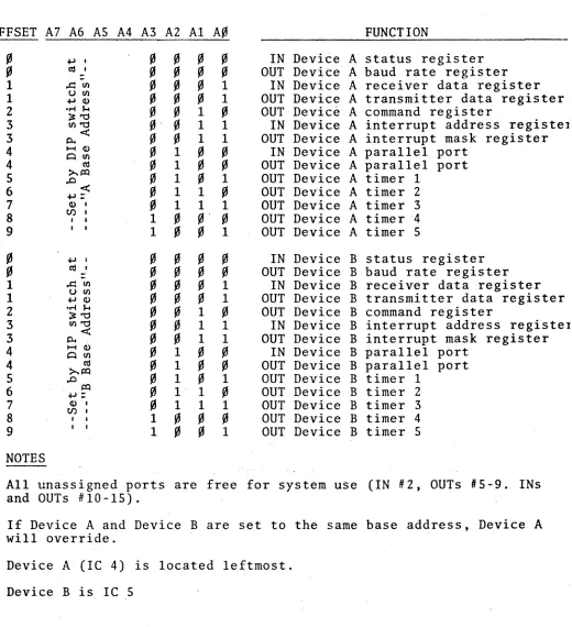
[image:6.612.68.557.73.727.2]-FIGURE 2
SUMMARY OF DATA AND CONTROL PORT ADDRESS FOR TU-ART tm
OFFSET A7 A6 AS A4 A3 A2 Al A~
~ ~ I I 2 3 3 4 4 5 6 7 8 9 ~ ~ I I 2 3 3 4 4 5 6 7 8 9 NOTES ~. CIS' ~. CIS. ,.r::Ul UUl ~(I)
.r! $-4
~"'I:I Ul"'l:l <: Po.. 1-1(1) ~Ul CIS ~/Xl ..0 /Xl ~:
( I ) '
tJ) •
• I
••
FUNCTION
IN Devi~e A status register
OUT Device A baud rate register IN Device A receiver data register OUT Device A transmitter data register OUT Device A command register
IN Device A interrupt address registel OUT Device A interrupt mask register
IN Device A parallel port OUT Device A parallel port OUT Device A timer 1
OUT Device A timer 2 OUT Device A timer 3 OUT Device A timer ·4 OUT Device A timer 5
IN Device B status register OUT Device B baud rate register
IN Device B receiver data register OUT Device B transmitter data register OUT Device B command register
IN Device B interrupt address registel OUT Device B interrupt mask register
IN Device B parallel port OUT Device B parallel port OUT Device B timer 1
OUT Device B timer 2 OUT Device B timer 3 OUT Device B timer 4 OUT Device B timer 5
All unassigned ports are free for system use (IN #2, OUTs #5-9. INs and OUTs #10-15).
If Device A and Device B are set to the same base address, Device A will override.
Device A (IC 4) is located leftmost. Device B is Ie 5
[image:7.612.62.582.141.711.2]INTERRUPT PRIORITY CHAIN
When more than one TU-ART is used in a system, it is necessary to coordinate the Interrupt Responses in order
to prevent bus conflict during Interrupt Acknowledge cycles. This is done by first connecting Jl PRIORITY OUT/ from the
highest priority TU-ART to Jl PRIORITY IN/ of the next highest priority TU-ART , then connecting Jl PRIORITY OUT/ of the second TU-ART to J1 PRIORITY IN/ of the next TU-ART,
and so on- until all TU-ARTs are connected. The J1 PRIORITY IN/ pin of the highest priority board is left unconnected. Device A is internally prioritized over Device B on each TU-ART.
STATUS BIT SELECTION
The connection of status flag bits to data bits is done on the PC board at the location of the status socket below
J3. Cromemco software conventions assign D6=Receiver Data Available (RDA), and D'7=Transmi tter Buffer Empty (TBE). For
specialized assignments (like more than one bit per flag) see
page 7.
Status Socket
The status flag bits available on input port ~ are
con-nected to the data bits by foil traces in the "status socket"
located between IC's 8 and 9.
-The flag assignment used by all Cromemco software is
discussed on page 9 under "Register Description".
If necessary, the flags may be assigned to different data
bits. This may be most easily done as follows:
1. Notice that the flags are arranged along the left
row of pads and that the data bits are arranged along the right side row of pads. Note also 'that only those 8 traces connecting the right and left pads are not covered by the solder mask. There are 5 traces which pass through this area which are covered.
2. Use a razor blade or similarly sharp knife to cut
all 8 of the traces connecting the left and right rows of pads. Be very careful not to cut the traces which
are covered by the solder mask.
3. Install and solder a 16 pin IC socket in the 2 rows
of pads.
4. Install a 16 pin "comporent header" in the socket. S. Using small (24 or 28 Awg) insulated wire connect the
flags (on the left) to the desired .data bits (on the right) on the component header.
6. The componEnt header is now a "plug" for your partic-ular flag assignment. Several different flag assign-ment "plugs" can be prepared in the same manner and
used at different times to suit the requirements of the software being executed.
Any given flag may be assigned to more than one data bit.
However, each data bit can have only one flag assigned to it.
-INTERFACE OPTIONS
1. TTY 20 mAo To drive a Teletype, the following
con-nections should be made (at J4 or J5 for Device A ~t B respectively):
Pin 23 Pin 25 Pin 17 Pin 24
Current into printer (ASR-33 pin 7)
Return current from printer (ASR-33 pin 6) Current into keyboard (ASR-33 pin 4)
Return current from keyboard (ASR-33 pin 3). 2. RS/232C. An RS232 terminal (such as CRT) may be
plugged into an interface cable directly out of J4 or J5. The TU-ART assumes the role of data-set (computer) in this case. See the cable diagram on page 31 for this connection.
3. Parallel I/O. The parallel port output drivers may
be tristated by grounding pin 8 of t~e parallel port (J2,J3). A bidirectional bus may be implemented by simply wiring the
input and output lines together and using pin 8 to control the direction of dataflow. Pin 8 low implies data input to the TU-ART and pin 8 high implies data output from the
TU-ART.
-REGISTER DESCRIPTION
In the following sections~ each I/O port (register) will be discussed. The operation of these ports is the same in Device A and Device B. Refer to page 25 for a summary.
OFFSET IN/OUT DESCRIPTION
IN Status Register: Bit assignment by PC Board traces.
D7 D6 D5 D4 D3 D2 Dl De
Transmit Read Int. Start Full Ser- Over- Fra.e Buffe.r Data Pend- Bit Bit ial Run Error Empty Avail. ing Detect Detect Rcv E"rr
The functions of these flags are indicated in the following sections.
D7 Transmitter Buffer Empty (TBE):
A high in bit 7 indicates that the transmitter data buffer
is ready to accept a new byte. TBE goes high as soon as the serial transmitter begins to send the byte currently in the buffer. Since the transmitter is "double-buffered", the user may respond to the TBE signal and load the buffer even before
the previous byte has been totally transmitted. TEE also
activates interrupt request
s.
TBE is cleared when the bufferis loaded and is set by the RESET command. D6 Receiver Data Available (RDA):
A high in bit 6 indicates that a byte of data is available
fro~ the receiver buffer. This flag remains high until the
-buffer is read. A RESET command clears the flag. If the
buffer is not read by the time the next byte from the receiver is ready, the new byte will write over the old byte and the
overrun error flag will be set. RDA also activates interrupt request 4.
D5 Interrupt Pending (IPG):
A high in bit ,5 indicates that one or more of the eight
interrupt request sources has become active. This flag goes high at the same time as the interrupt request pin of the TMS 550l.
D4 Start Bit Detect (SBD):
A high in bit 4 indicates that the serial receiver has detected a start bit. This bit remains high until the full character has been received. SBD is cleared by RESET command.
This bit is provided for test purposes.
D3 Full Bit Detect (FBD):
The FBD flag in bit 3 goe? high one full bit time after the start bit has been detected. This bit remains high until
the full character has been received. FBD is cleared by a
RESET command. This bit is provided for test purposes. D2 Serial Receive (SRV):
A high in bit 2 indicates high level on the serial data
input line. A low in bit 2 indicates a low level on the serial data input line. SRV is high when no data is being received.
This bit is provided for break detection and for test purposes.
-Dl Overrun Error (ORE):
A high in bit 1 indicates that the receiver has loaded the receiver data buffer before the previous contents were read. ORE is cleared after the status port is read or by the RESET command.
D~ Frame Error (FME):
A high in bit ~ indicates an error in one or both of the
stop bits which "framed" the last receixed data byte. FME remains high until a valid character is received.
~ OUT Baud rate register. Loading this register sets the
baud rate and stop bits for serial receive and trans-mit data. Bit assignment is as follows:
D7 D6 D5 D4 D3 D2 Dl D'
STOP 96~~ 48~~ 24"~ 12" 3'" 15' 11'
BITS D7 STOP
.A high in bit 7 selects one stop bit for serial receive and transmit data. A low in bit 7 selects
two stop bits.
D6-D~ BAUD RATE
A high in one of the lower seven bits selects the corresponding baud rate. If more than one bit is high,
the highest rate selected will result. If none of the
bits are high, the serial transmitter and receiver will be disabled. (For special purposes these baud rates
can be octupled - - see the description of HBO iIi the
command register).
-. /
1 IN Receiver Data. This register contains an assembled byte of data from the serial receiver
lOUT Transmitter Data. This register is loaded with data
2 IN
2 OUT
for the serial transmitter.
Not Assigned. Reading this port causes no response
from the TU-ART. This address is available for other parts of the computer system.
Command Register. The forma't for the command register is as follows:
- - latched
D7 D6 D5 D4 D3 D2 Dl D~
Not Not HIGH INTA RST7
Used Used Test BAUD Enable Sel. Break Reset
A high in bit 5 disables the internal interrupt priority logic and ·then enables the internal clock. '
Thus, the signal on the INT pin of the 5501 becomes a TTL level clock of 1562.5 Hz (12.5 kHz if HBD is
high -- see D4 High Baud below). TB5 should be low for normal operation.
D4 High Baud (HBD)
A high in bit 4 octuples the rate of the internal
crock. This causes the interval timers to count eight
,
times faster and the serial data rates to increase
eight-fold. When bit 4 is high, baud rates up to 76.8k
are available for high speed data transfers.
D3 INTA Enable (INE):
A high in bit 3 allows the 5501 to respond to an
-Interrupt Acknowledge by gating a Restart instruction
into the data bus at the correct time and resetting its internal interrupt request latch.
A low in bit 3 prevents the 5501 from detecting an
INTA cycle. Bit 3 should be high-for normal operation. D2 RST7 Select (RS7):
-A high in bit 2 connects the MSB of the parallel input port to the interrupt request latch for the
lowest priority interrupt (interrupt '7). A low-to-high transition on the MSB of the parallel input port
(PI7)
will activate the interrupt request latch.A low in bit 2 connects the output of Timer 5 to the interrupt request latch for the lowest priority
interrupt (interrupt 7). When the timer count reaches zero, the interrupt request latch will be activated.
D1 Break (BRK):
A high in bit 1 holds the serial transmitter
out-put in the low state (spacing). RES will override (see D~ Reset below).
A low in bit 1 allows normal operation. BRK should
be low for normal operation.
_D~ Reset (RES):
A high in bit ~ causes the following actions: a) The Serial Receiver goes into search mode;
RDA, SBD, FBD, and ORE are set to zero. The contents of the receiver buffer are not
affected.
-IN
b) The Serial transmitter output is set
high (marking). If D~ and D1 are both high, the RES function will override. RES .sets
TBE high.
c) The interrupt register is cleared except for the TBE interrupt request which is set high.
d) The interval timers are cleared. RES is not latched.
Interrupt Address: This register contains the encoded
address of the highest priority interrupt currently requesting service. This address is identical to
the "Restart" instruction op-code for the interrupt acknowledge. Thus, the register contents may be
(in order of service priority):
HEX
C7
CF
-D7
DF E7 EF
F7 - - - -FF
SOURCE Timer 1 Timer 2 Sens/ Timer 3
Receiver Data Available Transmitter Buffer Supply Timer 4
Timer 5 or PI7
This register is provided for servicing interrupts
via polling. After the register is read, the
cor-responding bit in the interrupt request register is
re~et. If the register is read when no interrupt is
pending, it will read ~FFH.
-·.,3 OUT
IN
Interrupt Mask: The contents of this register are
logically "And"-ed with output from the interrupt request register on the 5501. A high bit in the
interrupt mask allows the corresponding request to pass on into the priority encoder.· A low bit in the interrupt mask inhibits the corresponding
inter-rupt from passing any further. Since the interrupt requests are latched independently of the state of the mask, an interrupt may be requested while the mask bit is low. The request will be retained until the mask is changed and the request allowed to pass . on (assuming no RES command in the interim). The
mask bit assignments are:
D7 D6 D5 D4 D3 D2 DI
TimerS Timer4 TBE RDA Timer3 Sens! Timer2 Timerl PI7
Parallel Input: This register contains the data
pre-sented at J2 (Device A) or at J3 (Device B). The input data must be stable 75 ns after Input Strobe! goes low. The peripheral supplying data to the
TU-ART can indicate data available by activating the
SENS! line (or by raising the MSB of the parallel
input if the RS7 bit in the command register is high).
When using Z80 block input commands, it is not necessary to supply data at full speed. The input
peripheral should simply pull down the WAIT! line
(pin 21 of Jl or J3) whenever Input Strobe! goes low
-~4 OUT
IN
OUT
and should not let WAIT/ go high until the next byte
is presented to the TU-ART. (The TU-ART will not read this byte until Input Strobel goes low again).
Parallel Output: This register contains the data which drives the parallel output buffers. The out-put data is guaranteed stable 1.45 psec after the falling edge of Output Strobel. The TTL output
buffers which drive J2 (Device A) and J3 (Device B) may be put in a high-impedance state by pulling down on Disable/ (pin 8).
When using. the Z80 block output commands, it is not necessary to receive data at full speed.
The output peripheral should simply pull down the WAIT/ line (pin 21 of J2,or J3) whenever Output
Strobel goes low and not let WAIT/ go high until the output peripheral has had time to "digest" the
data.
; .
Not Connected: Addressing this port causes no response from the TU-ART. This address is
avail-able for use by other parts of the computer system. Timer 1: This register contains the count used to
st~rt Timer 1. This count is decremented by 1 every
64)Useconds after initial loading. When the count
reaches zero, bit ~ of the interrupt request register
IN OUT
IN OUT IN OUT
IN
Loading a count of zero causes an immediate interrupt
request to the interrupt request register. Loading a new count while the timer is counting reinitializes
the timer without an interrupt request. If HBD is high in the command register, the timers will count 8 times as fast.
Not Connected: Same as Input ~S.
Timer 2: Operates in the same fashion as timer 1.
Not Connected: Same as Input ~S.
Timer 3: Operates in the same fashion as timer 1. Not Connected: Same as Input ~S.
Timer 4: Operates in the same fashion as timer 1.
Not Connected: Same as Input ~S.
~9 OUT Timer 5: Operates in the same fashion as timer 1.
OAH - ~FFH IN and OUT Not Connected: Same as Input ~S.
-Remember that the INE bit in the status register must be high
for correct operation of Interrupt Acknowledge cycles. Also, be sure that the Z80 has executed the interrupt mode setting command J1jED5EH ("IM2") and the interrupt enable command J1jFBH
("EI"). A Reset input to the Z80 will necessitate both of these operations.
Assuming that both the Z80 and the TU-ART have been ini-tialized, the sequence following reception of a byte of serial data at Device B would be as follows:
a)· The assembled byte is loaded into the receiver data buffer.
b) The RDA status bit is set and the interrupt request register (bit 3) is set.
c) If bit 3 of the interrupt mask of the Device in question is a one, the request passes on to the
priority encoder. If bit 3 is a zero, no further action occurs until the mask is changed.
d) The priority encoder compares all incoming interrupt requests and sets its output to the value of the highest priority incoming interrupt. Thus, since
Device B receives the serial data byte in our example; the priority encoder will set its output to "priority
3" if Timers 1, 2, 3, and 5EN5B/ from Device Bare
inactive or masked out.
e) Device B's INT pin goes high, which in turn pulls down
PINT
on the 5-100 bus.-f) The Z80 checks the interrupt line at the end of the
current instruction, and finding the line active,
goes into an Interrupt Acknowledge (INTA) cycle .
. ,
g) The occurence of the INTA cycle is detected by the
TU-ART which then transmits PRIORITY OUT/
=
0 to connector Jl. This temporarily disables InterruptAcknowledge from lower priority boards. ·If no board with higher priority is holding down PRIORITY IN/, and if Device A.has no interrupt pending, then Device
B gates onto the, data bus the proper Z80 INTA response vector. In this example, Device B would place on the
data bus ISH (logically "OR"ed with A7, A6, AS ~ ~ ~ ~ 0
from Device A's Base Address)~ The corresponding bit in ,the interrupt ,request. latch is reset.
,h) The Z80 reads the INTA response byte and appends it to
the byte in the I register. This then forms a sixteen
bit:address.which points to the first of two sequential ;bytes in memory which in. turn designate the actual
starting'address of the service routine. The CPU auto-matically executes a CALL.to.the starting address.
-OPERATION USING 8080 MODE INTERRUPTS
When the TU-ART is used with 8080 processors, it is necessary to "chain" Device B through the SENS input on Device A. This requires one of the eight 8080 INTA
respon-ses, RST2 (~D7H), to be serviced by a routine which polls the status and interrupt address registers of Device B.
The remaining seven 8080 INTA responses are serviced im-mediately. The resulting priority assignment is as follows:
Priority 15 14 13 12 11 10 9 8 7 6 5 4 3 2 1 ~
TU-ART's (hex) 8080 INTA Response
C7 CF D7
"
"
" " ""
1.1 " DF E7EF
F7 FF (RST0) (RSTl) (RST2) (RST3) (RST4) (RST5) (RST6) (RST7)Source of Interrupt
Device A, Device A, Device B,
"
"
"
"
"
"
" Device A,"
"
"
"
Timer 1
Timer 2 Timer I
Timer 2 SENSB/ Timer 3 RDA TBE Timer 4
Timer 5/ P17 SENSA/
Timer 3
RDA TBE Timer 4
Timer 5/ P17
It is, of course, possible to use the interrupt mask of each Device to selectively enable and disable the sources of
interrupts (see the description of output port 3).
It is not necessary to reset the INE status bit of Device B
to zero even though Device B can never respond directly to an Interrupt Acknowledge (INTA) cycle. The INTA status information
is not fed to Device B if 8080 mode INTA has been selected on
-the Option DIP Switch. Therefore, the 5501 never attempts to drive the bus during INTA.
No wiring changes are necessary to disconnect the INT pin of Device B from the PINT driver and to connect it to the
Device A SENS pin. All this is done automatically when 8080 mode INTA has been selected on the Option DIP Switch. Note that SENSA/ atJl is still connected. Pulling this line down will generate an interrupt request. The 8080 must execute the
EI instruction C0FBH) after resets or interrupts before an interrupt may take place.
For the 8080, the sequence of events corresponding to Device B receiving a byte of serial data are as follows:
a) The assembled byte is loaded into the receiver data
buffer.
b) The RDA status bit is set, the interrupt request
register bit 3 is set, and the IPG status bit is set in the device which received the character
(Device B in this example).
c) If bit 3 of the interrupt mask of the device in question is a one, the interrupt request passes
on to the priority encoder. If bit 3 is a zero, no further action occurs until the mask is changed.
d) The priority encoder compares all incoming interrupt requests and sets its output to the value of the
highest priority incoming interrupt. Thus, if Device
B received the serial data byte in our example, the priority encoder will set its output to priority three
-if and only -if Device B's Timers 1, 2, and 3 and
SENSB/ are inactive or masked out.
e) Device B's INT pin goes high which in turn activates
the SENS pin of Device A.
f) If bit 2 of Device A's interrupt mask is a one, the interrupt request will pass on to the priority encoder.
If bit 2 is a zero, no further action occurs until the mask is changed.
g) The priority encoder in Device A compares all incoming inteirupt requests and sets its output to the value of the highest priority incoming interrupt. In our
exam-ple, the interrupt from Device B activates the SENS
input at Device A. This interrupt will have top prior-ity if and only if Device A's Timers 1 and 2 are
inactive or masked out ..
h) Device A's INT pin goes high which in turn pulls down PINT on the S-100 bus.
i) The 8080 checks the interrupt line at the end of the
current instruction and, finding it active, goes into an Interrupt Acknowledge (INTA) cycle.
j) The occurence of the INTA cycle is detected by the TU-ART which ,then transmits PRIORITY OUT/
=
0 to J1.This temporarily disables Interrupt Acknowledge from lower priority boards. If no board with high priority
is holding down PRIORITY IN/, Device A will gatc an
8080 INTA response onto the bus. In this examplc, Device A would place on the data bus D7H(RST2).
The corresponding bit in Device A's interrupt request register is reset.
k) The 8080 reads the INTA response byte and performs a CALL to location l0H.
1) The service routine located at starting location 10H, reads the status register of Device B. If IPG is zero, no interrupts are pending in Device B so that
the interrupt request must have originated from the SENSA/ line. The service routine branches to the appropriate subroutine.
If IPG is one, Device B has an interrupt pending which mus t be serviced. Th'e' source of the interrupt is determined by reading Device B's Interrupt Address
register. In our example,· the Interrupt Address register would contain E7H. When this byte is read,
the corresponding bit of the interrupt request register will be reset. The service rouiine has now determined
the true cause of the interrupt and branches to the
; "
-appropriate subroutine.
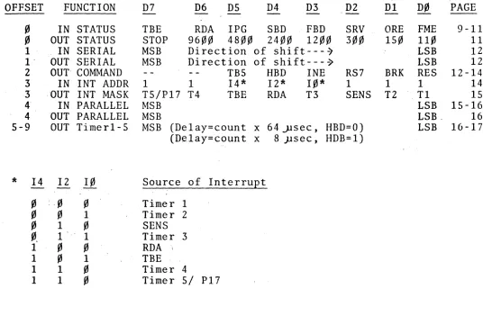
-FIGURE 2
SUMMARY OF REGISTER FORMATS FOR TU-ART, EACH DEVICE
.REF. OFFSET FUNCTION D7 D6 D5 D4 D3 D2 Dl D., PAGE
-.,
IN STATUS TBE RDA IPG SBD FBD SRV ORE FME 9-11.,
OUT STATUS STOP 96~~ 48"~ 24"~ 12.,., 3~" 15., 11., 11 1 . IN SERIAL MSB Direction of shift---~ LSB 12I' OUT SERIAL MSB Direction of shift---~ LSB 12 2 OUT' COMMAND TB5 HBD INE RS7 BRK RES 12-14 3 IN INT ADDR 1 1 14* 12* 1.,* 1 1 1 14 3 . 'OUT INT MASK TS/PI7 T4 TBE RDA T3 SENS T2 Tl 15
4 IN PARALLEL MSB LSB 15-16
4 'OUT PARALLEL MSB LSB, 16
5-9 OUT Timerl-5 MSB (Delay=count x 64 J.lsec , HBD=O) LSB 16-17 (Delay=count x 8 )lsec, HDB=I)
* 14 12
!!
Source of InterruEt.,
: ..,
.,
Timer 1.,
.,
1 Timer 2.,
1.,
SENS."
1 . , 1 Timer 31
., .,
RDA ;1
.,
1 TBE1 1
.,
Timer 41 1
.,
Timer 5/ P17 [image:26.612.40.576.156.517.2]-CONNECTING THE TU-ART TO I/O DEVICES
J2 PARALLEL A
-Signal Voltage
Pin Name Direction Level Function
I Invert Input TTL Used for normal/reverse address switching. See discussion on page 3.
2 Input Strobe A Output TTL When active indicates that the data present on input bits ~-7 is being sampled.
3 Vcc Output +5V
4 Bit 6 Input TTL
5 4 Input TTL
6 2 Input TTL
7 ~ Input TTL
8 Disable Input· TTL Turns the output drivers for the parallel output bits off.
9 Output Strobe Output TTL Indicates that data is present on parallel out-put bits ~-7.
10 Bit 6 Output TTL'
11 4 Output TTL
12 2· Output TTL
13 ~ Output TTL
14 Signal Ground Output ~V
15
5ENS A
Input TTL Interrupt request, input toIC 4 5501 (A)
16 Bit 7 Input TTL
17 5 Input TTL
18 3 Input TTL
19 1 Input TTL
20 NMI Input TTL Non maskable interrupt.
This pin is tied directly. to pin 12 of the 5-100 bus. Consult the 2-80 manual for use. Only usable with the Cromemco ZPU card.
21 Wait Input TTL This pin is tied directly. to Pin 72 (PRDY) of the S-100 bus. Stops the CPU when active.
-Signal Voltage
Pin Name Direction Level Function
22 Bit 7 . Output TTL
23 5 Output TTL
24 3 Output TTL
15 1 Output TTL
-J3 PARALLEL B Pin 1 2 3 4 5 6 7 8 9 10 11 12 13 14 15 16 17 18 19 20 21 22 23 24 25 Name Invert
Input Strobe B
Vcc Bit 6
4
2
~
Disable
Output Strobe
Bit 6
4 2
~
Signal Ground SEN5
B
Bit 7
5 3 1 Bit-7 5 3 1 Signal Direction Input Output Output Input Input Input Input Input Output Output Output Output Output Output Input Input Input Input Input" Input Input Output-Output Output Output Voltage Level TTL TTL +5V TTL TTL TTL TTL TTL TTL TTL TTL TTL TTL ~V TTL TTL TTL TTL TTL TTL TTL TTL TTL
Tft
TTL28
-Function
Used for normal/reverse address switching. See discussion on page
When active indicates that the data present on input bits ~-7 is being sampled.
Turns the output drivers for the parallel output bits off.
Indicates that data is present on parallel out-put bits ~-7.
Interrupt request, input to IC 5 5501 (B).
J4 SERIAL A Pin 1 2 3 Name
FRAME GROUND
INPUT A
OUr A
4 NC
5 NC
6 7 8: DSR SIGNAL GND CTS
9-16 NC
25. TTY OUT .A
23 TTY. OUT A
17. TTY IN A
24 TTY IN A
18-22 NC 25-26 NC
Signal Direction , Input Output Output
9
utput Output Output Inpu.t Voltage Level+12V .. +12V +12V OV +12V +12V +12V - 29.-Function
Not connected on PC board This pin should be tied to the chassis at the back panel if an RS232 terminal is being used.
RS232 data input. RS232 data output.
RS232 data set ready. Tied to +12V through 1.Sk (RS) on PC board.
RS232 signal ground
RS232 clear to send. Tied to +12V through 1.Sk (R4) on PC Board.
Data output :current loop -(current sink)
Data output current loop + (current source)
. Data input current loop~+ (current source)
J5 SERIAL B Pin 1 2 3 Name
FRAME GROUND
INPUT B
OUT B
4 NC
5 NC
6 7 8 DSR SIGNAL GND CTS
9-16 NC
25 TTY OUT
B
23 TTY OUT B·
17 TTY IN B
24 TTY IN B
18-22 NC
25~26 NC
Signal Direction Input Output Output Output Outp~t . Output Input Input Voltage Level +12V +12V +12V OV Function
Not connected on PC board. This pin should be tied to the chassis at the back panel if an RS232 terminal is being used.
RS232 data input RS232 data output
RS232 data set ready. Tied to +12V through 1.5k(R5) on PC board.
RS232 signal ground
+12V RS232 clear to send. Tied to +12V through 1.5K (R4) on PC board.
Data output current loop -(current sink)
+12V Data output current loop +
(current source)
+12V Data input current loop + (current source)
-5V Data input current loop'"-(current sink)
-TERMINAL TO TU-ART CABLE
Pin 1# Pin 1#
2 TXD 2 TXD
3 RXD 3 RXD
4 4 RTS
,
5 5 CTS
6 6 DSR
7 GND 7 GND
8 8 DCD
20
t---
15ft·---r
(length optional)
20 DTR
DB 25P DB 25P
Male Connector Male Connector
This is a diagram of the cable required to connect
a serial RS-232 I/O device (such as a CRT terminal) from the DB 25-S socket of the TU-ART cable (model TRT-CBL) to the DB 25-S connector of the RS-232 device.
-ORIGINATE MODE MODIFICATION
The TU-ART is factory wired for answer mode on both A and B serial I/O channels. This means that RS232 serial data is input to the TU-ART on J4 pin 3 (Channel A) or J5
pin 3 (Channel B), and that serial data is output from the
TU-ART on J4 pin 2 (Channel A) or J5 pin 2 (Channel B).
The TU~ART can be configured for originate mode (that
is, assume the role of terminal) by reversing the direction of data flow on pins 2 and 3 of J4 and/or J5. Pads have
been provided in the area between J4 and J5 for doing this. The modification can be made to either or both channels.
Note that there are two vertical rows of pads. Those closest to J4 are labeled A and affect Channel A only while
those closest to J5 are labeled B and affect Channel B only. The uppermost pad is connected to pin 2 of the DB-25
connector and is also connected by a short foil trace on the solder side of the board to the bottom pad. The bottom
pad is connected to a data output driver (IC
9).
The pad second from the top is connected to pin 3 of the DB-2S con~ nector and is also connected by a short foil trace on thesoler side to the pad 3rd form the top. The pad third from
the top (labeled "in") is connected to a data receiver (IC 11).
To modify the board for originate mode, proceed as follows:
(The modification is the same for both channels)
1. Cut the trace connecting the top and bottom pads on the solder side. (For Channel
A
be certain to cutthe trace between 2 pads and not the trace between
-the bottom pad and IC 9 Pin 4).
2. Cut the trace between the pad 2nd from the top and the pad 3rd from the top.
3. Connect a jumper from the bottom pad (out) to the pad 2nd from the top.
4. Connect a jumper from the "pad 3rd from the top (in)
to the top pad.
SPARE RS232 DRIVERS AND RECEIVERS.
There are two uncommitted sections in IC 9, A 75189 driver. Pads for jumper wires have been provided at pins
1, 2, 3 and at pins 11, 12, 13.
There are two uncommitted sections on IC 11, A 75188 Receiver. Pads have been provided at pins 4, 5, 6 and at
pins 8, 9, 10.
These uncommitted sections are shown on the schematic
diagram.
-~tWMEMCO COOS Z~O ASSEMBLER V. 1 .4A SAMPLE iJR00HAM. ONE-SE~ONO METROi-.JOME.
PA";E 0002
0000
0)00 1-=3
0101 310003 0104.3EOO 0106 0354 OIOd 3E09 OIOA 0302 OIOC 3ECO OIOE 0300 0110 3EOI 0112 0303
0114 3EOU 0116 D353 011 tj 3E02
o
II A ED41 .o
II ~ ED5E 01 J E CD2COI0121 ~32101
0124 05 0125 C22t:01 .0128 3E07
Ul2A D301
012C 0610 012f 3E70 013U 0305
0132 fB 0133 C9
0134
0200 2401
0002 ; 0003 ; 0004 ; 0005 ; 0006 ; 0007 ; 0008 ; 0009 ; 0010 0011 ; 0012 0013 0014 0015 0016 0017 0018 0019 0020 0021 0022 ; 0023 0024 0025 0026 0027 002d ; 0029 0030 ;
RINGS THE CONSOLE BELL AT I-SECOND INTERVALS. SET SrlITCHES 1, 7, AND 9 OFF, ALL OTHER
SvdTCHES ON THE TUART DIP Sr'd rCH ON. SET CONSOLE TEHMINAL BAUD RATE TO 9600. CONNECT TERMINAL TO rUART CONNECTOR J4,
(SERIAL A).
ORG 01 LD LD OUT LD OUT LD OUT LD OUT LD OUT LD LD 1M2 CALL ) OOH SP",300d A,O 54H,A A,9 2,A A,OCOH O,A A, I 3,A A,O 53H,A A,2 I,A I NIT
;SELECT DEVICE A (SEE ; SOFTWARE ADDR-Rt: VERSE) • ;RESET DEVICE A
&
ENABLE ; INTERRUPT ACj(. RESPONSE. ; SET BAUD RATE;TO 9600.
;MASK OUT ALL INTERRUPTS ;BUT THOSE FROM TIMERI, ;DEVICE A.
;MASK OUT ALL INTERRUPTS IFROM DEVICE B.
;SELECT PAGE 2
II-=OR INTERRUPT VECTORS. ; I NTE RRUPT MODE 2.
IINITIALIZE THE TIMER.
0031 ; WrlAT FOLLOWS IS AN H~FINITE LOOP. IT COULD 0032 INSTEAD BE SOME USEFJL PROGRAM ENTIRELY UN-0033 ; RELATED TO THE TIMER PROGRAM.
0034·· ; 0035 HERE: 0036 ; 0037 ;
JP rifRE
0038 ; INTERRUPT SERVICE ROUTINE. 0039 ;
0040 TIMER: 0041
0042 0043 0044 :; 0045 INIT:
0046 TM2:
0047 0048 0049 {)U50 ;
0051 ;
DEC JP LO OUT LD LO OUT EI RET B' NZ, TM2 A,7 J ,A B,125 A,125 5,A
- ;OUTPUTTING 7 TO ;THE CONSOLE ~ILL iRINU THE BELL. ;MULTIPLIER FACTOR. ;COUNT fOR TIMERI
;(125
*
64 USEC = 8 MSEC) •.. 0052. 0053
OR0
-uw
200H. TIMER ; INTERRUPT VECTOR, TIMERI.ANNOTATED SOFTWARE EXAMPLE
-TU-ART KIT ASSEMBLY INFORMATION
If you purchased your TU-ART as a kit you will find the
assembly to be straightforward. The locations of all the
components are clearly marked on the pc board itself.
Take care that the parts are positioned and oriented
properly before they are soldered in place.
When installing the IC sockets note that no socket should
be installed in the position marked "status socket". A
socket is only used here if there is a need to change the
assignment of status bits in the status word, as described
on pages 6 and 7 of this manual.
Also note that three different three-terminal regulators
are used in the TU-ART: a 7805, 7812, and 7905. These
regulators are not interchangeable. Take caution that
each regulator is installed only in the proper position.
It is important that the "+" end of the tantalum capacitors
are oriented as marked on the pc board. The cathode
(banded) end of the IN4742 diode (01) must be oriented
to the left. The flat surfaces of transistor QI and Q2
should also face the left.
After soldering all parts in place, install the ICs in
their sockets. BE,VERY CAREFUL THAT EACH PIN OF EVERY IC
IS PROPERLY ENGAGED IN ITS SOCKET. After installing the
ICs carefully inspect your work.
TU-ART PARTS LIST
Integrated Circuits Capacitors
IC 1 7442 C1 0.1 uF
IC 2 74367 C2 .05 uF
IC 3 74368 C3 0.1 uF
IC 4 5501 C4 0.1 uF
IC 5 5501 C5 .05 uF
IC 6 74367 C6 10· uF
IC 7 74368 C7 0.1 uF
IC 8 74LSll C8 0.1 uF
IC 9 75189 . C9 10 uF
IC 10 7406 C10 0.1 uF
IC 11 75188 C11 0.1 uF
IC 12 74LS74 C12 10 uF
IC 13 74LS08 C13 0.1 uF
IC 14 74367 C14 0.1 uF
IC 15 74368 C15 0.1 uF
IC 16 74367 C16 0.1 uF
IC i7 74368 C17 0.1 uF
IC 18 74367 C18 75 pF
IC 19 74367 C19 75 pF
IC 20 74367 C20 10 uF
IC 21 74367 C21 .05 uF
IC 22 74LS32 ·C22 10 uF
IC 23 74LS08 C23 30 pF
IC 24 74LSll C24 0.1 uF
IC 25 74LS74 C25 0.1 uF
IC 26 7805 C26 0.1 uF
IC 27 7812 C27 0.1 uF
IC 28 74900 C28 10 uF
IC 29 74L04 C29 10 uF
IC 30 74367 C30 0.1 uF
IC 31 74367 C31 O.luF
IC 32 74367 C32 300 pF
IC 33 74367 IC 34 74LSOO IC 35 74LS157
Diodes/Transistors IC 36 74LS04
IC 37 7905 01 1N4742 Zener
IC 38 7406 Q1 2N3906
IC 39 74LS04 02 2N3906
IC 40 74LS04 IC 41 74LS74 IC 42 74LSOO IC 43 74LS03 IC 44 74373 IC 45 74L04 IC 46 74LS136 IC 47 74LS136 IC 48 74LS74
-Resistors
Rl lK R2 390 R3 470 R4 1.5K R5 1.SK R6 680 R7 18K R8 18K R9 470 RIO 1.5K Rll 1.5K R12 680 R13 390 R14 lK R15 lK R16 330 R17 330 R18 47 iU9 47 R20 220 R2l lK R22 lK R23 lK R24 lK
RNl 4.7K DIP RN2 4.7K DIP
TU-ART PARTS LIST (Cont.)
(15 resistors) (15 resistors)
38
-IC Sockets
2 40 pin sockets 1 20 pin socket 23 14 pin sockets 21 16 pin sockets
Miscellaneous
Printed circuit board 10 pole DIP switch 4 26-pin cable sockets 1 Heatsink
5 6-32 screws 5 6-32 nuts 8 2-56 screws 8 2-56 nuts
~
•
•
...
MADE IN USA
J2 PARALLEl A
-
-.
n.w ~
•
Co> 0-• C3L---J-3--PA-R-A-ll-E-L--a---J C2 em:::> CD ~;
•9
nA
•
n CIt .... ~ '" '"...
oo
...
<
B
--
n....
0-~
•
Co>
0-....
--
n 'of n --'of -~ Co>0-•
1~
-
n ~ ~•
,.. '"~9
24 C13-
n w o ~ Co> 0-~J4 SERIAL A FME "'''' ORE g;: SRV "' .... FaD :::;;
SBO IPG ROA TBE o 1 2 3 4 S 6 7 C::=>C7 n
---0 ~...
Co> 0-~-
n
~ o ~...
Co> 0-~ C14-...
... '" Co> ~ Co>TU-ART PARTS PLACEMENT DIAGRAM
n
~
...
•
-
n
w w ~ Co> 0-~ C25 "-~•
,.. o•
-
• z-ARROWS MARK PIN 1
TU-ART
LEGEND
•
o
TU-ARI' THEORY OF OPERATICN
I. INTRODUCTION
The TU-ART has ten functional blocks supporting the TMS 5501s:
A. Power Supply Three IC regulators and a zener diode are used to
generate ±5 and ±12 volts.
..
B. Crystal Controlled Clock An 8 MHz crystal oscillator is used as
an on-board reference to control the internal state machine and
to drive the 01 and 02 clocks of the TMS 550ls.
C. Address Select Two four-bit address comparators generate base
address select signals when the four most significant device
address bits of an input or output instruction agree with one of
the two base address switch settings on the TU-ART. The base
address select signals enable the appropriate TMS 5501 (depending
on the current state of the Address Reverse multiplexer).
D. Function Decode The four function address pins on the TMS 5501s
are driven by a read only memory addressed by the lower four bits
of the S-IOO address bus and status signal WOo The ROM also generates signals for internal bus control.
E. State Sequencer The internal state sequencer starts up whenever
the TU-ART is addressed and cycles the internal bus. through an
8080 M3-like sequence. The sequence starts with a SYNC pulse to
the 5501s while the internal data bus is strobed with status
informa-tion appropriate to the type of cycle requested by the processor
(Io read, 10 write, or Interrupt Acknowledge); contiriueswhile
data is written or read; arid terminates after signalling READY to
the processor.
F. Status Strobe Data bus pins D0 and Dl are controlled by the
status strobe circuit during internal SYNC time to select the
proper TMS 5501 operation.
G. Bus Multiplexers The internal data bus is time multiplexed (for
status information); direction multiplexed (depending on the type
of cycle: read or write), and pqth multiplexed (depending on theparticu~
lar read-type function being performed) under control of the state
generator and three-state bus drivers.
H. Serial Interface The TTL level serial output signal from the
TMS 5501s is converted to EIA RS/232 levels and to a teletype
compatible current switch. Serial input may be from either EIA
or teletype.
I. Parallel Interface TTL Bus buffers drive the parallel ports.
Handshaking signals are controlled by the function decoder ROM.
J. Priority Chain A ripple priority resolver controls Data bit D0
(INTA) on each TMS 5501 during SYNC time. This prevents both
devices from responding to an Interrupt Acknowledge cycle from the
processor when both devices have active interrupt requests. The
priority chain is expandable to multiple boards.
These ten blocks, which are listed in the approximate order of
attack for troubleshooting, will be discussed in detail below.
II. Power Supply
The TMS 5501s require three power supplies: VCC
=
+5, VDD=
+12,and VBB
=
-5. A -12V source is created by zener diode Dl for the EIAline driver and receiver IC's. The +12 supply is used by the EIA line
drivers, the TTY interface, and the 01, 02 clock drivers. The-5
supply is used by the TTY interface.
III. Crystal Controlled Clock
An 8.000 MHz crystal oscillator generates the TU-ART's timebase.
A two-phase, 2MHz clock is derived from 1('4lP8 (02TTL) and 1042P6
(01TTL). These signals are followed by high voltage inverters to
generate the 12 volt clocks for the TMS 5501s. Transistors Ql and Q2
form edge-active pullups for the inverters. A 75 pf - 330 ohm
differentiator network on the base of each transistor couples a
spike from the falling edge of the TTL input into the base. This
switches the transistor on briefly and pulls the collector to +12
volts. A 47 ohm series resistor in the clock lead reduces ringing
and overshoot. The rising edge of the TTL input turns on the 7406
inverter which pulls the collector of the transistor (now off) back
to ground.
The state generator is clocked by 02TTL and 02TTL outputs from
IC4lP9 and IC41P8.
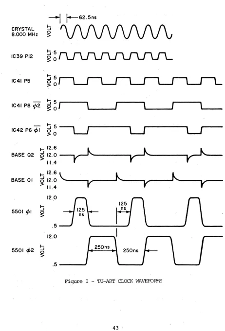
Clock waveforms are summarized in Figure I.
IV. Address Select
Four-bit address comparison is performed by open collector exclusive
or gates IC46 and IC47. Incoming address lines are deglitched and
inverted by 74L04 inverters, then ex-ored with 4 bits from the DIP
swit~h base address select positions. A closed switch matches a "1"
on the address bus; an open switch matches a "0" on the Address bus;
when all four bits match and SOUT or SINP is active then th~ open
collector wired - and node will go high. If the node at RN2r7 is high
Base Address B is being selected. If RN2P5 is high Base Address A is
being selected. When Device A is addressed IC43P6 pulls down the
Device B select node to prevent bus conflict if both base addresses
accidentally have been set equal. When either Device select is active
~
r-S2.5nSCRYSTAL ~
8.000 MHz 0 >
IC39 PI2 ~·5 ~O
~5
IC41 P5 ~O
IC41 P8 cj>2 ~5
~
0
1
\
I
\
I
\
~5
IC42 PS ~I
~O
~ 12.S
~ ~
BASE 02 ~ J 12.0 11.4
BASE 01
~ 12.S \..
~
k.
012.0
V
V"
V'
:> 11.412.0
~ 125
5501 cj>1 ns
~
.5 12.0
5501 ~2 0 ~
>
.5
Figure I - TU-ART CLCCK t'lAVEFOR-1S
[image:44.612.85.547.75.756.2]IC40PlO goes low, enabling the Function Decoder ROM. Multiplexer IC3S
performs Base Address reversing when its select pin goes low. In the
normal case Device A select enables the CE driver of IC4, while Device
B select enables the CE driver of ICS. Base address reversing enables
IC5 in IC4's place and vice versa. The select pin of the MUX, IC35Pl
is controlled by the signal applied to J2Pl or J3Pl; or, if DIP Switch
2 is closed, by IC4P31 (the MSB of Device A's output parallel port).
v.
function DecodeTTL PROM IC28 is enabled when IC28P15 goes low (which occurs at
the beginning of Input and Output cycles). IC28 is not enabled during
interrupt acknowledge. When IC28 is enabled, it supplies function
address signals to the 4 address pins of the S501s., IC28P5 goes low
during I/O operations involving the parallel ports and drives ICl, a
decoder chip which generates Input and Output strobe signals. IC28P6
goes low during Output_cycles. This signal controls the incoming bus
buffers, generates a state-cycle request by pul~ing down IC24PIO, and
is strobed on the internal data bus bit Dl at SYNC time by I~43P3.
IC28P7 goes low during INPUT cycles. rhis signal controls the outgoing
bus drivers and generates a state-cycle r~quest by, pulling down IC24P9.
This signal is not active (floats) during INTA cycles. I28P9 goes low
when the status port of the TMS 5501s is read. This signal ,controls
an internal data path from the TMS 5501s to the output,data latch, IC44.
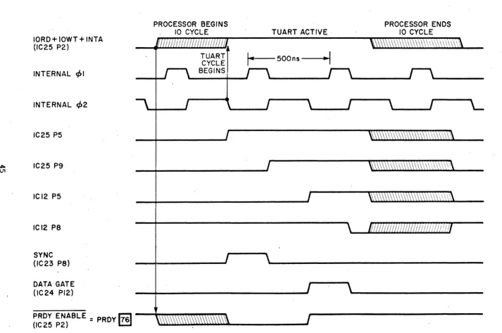
VI. State Sequencer
The heart of the TU-ART is the state sequencer, a four-stage shift
. .
register which times the status drivers and data in/out circuits to
form an 8080-like internal bus. The input to the state sequencer,
IC25P 2, is the signal from IC36P6( I 0 READ + IOWRITE + INTERRUPT
ACKNOWLEDGE). While this signal is low, the state sequencer is held
IORD+l0WT+INTA (IC25 P2)
INTERNAL q,1
INTERNAL q,2
IC25 P5
"" IC25 P9 (".'1
ICI2 P5
ICI2 P8
SYNC (lC23 P8)
DATA GATE (IC24 P12)
PRDY ENABLE
=
PRDY1761
(IC25 P2)
PROCESSOR BEGINS 10 CYCLE
TUART CYCLE BEGINS
TUART ACTIVE·
I
...
t - - -500 ns - - - - I .. ~IFigure II - TU-ARl' STATE ~ TIMING
[image:46.792.41.754.76.549.2]in a reset state by direct clear pins 1 and 13 of ICs 25 and 12.
When the input goes high a high level will be shifted to IC25P5 at the
first falling edge of 02. IC23P8 then goes high, generating a SYNC
signal at Pin 19 of both TMS 550ls and turning on status strobe
driver IC18 through IC40P6 and IC43Pl.
The state sequencer is now clocked by the rising edge of 02,
shifting a high level to IC25P9. IC23PIO goes low and remains low
until the state sequencer is reset at the end of the I/O cycle. The
status strobe drivers are shut off. The TMS 5501 now arranges internal
data paths according to the address and status information it received
during SYNC time. If the TU-ART is in an rOWRITE cycle the S~lOO DO
bus receivers IC18 and IC30 are enabled.
The state sequencer is clocked for a third time by 02 falling edge,
propagating the high level at rC25P9 to IC12P5. The Gate input of the
DI bus latch is raised (IC44Pll). ThePRDY driver IC16 is disabled,
signalling "READY" to the CPU, and releasing the bus from its WAIT
condition.
The final change in state occurs on the rising edge of 02 when
IC12P8 goes low. This shuts off the DI latch gate. The state sequencer
has completed its cycle and remains in this state until the processor
terminates the I/O cycle.
VII. Status strobe
The TMS550ls have no control pins for DBIN or WR; instead the lCs
monitor bits D0 and Dl of the data bus during SYNC for status
informa-tion. If D0 is high during SYNC, an futerrupt Acknowledge cycle is
beginning, and the 5501 will send data to the bus during !lT3" of the
cycle. If Dl is high an IOREAD operation is beginning and the 5501
'whose CE pin was high during SYNC will access the internal register
addressed by A3-A0 and present data to the bus at "T3" of the cycle.
If Dl is low during SYNC, an IOWRITE operation is beginning and the
5501 whose CE pin was high during SYNC will latch data from the bus
during "T3" of the cycle.
Bit Dl is controlled by an open collector nand, IC 43.which is
strobed by SYNC. Bit D0 is split ir.to D0A and D0B so that INTA can
be'sent to the TMS 5501s individually. This is necessary because
CE no longer selects the chip during interrupt acknowledge.
.Three-state driver IClS controls D0A and D0B during SYNC.
VIII. Bus Multiplexers
The internal data bus which connects the two TMS 5501s will float
while idle. At. the beginning of a cycle it is strobed by the status
drivers as described in section VII. Following status the bus assumes
one of five configurations:
A. IOWRITE cycle: The S-lOO DO bus receivers drive the internal
data bus during WR • (T > T2).
B. rOREAD (EXCEPT READ STATUS PORT): The internal data bus is
buffered by a set of permanently-enabled 74367 sections, then passed
through another set of 74367s, enabled by the assertion of READ and
STATUS. These 74367s drive the output latch IC44 which latches during
,T3 of the internal cycle. IC44 has three state output drivers built
in which drive the S-100 DI pus during DBIN • IOACTIVITY.
C. IOREAD STATUS: The buffered internal data bus passes through
the status bit select pocket where bits from the 5501 may be arranged
arbitrarily in order to control flag bit assignments. The "scrambled"
bits are then passed through 74367s.which have been enabled by STATUS
going low. The output latch operates as before.
D. INTA Mode 2 (Z-80): During a mode 2 INTA the buffered
internal data bus bibs D3-D5 plus INTA B plus A7 A6 and A5 from Base
address A form inputs to a set of 74367s which drive the output latch.
E. INTA MODE 0 (8080): During MODE 0 INTA the buffered internal data bus bits D3-D5 are routed through 74367s straight to the output
latch. The remaining bits are passively pulled high.
IX. Serial Interface
Transmit output from the TMS 5501 is inverted to RS232 levels by
Iell (1488). Output is also provided from a 7406 high voltage inverter
for grounding a 20 rnA current source or for TTL level output. The
RS232 output idles at -12v, the 7406 output idles at ground (conducting).
Receiver input is taken from an RS 232 line receiver, Ie9 '(1489).
Ie9 converts RS232 levels to TTL. When a TTY keyboard is used, it
switches the bias voltage on leg from +12 to -5 which causes TTL
level switching at the output.
The output of the 1489 idles at +5 volts.
X. Parallel Interface
Parallel inputs to the TMS 5501 are TTL buffered by 74367s.
Paral-lel outputs are inverted and buffered by 74368s to keep positive
logic. The 74368s may be three stated by grounding DISABLE. Strobe
signals are decoded by Iel.
XI. Priority Chain
The TU-ART will respond to an Interrupt Acknowledge cycle from the
processor when three conditions are satisfied: 1) The processor has
raised SINTA, the Interrupt Acknowledge status signal 2) One of the '
TMS 5501s is requesting interrupt (high level on IC4P23 or IC5P23) and
3) No other device higher up the prio~ity chain is requesting an
inter-rupt. The priority chain input at Jl is used to clear IC48, the INTA
enable flip flop. Suppose IC4 (Device A) requested an interrupt at the
same time as IC5 (Device B). If Priority IN was bein~ held low by a
hi~her Drioritv TU-ART, both sections of IC48 would remain cleared,
disabling IC23P5 and IC23P6 from generating SINTA status bits. When
Priority IN is allowed to float to +5, the next Ml occurrence will clock
the two sections of IC48 (Ml may be the start of an INTA cycle, though
it doesn't have to be). Both IC48P5 and IC48P9 go high momentarily
because both DEVICE A and Device B have interrupts pending. However
IC48P6 ripples through IC13P3 to force IC48P9 low in exactly the same
manner as PRIORITY IN from Jl. Thus only DEVICE A actually receives the
INTA status bit and no bus conflict is allowed'.
WARRANTY
Your factory-built TU-ART is warranted against defects in materials and workmanship for a period of 90 days from the day of delivery. We will repair or replace products that prove to be defective during the warranty period provided that they are returned to Cromemco. No other warranty is expressed or implied. We are not
liable for consequential damages.
Should your factory-built TU-ART fail after the warranty period i t will be repaired, provided
that i t is returned to Cromemco, for a fixed service fee. We reserve the right to refuse to repair any product that in our opinion has been subject to abnormal electrical or mechanical abuse. The service fee is currently $35 and is subject to change.
Your assembled TU-ART kit will be repaired, provided that i t is returned to Cromemco, for a fixed service fee,;~e reserve the right to-refuse to repair any -kit that in our opinion has not been assembled in a workmanlike manner or has been subject to abnormal electrical or mechanical abuse. Payment of the service fee must accompany the returned merchandise. The service fee is currently $35 and is subject to change.
.l============================
-l---+-+--++--'~
I
t---::::::.d---t--t---1(~==----t-~
II i
I I!
f , I
Ii
I
'
I
In-
I-I
I :I I I
I I j I
I!
!! I
II
i
I
I:~---~"-~~
I 11
!
' I ! :
I ! I i
II
I
L -_ _ _ _ _ _ _ _ _ _ _ _ _ _ _ _ _ _ _ _ _ _ _ _ _ _ _ _ _ _ _ _ _ _ _ _ _ _ _ _ _ _ _ _ _ _
D£.\'>C£ "
ADt'P.~SS
shier
I'---<J]~
I"---<!il:
~
P!--f-J.C;~L---<Jl. ~
~l
~---<Dcu
SfHSf!''--' --"'-oQ.lf!+--,,<"
m
-,,,,
Dt:Y!:;c[ A
--H++--Oj' "
.
.,;"\
---H+t-'l'"
~
"I::....
\)w-,~rr·
1489
SEO,,, ..
COPYRIGHT 1977 BY CROMEMCO
SCHEMATiC REV. I
BOARD REV_ B
~13' 23 II
t'lL5Oe
,
~
r"
~;Myl
.1 ru-~
1~5 +0
""lJ;-- -.l±CII I '<1,1,8,10,11,15-1', 1'lOliof T2"-l1,30,31
". +11"1"
---r---r-r-... ·" 01 ,""",C20 ell
IN4H2 110,..f I0051"F'
",
-UK I3
'"
'1,1~ II
'"
~
",
~
..
IoISIt Al~
, , .,
A'~O
'.
.
SINP~9
'"
~ 10 t'lLSI3S 8 7"1_1K
1_ r"V"
,n'',.)'-Iv
T+D
~
"L-..
U~~iiD
stCTlON
COPYRIGHT 1977 BY CROMEMCO
SCHEMATIC REV. 2
BOARD REV. C