DITIDISC
INCORPORATED
Display Division
Section 1
Summary Specifications
DISC SPEED
DATA RATE
DATA CAPACITY
1800 RPM +1. 3% -3%
Hysteresis-Synchronous Motor
3.0 Mbps per track
100, 000 bits per track
(Tracks can be added in incre-ments of 8, up to 64. )
INPUT/OUTPUT LEVELS
TEMPERATURE
Operating
Non-Operating
ATMOSPHERE
o
and +5VTTL integrated-circuit interface (+5V Power Supply TI Series 74)50°F to 105°F; less than 200F change per hour
-200F to +1300F
Corrosive atmospheres such as those found in steel and chemical plants are not permitted.
VIBRATION
Floor vibration of O. 15 g's max. from 10 to 65 Hz. The disc package shall not be damaged by 5 g's or less of shock in any axis.
A-C POWER
SIZE & WEIGHT
120 volts -t 10%, 60 ~: ~HZ, single phase, 8.2 amperes starting (10 sec. ); 2.6 amperes running
Section 2
General Description
2. 1 ELECTRICAL
The FPD-Series ,Fixed-Head garallel-~igital
Disc Memery System has a 12-inch disc which can contain as many as 64 data tracks with up to 100, 000 bits on each track. This disc ro-tates at 1, 800 RPM to provide a maximum bit rate of 3-million bits per second.
The FPD unit is designed for buffer-storage applications. Because the F PD unit uses synchronous clocking from a clock track, it is recommended only for buffer storage ap-plications. The time stability between tracks cannot be guaranteed for long periods of time. Where Data is to be stored for an indefinite period, the DATA DISC F6 Disc Memory System should be employed.
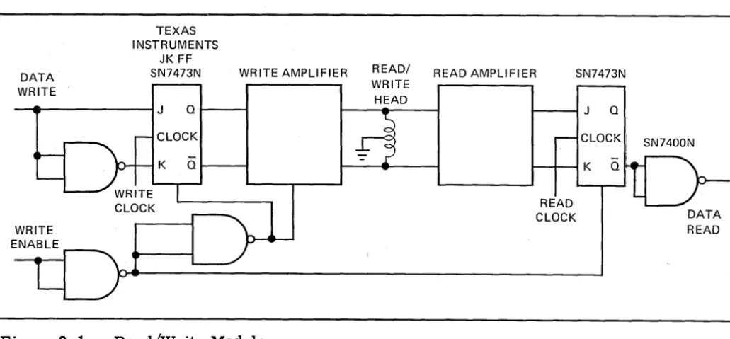
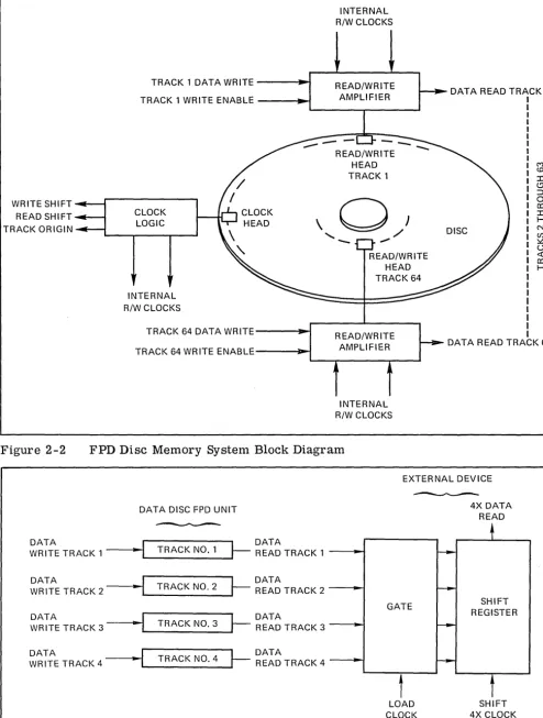
Each track is complete with a read/write head and all electronics to perform the following functions, as diagrammed in Figures 2-1 and
2-2:
Encode Data Write Data Read Data
Decode Data Re-Clock Data
Any number of tracks may be written or read in parallel because each has a clocked flip-flop output. The standard write -amplifier
DATA WRITE
TEXAS INSTRUMENTS
JK FF
SN7473N WRITE AMPLIFIER
---~ J Q t - - - - t
WRITE
ENABLE r - - - _
Figure 2-1
CLOCK
K Q t - - - - t
Read/Write Module
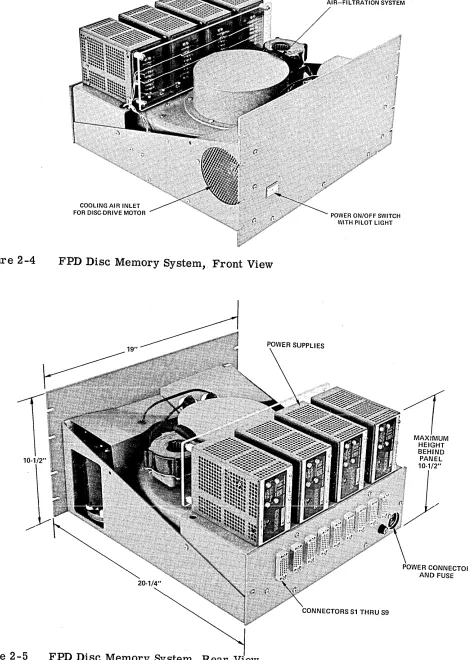
power supply will accommodate 10 write am-plifiers in parallel. Larger supplies can be provided where it is necessary to write on more than 10 tracks simultaneously. Power and input/output connectors are on the rear of the unit, Figure 2-5.
2. 2 MECHANICAL
The cast-aluminum disc-module chassis is shock-mounted within the rackmount tray. The chassis includes the heads, 12-inch disc and read/write electronics.
FPD Series units are 10-1/2 inches high and 19-3/4 inches deep (not including space for cable breakout) and are designed for mounting into standard 19-inch-wide racks or rack cabinets. Power supplies are mounted at the back of the rackmount tray. See Figure 2-5.
2.3 SYSTEM APPLICATION
The FPD unit is designed so that each track on the disc is a complete channel. A high-speed processor can access each track and update the data stored on any track. Where data rates higher than 3-million bits per sec-ond are needed, several tracks can be com-bined to form the data buffer. For example, data read from four channels may be loaded into a four-bit shift register and a 4X clock used to shift the data into the output channel at a 12-million-bit rate. Other bit rates may be achieved by using similar combining
techniques. See Figure 2-3.
READ/ WRITE HEAD
READ AMPLIFIER SN7473N
t---~ J Q
CLOCK I i
t---+-~ K
READ
CLOCK
SN7400N
[image:3.620.36.552.495.734.2]WRITE SHIFT READ SHIFT TRACK ORIGIN
TRACK 1 DATA WRITE ---~
TRACK 1 WRITE ENABLE ---~
CLOCK LOGIC
INTERNAL R/W CLOCKS
TRACK 64 DATA WRITE---~
TRACK 64 WRITE ENABLE---~
INTERNAL R/W CLOCKS
READ/WRITE HEAD TRACK 64
READ/WRITE AMPLIFIER
INTERNAL R/W CLOCKS
DATA READ TRACK 1
M
(0
:::c
(!) ~
o
a:
:::c
l-N
CJ)
~ u
<t:
a:
I-DATA READ TRA K 64
Figure 2-2 FPD Disc Memory System Block Diagram
EXTERNAL DEVICE
---DATA DISC FPD UNIT 4X DATA
READ
. - - - .
~
DATA
·1
DATAWRITE TRACK 1 TRACK NO.1 ~ READ TRACK 1
--·1
DATA
TRACK NO.2 ~DATA
WRITE TRACK 2 READ TRACK 2 ~
GATE SHIFT
DATA
·1
~DATA REGISTERWRITE TRACK 3 TRACK NO.3 READ TRACK 3
-
~DATA
·1
TRACK NO.4 ~DATAWRITE TRACK 4 READ TRACK 4 I..-.-.
t
t
LOAD SHIFT
CLOCK 4X CLOCK
[image:4.623.74.569.58.711.2]Figure 2-4
Figure 2-5
COOLING AIR INLET FOR DISC-DRIVE MOTOR
FPD Disc Memory System, Front View
FPD Disc Memory System, Rear View
AIR-FILTRATION SYSTEM
POWER ON/OFF SWITCH WITH PI LOT LIGHT
CONNECTORSS1THRUS9
~
MAXIMUM HEIGHTBEHIND PANEL 10-1/2"
I /
/
Section 3
Input/Output Details
3.1 INPUT/OUTPUT LINES
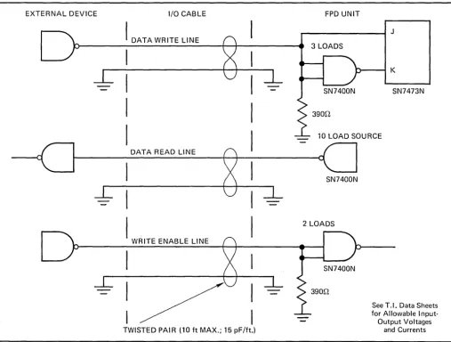
Each track has three input/output lines that connect to the external device via an I/O Cable as described in Figure 3-1. The FPD unit use s Texas Instruments Series SN7400N and SN7 47 3N TTL Integrated Circuits.
3. 2 INPUT CONNECTORS
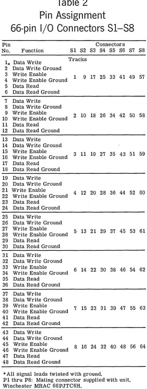
Eight 66-pin connectors are provided, each serving eight heads. The use of 16 heads requires two connectors, etc. All eight con-nectors (S1 through S8) are required when 64 heads are used. See Table 2 which also indicates the function served by each pin on each connector, and the tracks served by each.
EXTERNAL DEVICE I/O CABLE
I
DATA WRITE LINEI
I
DATA READ LINE
WRITE ENABLE LINE
3.3 CLOCKS
Five clocks, all derived from one clock track, are available in the standard FPD system. Two are used internally, and the other three are for use at the interface. The three inter-face clocks are the Track Origin (once per revolution), Write Shift and Read Shift (Figure 3-2 and Table 3).
The Write Shift Clocks are used to change the state of the Data Write line and are counted down to indicate angular position of the disc.
The Track Origin clock is derived from the four-bit gap in the clock track and is used to indicate the zero-degree position of the disc and as a reset for any counters used to iden-tify other angular positions.
A second clock track can be provided as an option.
FPD UNIT
~ __________ ~ J
3 LOADS
_ _ _ ---I K
SN7473N
10 LOAD SOU RCE
SN7400N
2 LOADS
TWISTED PAIR (10 ft MAX.; 15 pF/ft.)
See T.I. Data Sheets for Allowable Input-Output Voltages
and Currents
[image:6.620.60.567.342.726.2]FPD units are supplied with factory-written clocks. However, if new clocks are to be written, the Clock Write Enable lines can be accessed as detailed in Table 4.
3.4 CLOCK CONNECTOR S9
S9 is a 66-pin used only by the clock tracks. See Table 4 for pin assignments.
Table 1
, Data Input/Output Lines
Data Write 1 thru 64:
An input line that is driven from the output of an exter-nal flip-flop that is clocked by Data Write Shift Clock. Write Enable 1 thru 64:
The Write Enable line going high will cause the data on the corresponding Data Write line to be written on the track. As long as the Write Enable line is high, writ-ing will continue.
Data Read 1 thru 64:
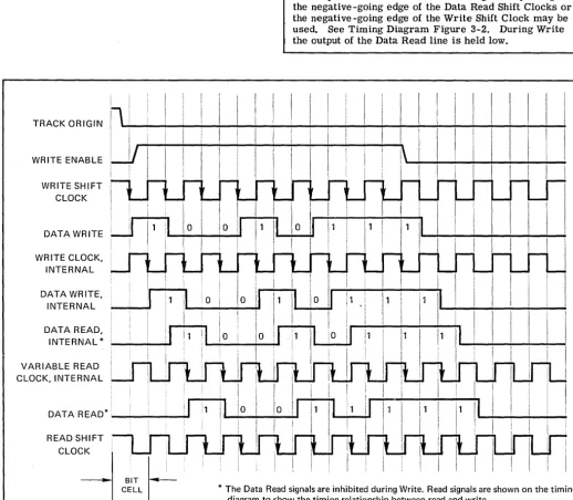
Each Data Read line is the buffered output of a clocked flip-flop. The Data Read is delayed from Data Write and may be shifted into an external register by using the negative-going edge of the Data Read Shift Clocks or the negative-going edge of the Write Shift Clock may be used. See Timing Diagram Figure 3-2. During Write the output of the Data Read line is held low.
TRACK OR IG IN
Il _______
~---...---...~-;-...-.;-I---I
____
II
II.---"!WRITE ENABLE
WRITE SHIFT CLOCK DATA WRITE WRITE CLOCK, INTERNAL DATA WRITE, INTERNAL DATA READ, INTERNAL *
VARIABLE READ CLOCK, INTERNAL
j
I
!II I i
I
I I 1DATAREAD* __________ _
READ SHIFT
Figure 3-2 Timing Diagram
0
II
I.
I I
i
I
I
il
i
10
I'
II
I
I
\0
10
II
i
II
I
II
I1
I
I
10
I
I'
II
I
:1 , I '1
I
I
I II
I
I
I
i I I
I
II
0 ! 1 11II
I I
i
I
I
I
I
l
I
i'1
l~'
I
I
I .
[image:7.621.38.556.262.713.2]Table 2
Pin Assignment
66-pin I/O Connectors
Sl-S8
Pin Connectors
No. Function S1 S2 S3 S4 S5 S6 S7 S8
1* Data Write Tracks
2 Data Write Ground 3 Write Enable
4 Write Enable Ground 1 9 17 25 33 41 49 57 5 Data Read
6 Data Read Ground
r"7 Data Write I
8 Data Write Ground 9 Write Enable
10 Write Enable Ground 2 10 18 26 34 42 50 58 11 Data Read
12 Data Read Ground
13 Data Write
14 Data Write Ground 15 Write Enable
16 Write Enable Ground 3 11 19 27 35 43 51 59 17 Data Read
18 Data Read Ground
19 Data Write
20 Data Write Ground 21 Write Enable
22 Write Enable Ground 4 12 20 28 36 44 52 60 23 Data Read
24 Data Read Ground
25 Data Write
26 Data Write Ground 27 Write Enable
28 Write Enable Ground 5 13 21 29 37 45 53 61 29 Data Read
30 Data Read Ground
31 Data Write
32 Data Write Ground 33 Write Enable
34 Write Enable Ground 6 14 22 30 38 46 54 62 35 Data Read
36 Data Read Ground
37 Data Write
38 Data Write Ground 39 Write Enable
40 Write Enable Ground 7 15 23 31 39 47 55 63 41 Data Read
42 Data Read Gr ound
43 Data Write
44 Data Write Ground 45 Write Enable
46 Write Enable Ground 8 16 24 32 40 48 56 64 47 Data Read
48 Data Read Ground
* All signal leads twisted with ground.
P1 thru P8: Mating connector supplied with unit. Winchester MRAC 66PJTC6H.
Each connector serves eight tracks.
Table 3
Clock Output Lines
Data Write Shift Clock:
A 3-million bit per second clock with 4 clocks missing at Track Origin time. The negative-going edge is used for changing state of Data Write lines.
Data Read Shift Clock:
The negative-going edge is used for sampling the center of Data Read. The center of Data Read is delayed 2 bit times from the leading edge of Data Write. The sample caused by Data Read Shift Clocks will be delayed ap-proximately two bit times relative to Data Write.
Track Origin Clock:
A once-per-revolution clock used to reset counters, etc.
Clock No. 1 Write Line:
A data input line for writing clocks. This line should be grounded except when writing a clock track.
Clock No. 1 Write Enable Line:
Taking this line positive will enable writing in the clock track. No connections should be made to this line ex-cept when writing clocks. See note on Table 4.
Clock No. 2 Read Line (option):
The output of the second clock track read amp.
Clock No. 2 Write Line (option):
A data input line for writing clocks. This line should be grounded except when writing a clock track.
Clock No. 2 Write Enable (option):
[image:8.617.58.307.51.706.2]Table 4
Pin Assignment
66-pin Clock Connector S9
*
Pin No.
1 ** 2 3 4 5 6 7 8 9 ***
10 11 12 13 14 15 16
17 ***
18
19 - 66
Function
Write Shift Clock Ground
Read Shift Clock Ground
Track Origin Clock Ground
Clock # 1 Write Line Ground
Clock # 1 Write Enable Line Ground
Disc Ready Ground
Clock #2 Read Line (option) Ground
Clock #2 Write Line (option) Ground
Clock #2 Write Enable (option) Ground
Unassigned
*Supplied with mating connector, Winchester MRAC 66PJTC6H.
** All Signal leads twisted with ground.
***These pins (9 and 17) are not inserted into the connector block. Connector S9 must be pulled away from the'rear panel to gain access to these pins for writing clocks.
Section 4
Operation
4.1 WRITE
To write, the first bit of data is placed on the Data Write line and at the correct angular position the Write Enable line is raised and writing begins. Each negative-going transi-tion of the Write Shift clock is used by the external device to transfer another data bit onto the Data Write line. The turn on of the Write Enable should occur at no later than
100 nanoseconds from the negative-going edge of a Write Shift clock.
Write Enable should be turned off at the next positive-going clock transition following the last shift clock as shown in the timing diagram, Figure 3-2.
4.2 READ
During Write the Data Read line is held low but at all other times, any data on the track will be clocked out to the Data Read line.
The data may be transferred from the Data Read line to an external device at the negative-going edge of the Read Shift Clock.
[image:9.621.75.564.454.709.2]DATA DISC
INCORPORATED
1275 CALIFORNIA AVENUE PALO ALTO. CALlFOR~IA 94304 TELEPHONE 415 326·7602
Display Division
PRICE SCHEDULE
F-SERIES PARALLEL DIGITAL
DISC MEMORY SYSTEM (FPD)
PRODUCT DESCRIPTION
Unit ccnsists of mechanical assembly (including disc), heads
(one per track or channel) with read-write-clocking module,
standard clock channel, and power supply.
The number of
channels required will dictate the model number ordered.
Channels are added in increments of eight.
PRICING:
FPD-8
FPD16
FPD24
FPD32
FPD40
-Unit
$
7,270
9,670
12,070
14,470
16,870
FPD48
FPD56
FPD64
FPD72
-Unit
$19,270
21,670
24,070
26,470
Double-loop Servo Drive Unit:
(Syncs to external TV signal)
$
3,900
DELIVERY:
TERMS:
FOR FURTHER
First unit:
30 days ARO.; subsequent units
at 2-week intervals thereafter.
~%