Darwin on a chip: Think Outside of Logic
Master’s Thesis Nanotechnology
Ren Hori
University of Twente NanoElectronics Group
Chair: Prof. Dr. ir. Wilfred van der Wiel External Member: Prof.Dr.ir. Bernard Geurts
Abstract
Acknowledgement
As much as my thanks go to every individual who I have been in touch with for the last two years, few groups of people who had helped me with this far into master’s thesis deserve special mention and gratitude. The first thanks go to my daily supervisorTaowho, from the complex dis-cussion about the solid-state physics to the difference in Japanese and Chinese letters, has offered me a lot of great talks that were sometimes necessary for both academic as well as entertainment. And all the help in fabrication of the nanodevice is worth the thousands of thanks, as they were most vital in my thesis work.
In regards to the vitality to my thesis work, Martinwho has been an enormous help to the development of the switch experiment set up, also deserves many thanks. Without his quick fix and technical solution to the countless obstacles I encountered, this work would not have gotten this far during my time at NE.
The theory discussions were also sometimes the solution to the obstacles. For this aspect, I am thankful to the former NE memberCelestineas well as my previous external memberHajo. They have been a great encourager for the switch experiments and many dicussions were very helpful to my progress. And in this regard, I would like to thank my new external memberBernardfor substituting the external member position. It is not wrong to say I could have not completed my thesis before September if he has not answered my urgent request to be available for my defence. And I can not leave the thanks to our leader and chairWilfredwho has provided me with an opportunity to participate in this big project and allowed me to be part of this awesome research group. My decision to come to Twente had all began with his former colleague from Delft rec-ommending him and NE group to me, and NE group makes me feel that I have made the right decision.
The member of the BRAINS project (formerly known as Darwin project) have also been cru-cial to my master’s thesis.Bram.VandBram.W have not only been great team members, but have made my daily life at the NE lab much more exciting as I’ve had many encouraging talks in regards to the reservoir computing, hopping conduction, and many other matters whether related or un-related to the nanoelectronics. And from the member of the BRAINS, another thanks goes toHans who had been a great help for the multiple entry-level questions I’ve had in neural network and computational tasks, two topics that I had absolutely zero prior knowledge for.
For the general aspect, my thanks go to all the member of NE group, including those who graduated or relocated before my defence, for the great time I’ve had during my master’s thesis. EspeciallyDiluandYigitcanwho had been an example of inspiring PhD researcher for me as well as the numerous fun talks such as footballs.
As for the other students, they have made my master’s thesis life from what could have been a stressful, dreadful, and oppressive time to a fun ten month of research. Amongst them, my former student room neighboursBas,Daan, Daniel, William, non-NE memberShu, my “still-finishing” neighboursMariaand the last but not least,Tom, will all receive a big thanks from me, for making my time enterntaining whenever I needed a break from staring at the computer (for reading, obviously).
For outside of the thesis, I would like to thank all of the friends, especially my MSc Nanotech-nology colleagues, for the fun times I’ve had as the time I spent with them had been extremely important in continuing my master’s education and making my Netherland life remarkable and valuable.
And of course my family in Japan.
∞✏ L&⌅&B˙∞#&✏L&⌅ _⇥çú⌫&⌅>⇡⇤
◆.2Ä≠.⁄HJ.H?'⌫ ⇤
Contents
1 Introduction 7
2 Theory 9
2.1 Dopant Conduction . . . 9
2.1.1 Isolated Impurity States . . . 9
2.1.2 Hopping Transport . . . 10
2.1.3 Nearest Neighbour Hopping . . . 12
2.1.4 Mott Variable Range Hopping . . . 12
2.1.5 The Efros–Shklovskii Variable Range Hopping . . . 13
2.1.6 Temperature Dependent Conduction . . . 14
2.1.7 Coulomb Gap . . . 14
2.2 Evolutionary Computation . . . 15
2.2.1 Natural Evolution . . . 15
2.2.2 Genetic Algorithm . . . 16
2.2.3 Evolution in Materio . . . 16
3 Device Fabrication 19 3.1 Oxide Growth . . . 19
3.2 Dopant Implantation . . . 19
3.3 Micro-Lithography . . . 20
3.4 Nano-Lithography . . . 20
3.5 Post-Etching . . . 20
3.6 Post fabrication treatment . . . 21
4 Experimental Setups 23 4.1 Boolean Logic . . . 23
4.1.1 Fitness score calculation . . . 23
4.1.2 Breeding mechanism . . . 24
4.1.3 Multiple Boolean Logics . . . 24
4.2 Darwin internet . . . 26
4.2.1 Theory: Interconnectivity . . . 26
4.2.2 Theory: Pattern Recognition . . . 28
4.2.3 Practicals: Switch experiment overview . . . 29
4.2.4 Practicals: Experimental procedure . . . 31
4.2.5 Practicals: Dipstick development . . . 35
4.2.6 Practicals: PCB development . . . 36
4.2.7 Practicals: Software development . . . 38
5 Result/Discussion 41 5.1 The refined recipe IV characteristics . . . 41
5.2 Experimental Coulomb Gap . . . 44
5.3 Boolean Logic: Boron . . . 46
5.4 Boolean Logic: Arsenic . . . 48
5.5 Darwin Internet: Processing time analysis . . . 49
5.6 Three-Device Full Search . . . 51
5.7 Eight-device Full Search . . . 55
1 Introduction
The development of the von Neumann architecture, broadly used in the digital systems, are now facing significant challenges for data-intensive tasks. While many companies in the transistor in-dustry are focusing on further reduction in the transistor size[4], alternative approaches based on neuromorphic computing and machine learning have also been extensively studied[5]. Spear-headed by IBM’s TrueNorth project, the spiking-neuron integrated circuit with a scalable commu-nication network and interface [6], the neuromorphic computing had become one of the frontline research fields which challenges how closely the humanity can create CMOS devices that “can think”, or behave like a human brain. The thesis project will be based on the doped silicon de-vices [3] that have some promising features to perform such unconventional functionalities that are more close to the human brain than the von Neumann architecture. The dopant device, un-der low temperature, can show non-linear IV relations that are inherent to the material. This can be exploited to find a solution to the problem such as boolean logic[2] or potentially even more complicated tasks, hence act as a neuromorphic computing chip. However, a few challenges must be addressed before confirming the chip’s capability.
The first is the optimisation of the fabrication procedure. The early version of the chip recipe involved many steps that were hindering the production regarding the yield and reproducibility. Without being able to make the chips reliably, the results can not escape the criticism of the luck being involved in the fabrication process. Moreover, doing any type of experiment will come with a risk of destroying the chip, or contribute to the potential degradation of the chip; thus being able to mass produce the individual devices is a crucial goal that must be met before testing its functionalities.
The second challenge is to find a functionality other than the boolean logic gate. Tracing back to the original designless chip idea by Bose et al.[2], finding six boolean logic gate using two-input one-output schematic become very well established and is a finalised functionality. It is now the utmost interest for this chip to be able to do something other than what few sets of transistors can do, to present itself as a neuromorphic computing system.
2 Theory
2.1 Dopant Conduction
Analyzing the electric conduction in the material is almost inseparable from understanding the band gap of a material. Band gap is an energy range in the solid where no electronic states can exist, thus an electrical property of the material depends heavily on the size or the purity of this band gap. Three principle materials (insulator, semiconductor, and metal) have unique irreplace-able bandgap properties that many electronic systems utilize for their operations. Insulators have significantly large bandgap to prevent electric conduction under the room condition, while the metals have much smaller or non-existent band gap, allowing rapid carrier conduction with ease. But perhaps the most interesting of all is the semicondutors as their bandgap can be con-trolled through the material composition. A foreign atom can be artificially introduced into the semiconductor through the means of “doping”. This creates new energy levels within the semi-conductor band gap, thus the charge carriers gain a new environment to arrive at their respective (Valence band for holes and Conduction band for electrons) bands. This dopant assisted band conduction is a basis of electrical conduction of semiconductors under a normal condition. In sufficiently low temperature, the transport occur between these dopant sites as a consequence of reduced thermal energy. Within this low temperature regime, transport physics can be further distinguished depending on the density of the impurity sites, as well as the temperature.
This chapter will discuss the electronic property of shallow impurities in the semiconductor at low temperature. Impurity density also determines the conduction mechanism and when it is below the critical concentration, transport is determined by hopping between two impurity sites. Such hopping property also has a slight variance when the temperature is even further reduced. This distinction is broadly covered and then summarized in the end as a temperature dependent conduction mechanism of the lowly doped semiconductor system.
2.1.1 Isolated Impurity States
[image:11.595.216.367.528.609.2]There are two types of impurity or dopant in the semiconductor system, donor or acceptor, and they have different contribution to the electronic property of the semiconductor. Their energy levels are shown in the figure 1. Donor energy level is in energy vicinity to the conduction band,
Figure 1:Semiconductor band diagram consisting of conduction band(EC), valence band(EV), and the energy levels of the donor and acceptors (ED,A)[7]
can be regarded as a point charge and the central potential for the electron motion becomes:
U(r)= e 2
∑r
Whereeis an electron charge,r is the distance to the charge center and∑is a dielectric permittiv-ity of a lattice. For the sake of simplifying the theory, the following will treat electrons as a charge carrier and donor level as an impurity band.
The energy required to move electron from the donor level to the conduction band level is called an ionisation energy. Under the room temperature, the thermal energy that the dopants acquire is larger than the ionisation energy, thus the free charge carriers are created in the re-spective bands, which results in the shifting of the band[8]. At sufficiently low temperature, the electrons are captured by the other donors rather than the conduction bands. This temperature is known as the freeze-out temperature, and the degree of localization of the impurities are critical in theorizing the conduction phenomenon below this temperature. Thus the conductivity of a doped semiconductor in this regime is determined by the impurity states. The wave function of isolated impurity can be approximated as a hydrogen-like wave function with much larger radius, effective Bohr radiusaB, that determines the characteristic dimensions of the wave function.
aB= ◊ 2∑
m§e2
The interaction between the impurity states can thus be approximated from the overlap between these wave functions, so the electron transfer energy varies exponentially with the distance be-tween two sites. As such, one of the key parameter in the disordered doped semiconductor is the density or concentration of the impurities. Increasing the impurity concentration leads to an exponential increase in the transfer energy between the impurity sites. Thus, there is a critical impurity density above which states are extended and below which states are localized. This im-purity density dependent metal-nonmetal behaviour change is known as the Mott transition [9], and the density at which the phase transition occurs is called the Mott concentration. When the states are extended (above Mott concentration), impurity states overlap and the impurity bands are formed, giving the system a metal behaviour (i.e. a finite conduction at T = 0K) In contrast, conduction is defined by hopping from occupied to unoccupied localized impurity state when the concentration is below the Mott concentration. This density and temperature dependent be-haviour is intuitively illustrated in figure 2 a) and b).
2.1.2 Hopping Transport
The electron transport in the doped semiconductor is governed by the hopping transition from an occupied impurity states to a free impurity states[10]. In this system, it is assumed that the all the states have a different energy level (i.e. two states with an equal energy have an infinite distance). Hence when the electron hopping occurs, the process is accompanied by a phonon interaction to compensate for the energy difference. The probability of transition between the siteiandjcan be formulated as:
1
ti j ¥F(√i j,fi,fj) Ø Ø Ø Ø
Z
√§jei qr√id3ri j Ø Ø Ø Ø
2
Figure 2:Illustration of electrical conduction dependency on the impurity site (blue dot) density as well as the tem-perature. a)When the density of the states are below Mott concentration, the system has an insulator property so the charge transfer between the impurity sites(marked by an orange arrow) is hindered. b) If the states are above the Mott concentration, the system has a metallic property, so even at the low temperature(i.e. smaller effective wave function), there’s a significant overlap in the wave function(represented by the dashed circle) that there can be a charge transfer. c) However, even in the insulating regime, the system temperature can be increased to effectively create a finite wave function overlap such that they can have a charge transfer. This has pre-requisite that the ionisation energy of the impurity sites to the system should not be overcome.
an energy barrier to hop to an another site. Each pair of impurity centers can be regarded with a fictitious resistanceRi j, which is inversely proportional to the transition probability:
Ri j=R0expui j
ui j=
2ri j
aB + "i j
T
With"i j representing a characteristic energy difference between site i and j, and T is the
tem-perature. When the impurity density increases, they can be mapped as a scattered charge islands that are interconnected by the resistors. This approximation of the disordered system as the impu-rity network with a interconnecting resistors was originally proposed by Miller and Abraham[11] and schematically shown in figure 3.
2.1.3 Nearest Neighbour Hopping
The most straightforward hopping activity is one which occurs between the vicinity impurity sites. The maximum of the density of states in the donorband are located at the energy value in the order of the ionisation energy of the isolated dopant which will be referred asE0. If the hopping distance is so low that the initial and final point, i and j, are the nearest neighbours, energy level of these sites are most likely near the maximum density of states. Hopping event relies on the final point to be free, and the probability that it is free depends on its energy with respect to the fermi levelµ
as well as the system temperature, and is proportional to:
exp
µ
°|µ°E0| T
∂
Under such scenario, the energy difference between the initial and final site,±i j= |"i°"j|, is
smaller than the distance between the fermi level and the donor level,|µ°E0|. Thus when the above factor enters all theui j, its contribution to the scattering vanishes out. This allows such
variables to be factored out in the net property analysis:
Ri j=R0exp(2ri j/aB)ri j
The closer the two sites, the lower the resistance between these two sites, thus higher chance of hopping.
2.1.4 Mott Variable Range Hopping
The presumption in realizing the nearest neighbour hopping is the existance of the large num-ber of close neighbour pairs with one of the sites being free. When the system temperature is decreased such that:
kBT << |µ°E0|
nearest neighbour hopping freezes out because the number of energy sites among the nearest neighbours(which majority is at theE0) becomes too small. In such case, hopping to the sites lo-cated far away but is in energy vicinity can be more favorable than hopping to the nearest neigh-bour with higher energy gap. Density of states near theµ, in the range ofµ±", is treated constant (g=gµ) as an initial assumption. Number of states in within this range and their average distance
are thus:
N(")=gµ"
ri j=N(")°1/3
Abraham-Miller network now only connects the sites with the energy range ofgµ±". ui j now
equals:
ui j= 2
aB[N(")]1/3+ "
T =
2 g1/3
µ aB"1/3
+T"
The above equation still depends on the unknown". To determine from the condition thatui jis
minimum:
dui j
d" =0,"mi n= √
2T 3g1/3µ aB
!3/4
=(T3TM)1/4
TMº(gµa3B)°1>T
And the average hopping length is:
rº
µ a B
gµT ∂1/4
ºaB µT
M
T
The power of 1/4 is appropriate for a three dimensional insulator. For a thin insulating film, the parameters change as:
ri jº[N(")]°1/2
ui j= 2
gµ1/2aB"1/2+ "
T
"mi n= √
T gµ1/2aB
!2/3
=(T2TM)1/3
TM º(gµa2B)°1
which means the average hopping length and the resistance are characterized as:
rº
µ a B
gµT ∂1/3
ºaB µT
M
T
∂1/3
R(T)=R0exp
µT M
T
∂1/3
The average hopping length as well as the resistance depends on the temperature, thus this phenomena is named variable range hopping(VRH). This characteristic resistance in particular is known as Mott Variable Range Hopping.
2.1.5 The Efros–Shklovskii Variable Range Hopping
Mott’s law of variable range hopping assumed the constant density of stategnearµ. When an electron-electron interactions are considered, the situation becomes different in that density of state becomes energy dependent:
g(")/≥e∑2¥d|"|d°1,g(0)=0
Now the number of states in the vicinity of fermi level depends on the dimension d, thus:
N(")/≥∑" e2
¥d
The average distance between two sites are unaffected by the system dimension:
ri jº[N(")]°1/2º µe2
∑" ∂
ui jcan now be calculated using similar analogy to Mott Variable Range Hopping theory:
ui j= 2
aB[N(")]1/2+ "
T =
2e2 aB∑"+
"
T
"mi n=(T TES)1/2
TESº e
2
∑aB
Average hopping length and the resistance are recalculated as:
rº
µe2a
B ∑T
∂1/2 ºaB
µT ES
T
∂1/2
R(T)=R0exp
µT ES
T
∂1/2
2.1.6 Temperature Dependent Conduction
Hopping transport is a characteristic conduction mechanism of lowly doped semiconductor at low temperature. This chapter was dedicated to further categorizing the hopping transport in different range of temperatures. At higher temperature regime, the carrier wavefunctions are de-localized such that the conductivity is of function:
æ(T)=æ0exp
µ
°kE0
BT
∂
If the available phonon energy is comparable to the width of the impurity band, transport is char-acterized by the nearest neighbour hopping:
æ(T)=æ0exp
µ
°k"
BT
∂
When the temperature is further reduced that only the states near the fermi level participate in the conduction, system enters variable range hopping regime:
æ(T)=æ0exp
µ
°TTM
∂1/(d+1)
with d representing the system dimension. Temperature sufficiently low enough that elecron-electron interactions are considered:
æ(T)=æ0exp
µ
°TTES
∂1/2
Figure 4 shows the sequence of change in the conduction mechanism with a decrease in tem-perature. It is worth noting that this variant of hopping conductivity depends not only on the temperature, but the material system also[12, 13].
2.1.7 Coulomb Gap
Up until chapter 2.1.6, the energy band formed by the impurities are regarded as one block of a band where the states are populated with occupied or unoccupied sites. The density of states are expected to have a bell-shape with maximum near theE0andgµlying somewhere within the
distribution. The study on the interaction between a localized electron and its nearest neigh-bours suggested that the density of states must collapse to zero, have a minimum, near the fermi level[14]. As such, impurity band density of states at low temperature does not have a smooth bell-shaped distribution, but rather two peaks separated by the gap located near the fermi level. The argument for this band separation is as follows: defining the energyEi as the energy of an
electron at siteiwhich takes in account of the system disorder and the coulomb interaction with surrounding electrons, energy necessary to move an electrom from an occupied siteito unocc-cupied sitejcan be regarded as:
¢E=Ej°Ei° e
2
ri j
With all the sites in the energy aboveµare empty and below are full. Assuming the single particle
density of state at this level,gµ is finite and the system is in the ground state, every transfer of
electron from occupied to unoccupied sites should involve positive energy (i.e.¢E∏0). Number of sites within the vicinity of fermi level [µ°",µ+"] is N, and the half of these would be occuped, as
well as unccoupied. The distance between the two neighbouring sites in the randomly distributed disorder network is of order:rª(N/V)°1/dSubstituting for N, the¢Econdition is updated as:
Figure 4:Summary of temperature dependent conduction of doped semiconductor. The density of the states at each regime are located.[8]
where C is a coefficient of order unity. Because of how the energy interval is defined, for small
", the inequality expression will be violated, indicating that the system is energetically favorable to have zero density of state near the fermi level. This density of state gap is known as Coulomb gap, name owing to the interaction that result in this phenomena. The coulomb gap can also be shown experimentally[15] via tunneling experiment. The linear gap in a two dimensional single particle density of state provides non linear current-voltage behaviour of the system.
2.2 Evolutionary Computation
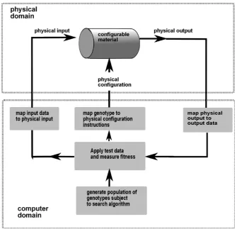
Evolutionary computation is a class of algorithm for global optimization inspired from a biolog-ical evolution. Just as how a set of species change their physbiolog-ical properties to adapt better to the environment over the generations, evolutionary computation utilizes set of solutions, alter them, and make them closer to the global solution. This chapter will begin with the notion of the evo-lution followed by genetic algorithm in terms of computer science concept. This computation can be realized in the material system rather than in the software platform. Such concept known as Evolution in Materio is later theorized to ensure the reader is aware of the conceptual notion behind this thesis.
2.2.1 Natural Evolution
pressure gives advantage to the more adapted ones by being able to out-compete others i.e. the unadapted, short-necked individuals gets weeded out and the best-adapted, long-necked ones survive. These variations become dominant in the species as it continues so it evolves. This ele-mentary example is, of course, highly speculative theory, and the idea that longer neck gave ben-efit in searching for the food has become a target of many criticisms[17, 18]. However, the main concept remains across most of the giraffe argument; the evolution process takes place over the generations and the new individuals are implicitly selected based on their fit to the environment. This natural process forms the basis for the development of evolutionary, or genetic algorithms.
2.2.2 Genetic Algorithm
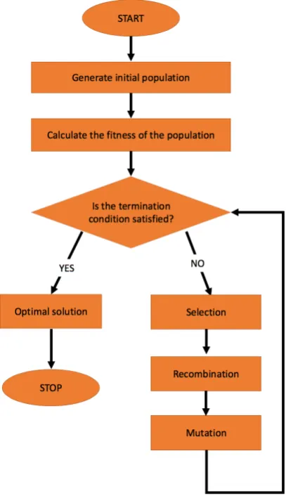
Genetic algorithm adapt some or all of the principles for solving search and optimization prob-lems. The basic process of genetic algorithm is illustrated in figure 6. A population of coded answers to a problem is randomly generated. The member of this population is ranked by a fit-ness function, and selections are made depending on their fitfit-ness scores. Some members of this population may be mutated, or recombined by shuffling their information content with the other member of the population. Mutation allows a randomly timed sampling of an even better result, and recombination allows implicit testing of combination of the the population members. As process recurs multiple times, the survival of the fittest principle drives the population to better average fitness scores, thus more optimal solution.
Figure 5:Conceptual image of natural evoltuion. Given species include both short and long necked giraffes, but the long necked one has higher chance providing offsprings due to its food advantage. Image taken from [19]
2.2.3 Evolution in Materio
Figure 6:Flowchart of simple genetic algorithm. Genotypes are evaluated to see how fit they are to the desired solution. If enough similarities are achieved, the solution search stops. Until then, the algorithm continues to alter the genes.
In this evolutionary form of function solving, the term genotype is used to the string of num-bers that defines a solution to a search problem (i.e control signals). These genotype has indi-vidual elements commonly referred as genes. Solving the computational problem is done by as-sessing how well the genotype represents a solution, or how close the output they provide is to the desired output. Survival of the fittest approach is implemented by sorting out these geno-types by the fitness scores, ranking their performance in the order, and choosing the genes so that the next generation are essentially more fit to the solution than the previous generation. This is conceptually visualized in figure 7.
The process was originally inspired by A.Thompson [21] who used unconstrained evolution to evolve working electronic circuits using a Field Programmable Gate Array(FPGA). In Thomp-son’s experiment, tone discriminator, a digital circuit that distinguishes signals of 1 or 10 kHz, was programmed using evolution procedure. It was concluded that the controlled evolution of the configuring bit strings could relatively easily solve this problem. However, the experiment lead to a discovery that the successful circuits found from the GA worked by utilizing subtle electrical properties of the silicon, which lead to a ongoing research interest of material based computing system, EIM.
material such as Liquid Crystal Display [22] or a cluster of metalic nanoparticles [2]. These prior research suggests that the physical systems, particularly ones that are high in complexity, are use-ful in genotype mappings as they can provide many ways of exploitable effects within the material system that can contribute to improved fitness.
3 Device Fabrication
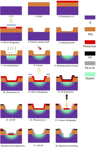
The fabrication scheme is an extension of CMOS device technology and is based on the single charge transport device made by Mueller et al [23]. The large part of the procedure will follow that of the 8 electrode spider design in the previous work by J. van. Gelder [3] and Bose et al [2]. Due to the non uniform nature of some of the procedures, it is not possible to create an indentical device with a same IV characteristics. However, achieving the already-known functionality does not require stringent electrical property, thus the device has rather large room of tolerance in its perfection.
The recipe starts with creating a doped region where the silicon will be bombarded with the dopant. The oxide are grown with a controlled thickness for the dopant window region so the de-sired dopant concentration is achieved only in that particular area. Pd electrodes are then created by patterning the resist using the photo-lithography technique and depositing Pd through an e-beam based evaporation chamber. The nano-electrodes are made in similar procedure but using electron beam lithography (EBL) to pattern the resist since it is a nanoscale structure, thus unpro-ducable with the conventional photo-lithography system. The materials used for the nanoelec-trodes will differ depeding on the dopant used. The steps recorded in this report are in a simplified format. The actual fabrication procedure includes numerous cleaning and baking steps which are necessary as a preparation procedure for the lithography, as well as ensuring the contamination level is low. It is also crucial to inspect the surface structure, particularly the depth, after the indi-vidual etching procedures. This improves the reliability of other fabrication processes by ensuring that the etched species are sufficiently removed. The fabrication process flow is depicted at the end of this section in figure 8. This process flow is a refined version of the previous recipe [3]. The changes made as well as the improved characteristics from those changes are discussed under the result section.
3.1 Oxide Growth
The one side polished intrinsic silicon wafer is coated with 200 nm of high quality oxide using the thermal furnace. Annealing was done at 1100oCwith sufficient O2gas flow. Ellipsometer was used to accurately determine the thickness of the oxide. This oxidation is followed by hydrogen annealing to passivate the dangling bond of the oxide layer, thus improving the quality of an insu-lator. 26§60µm rectangular window is etched by immersing the sample in a BHF(1:7) solution. This wet etching technique is known to result in an isotropic etched profile, a structure that gives an advantage during the processes explained later. It is however, necessary to be cautious of the overetching (i.e. removing too much SiO2, thus the sample should be placed no more than 4 min-utes, sufficient in removing the 200nm thick oxide window vertically.
3.2 Dopant Implantation
to hop is one of the crucial parameter of the device. The availability of free simulation software such as TRIM, as well as the abundance of previous studies makes it a more matured technique to qualitatively fabricate the device with high control of the dopant concentration. Ion Implan-tation, however, is not a diffusion-free technique. It is necessary to include high temperature annealing after the implantation as the damages into the silicon crystal from the high energy ion collision must be recovered, and the dopant also has to be activated into the substitutional lattice sites. This can be optimized using the rapid thermal annealing(RTA) procedure where wafer is annealed to high temperature in a very short time (seconds to miliseconds) and is cooled down rapidly without overly exerting the thermal stress to the wafer. This technique is known to mini-mize the dopant diffusion because of the shorter annealing time, without hugely compromising the amount of dopant activation[24].
For this thesis project, Boron was implanted as BF using 40keV energy and 3§1014i ons/cm2 dosage. Implantation was followed by etching away the 40 nm oxide layer that is grown on the dopant window region in prior for the masking purposes.
3.3 Micro-Lithography
Fabrication of the contact pads and the electrodes should follow the device doping. Using the same photolithography technique as the patterning of the dopant windows, the photoresist was exposed at where the contact pad material will be deposited. The fabrication of this contact pad structure must occur after the ion implantation as the high energy ions from the implantation pro-cess could damage the metal structure[3]. Upon development of the resist, few nm of Ti was de-posited as a sticking layer, followed by the Pd deposition, both on the entire surface using BAK600. By removing the existing photoresist from the surface, the sputtered material above the photore-sist will also be washed away since they are not bounded to the surface of the substrate. The deposition area with no photoresist, where the patterning and development occured, will retain the material. This procedure is known as lift-off, and can result in a structured metallic pattern such as the ones fabricated in this experiment.
3.4 Nano-Lithography
EBL is used to pattern the nano electrode. This technique "writes" on the PMMA negative pho-toresist by high energy electron bombardment, resulting in very small yet precise feature im-printed on the resist. Upon developing the pattern, nano electrode material can be deposited using Bak600. The electrode structures are present once the PMMA resist has been "lifted-off". At this moment, this electrode has to bridge the dopant window and the Pd contact pad. The wet etching of the oxide had resulted in a sloped oxide structure in contrast to the very sharp vertical wall which is produceable by the other etching technique, dry etching. Thus the nano electrodes can be reliably made without requiring to be deposited on the vertical photoresist side walls. The deposited metals must be chosen based on the dopant element. As later explained in the result section, the surface resistance becomes a hindrance when characterizing the dopant device un-der the low temperature. As such, the contact resistance arising from the difference between the dopant energy level and the metal’s fermi level must be minimal in order to create an efficient device.
3.5 Post-Etching
nano electrodes, Si surface is etched until the surface concentration is reduced to the insulating regime where the hopping conduction can occur. Previously mentioned wet etching is not suit-able because the isotropic etching profile will result in the undercut of the silicon, thus there is a risk of etching away the metallic Si underneath the electrodes, or worse, completely separating the Si from the electrodes by overetching. Therefore the reactive ion etching (RIE),also known as plasma etching, is implemented. RIE is done in a vacuum chanmber filled with a reactive gases. These gases are excited via RF field and produces excited and ionized species that are both impor-tant for the etching process. The former can chemically etch away the desired material owing to its high reactivity, and the latter is accelerated by the RF field and impart energy directionally to the surface. The process results in more anisotropic etching profile than the wet etching process due to the sidewall passivation, typically achieved by introducing a carbon-containing fluorine species to the plasma[25]. This makes it a suitable for the highly vertical walls as well as when an accurate reproduction of the photoresist dimensions are needed on to the structure.
For this experiment, the pressure of the TEtske RIE chamber was maintained at 10mTorr and the RF power at 60 W. CHF3, and O2, flow were set at 25 and 5 sccm respectively. These flowrates can be varied to achieve different etch rate for SiO2 and Si[26]. For the purpose of this experiment, this flow rate is sufficient to etch Si at approximately 40 nm/min rate. This can be done for vari-ous duration to achieve the desired surface dopant concentration which will ultimately relate to the operational temeprature.
However, RIE process will not give nanoscale precision due to the slight variance in each processes (cleaness of the chamber, sample location on the holder, etc.) Therefore, the technique should be used in combination with the topological analysis such as Atomic Force Microscopy(AFM) in or-der to qualitatively monitor the etched profile.
3.6 Post fabrication treatment
4 Experimental Setups
4.1 Boolean Logic
The searching for boolean logic in the disordered system was originally accomplished by Bose et al[2]. The two input and one output requisite of the conventional CMOS is translated in our device as using two electrodes as input where a specific waveform is sent, and one as an output which is used to read an output current varied from the input amplitude and the value of control voltages, which is assigned to the remaining 5 electrodes. These control voltages can locally manipulate the potential landscape of the device and alter the percolation path of the electrons from the input electrode to an output electrode. Thus depending on the control voltage values, unique and rich input-output relations can be obtained, and this relation landscape is explored using the genetic algorithm to find a global minima a.k.a function to be solved.
4.1.1 Fitness score calculation
Referring to the theory section, the control voltages are recorded as genes, and complete set of genes(V1ªV5) are referred as genomes. The fitness score (F) will be calculated for each genomes by comparing how closely the output Y satisfies the ideal output X. In contrast to theory, the points of signal transition can lead to unexpected spike or dip in the output, thus these points will be effectively ignored by assigning lower weights W at these areas. For the remainder of the signal that consitututes the output, Y and X are computed as:
Y =mX+c
by estimating the magnitudemand the offsetc. High signal to noise ratio as well as low offset is desired for the good output, thus the fitness score is defined as:
F=p m
r+±|c|
where delta is a mixing parameter and r is the residual error, thus SNR is (m/pr). Further pa-rameters can be used to characterize the fitness score, the modified fitness function is defined as:
F=A§prm
+±|c|+B§ 1
r +C§FQ+D§Novel t y where theFQis the fitness quality which can be defined as:
FQ=mi nmax1°max0
1°mi n0
where min and max is defined as the minimum and maximum of the signalIout(t) at the time
sequence when the signal corresponds to high(f(t)=1) or low(f(t)=0).
The numerator of the fitness quality is a tolerance parameter which is normalized by the full spectral range(max1°mi n0). This method ensuresFQ<1 yet doesn’t take in account of the offset
ofmi n0, thus this penalty factor is subtracted from the denominator to redefine the fitness quality as:
FQ=maxmi n1°max0
1°mi n0+ |mi n0|
4.1.2 Breeding mechanism
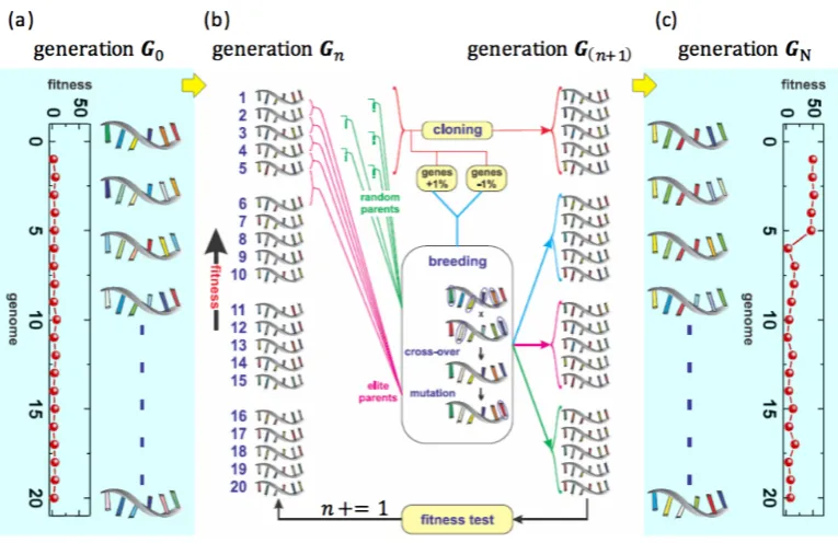
Each generationGn consists of set of genomesg=Gn,i for 1<i <mthat have different fitness
scores. Just like the natural selection, it is in the best interest to preserve the genomes that perform well and abolish the underwelming ones for the sake of improving the entire species. For a set of 20 genomes, 5 best performing ones directly proceed to the next generation. The 5 following best ones (6th to 10th best) are slightly modified by±1% and bred asG(n+1),i=Gn,j§Gn,kwhich
consists of a uniform crossover with a mixing ratio of 0.5 in which each genegl of the offspring
g=G(n+1),iis assigned randomly from either parent geneGn,j,lorGn,k,l. Similarly, the following 5
genes are crossover of the five best performing genes with its follower (Gn,i§Gn,i). The final set of
genes, ones that are not likely to survive, go through chance of mutation in which they are given a random value with a probability of 0.1. ThusGnis sorted in the descending fitness order and the
next generation is created as followed:
G(n+1),1!G(n+1),5=Gn,1!Gn,5
G(n+1),6!G(n+1),10=G+n,1%i §G°n,1%i
G(n+1),11!G(n+1),15=Gn,i§Gn,i
G(n+1),16!G(n+1),20=Gn,i§R ANDOM(Gn)
[image:26.595.111.494.376.624.2]Whereiranges from 1 to 5. Illustration for this breeding mechanism is shown in figure 9.
Figure 9:a) The GA starts with a random initial generation. (b) Many cloning and intercrossing processes are done until (c) a final generation is reached. The genome with the highest fitness should have a higher fitness than any genomes from the first generation,G0.Image taken from [28]
4.1.3 Multiple Boolean Logics
are: IQ test and full-search. IQ test is a quick method where all the input output configuration can be invariantly tried in a speedy manner to get an estimate idea of how “smart“. This is done by applyingVH IG H=1V orVLOW=0V to every electrodes while the one electrode is assigned as
an output; forming 27=128 voltage configurations. Such method tests the variance in the type of logic obtainable from the set of binary electrode configurations. This can be an efficient method in detecting if a device has a certain boolean logic since it takes less than an hour to try all the voltage configurations for every electrodes as an output. However, it lacks the measure of the abundance as well as the quality of the boolean logic it can find since the applied voltages are fixed to 1V or 0V. Another method is a full-search which generates over thousands of randomly chosen voltage configurations and tests them as one generation. Each output waveform is fit into the 16 solutions, and checks the abundance of each solutions within the devices by creating a plot of the logic abundance with respect to the fitness. This time consuming method can indicate the smartness of the device by showing all boolean logic result which it managed to output with the fitness score taken into account. Previous experiments by Van Gelder [3] have shown that the boolean logic can be found on the arsenic dopant device without utilizing all five control volt-ages. Therefore, it should be in the next scope to determine how far the 8 electrode device can accomplish in the new goals, rather than determining how well they do in the already established benchmarks of single boolean logics.
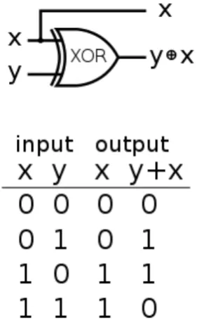
[image:27.595.229.370.426.663.2]Control NOT gate (CNOT) is a standard basis for a two-qubit quantum logic gate. It flips the second bit only when the first bit is HIGH, and leaves it otherwise when the first bit is LOW[29]. The classical representation of CNOT gate is shown in figure 10. It can be treated as two-input-two-output system where two outputs should be a follower of the control input, and an XOR gate. Rather small change is necessary from the conventional boolean logic search in order to aim for
Figure 10:Classical representation of Control NOT gate. The target signal y is reversed only if the control x is 1
one input and one output, with however many control voltages that it is assigned to the remain-ing electrodes. One electrode from each device wil be used as a bridge for control signal to talk to the input signal. Such method slightly deviates from the goal of challenging the intelligence of the singular device. However, the conceptual goal of achieving higher functionality than the “Standard” boolean logic is still within the scope. Optimizing such logic requires another layer of
Figure 11:Device setups for the CNOT gate. a) For a single device, it is only a matter of assigning one of the control electrode as an output. The location of control, input, as well as output can be arbitrary. b) Two device setup in which each device has an input and an output. Bridging exists beteen two devices for the control signal to interfere with the input signal
fitness calculation from the previous formula:
Fover all=E§F1+H§F2
where the overall fitness scoreFover allis calculated as the sum of the fitness scores of the
individ-ual output with an assigned weight E and H on it.
4.2 Darwin internet
The logic functionality can be done using few transistors, yet the real computing power of modern laptops and smart electronics are due to the billions of transistors working in parallels. It is thus within the possibility that the dopant network can have higher functionality from incorporating multiple devices. As the dopant network is a designless reconfigurable device, it is unlikely that it has the same scalability as the conventional CMOS devices. However, more complex informa-tion/tasks than the boolean logic may be processible by creating an interconnecting network of the dopant devices. This section will be dedicated to the concept of the scaled up system and its experimental setups. The experiment aims to evolve the “interconnectivity” of the dopant internet to achieve functionality. This is within the scope of the overall project to achieve the “scaled-up” functionalities.
4.2.1 Theory: Interconnectivity
The external research estimates that a human brain can have 20 billion neocortical neurons, with an average of 7000 synaptic connections each[30]. The intelligence and the brain capability is tremendous owning to this colossal number of principal units. However, the wiring of synapses play a crucial role in the decision making from the firing activity[31]. The schematic to utilise this interconnectivity in realising functionality is shown in figure 12. 8 electrodes of the first device can be connected to the intermediating layer which from here will be referred as an interconnect layer, and there areNI=8 layers.
ForNC number of devices in the network, every one of them hasNI electrodes which can
Figure 12:Design schematic of the interconnections between the devices. Image taken from [32]
is closed and 0 is Open). This can be represented by an interconnectivity matrixW =NI§NC.
These interconnect layer can also be connected to the power source as well as the readout sensor, thus another binary matrixWB andWOare used to represent the connectivity to those terminals.
There are thus 2NI possibility for the switch states of the power and readout matrix, combined
with the interconnectivity matrixW, allows the network to have 2NCNI+2NIconnectivity. Referring to figure 12, a current through the network can be wired across any devices, thus each wiring con-figuration can create a different recurrent neural network(RNN) where the internal states are the electrode voltages. The setup is theoretically possible to deal with time-varying signals if the in-put is also time-varying. However, it can also be used to obtain a stable current outin-put for certain functionality such as classification. Thus the setup is reduced into a simple feed-forward neural network. This neural network modelling of the dopant internet is illustratively shown in figure 13. With such modelling in mind, any neural network functionality should, in theory, be possi-ble with the dopant internet setup. The applied voltages on each electrode can be tuned by the
Figure 13:Illustrated model of RNN and FNN. RNN have a recurrent signal path where as FNN have a forwarding signal path with no signals returning to the previous nodes. Image taken from [28]
[image:29.595.230.369.550.697.2]14. Rather than directly applying a desired voltage value to the electrode from the power source as demonstrated in the logic search setup, the connection from the source to the electrode can be manipulated with the switch configuration, thus applying a different value of voltages with-out requiring multiple sources. In the figure 14 example, it is possible to changeIout1andIout2 at their electrodes by manipulating the bias at its neighbouring electrode whose connectivity is controlled by switch A and B. By changing the switch configuration such that the switch A is ON, its respective electrode will acquire different bias because the distance from the source,Vi n has
now changed. This wiring configuration can be evolved by controlling the switches using genetic algorithm. For a setup withNC=8, there are 28§8+2§8º1.2§1024º1024wiring configurations.
Suppose the source and the sensor electrodes are chosen for all 8 devices, wiring configuration is reduced to 264º1019. This number can be further reduced by realizing that there will be some
Figure 14:Illustration of difference that the switching can make. The output current recorded from twoIouts are dif-ferent depending on the state of their respective switches because the current path from theVi nwill change drastically.
degenerate configurations with respect to the current-voltage relations. However, in practice, it is difficult to assume the exact reduction due to the resistance variance amongst devices as well as the asymmetry of the Coulomb gap between the electrodes under low-temperature condition. Nevertheless, with correctly determining the desired output, the large area of the search dimen-sion is irrelevant as genetic algorithm should slowly yet deterministically “figure its way out“.
4.2.2 Theory: Pattern Recognition
The fundamental principle behind the classification task is “If X is satisfied, then Y”[33] where X is the antecedent of the rule and is formed from a set of conditions and Y is the consequent of the rule, i.e. predicted class. This can be applied in various ways to define own classification rules. For a specific input, only one output has to be responsive to be able to classify the information on the input. This will be incorporated in the interconnectivity experiment. For the purpose of our experiment, dopant internet withNC =8, interconnectivity matrixW will consist of input,
output, and interconnect layers as seen in figure 15 b).
In this context, if the digit 1 is implemented, the pixels that constitutes 1 is mapped in the matrix such thatW1b=W1e=W1h=Wc2=Wf2=1 and the rest is 0.WB is set as {1,1,0,0,0,0,0,0}
which connects battery only to the input layer andWois set as {0,0,0,0,0,0,0,1} such that the last
row of matrixW is the output layer. The remaining row is used for the weights of the hidden layer. For example, the output node h8 can recognize the digit 1 if there is a flow of current after setting W8h =1 only if the input image looks like a 1. In a similar manner, if the nodesa8 tog8 can
Figure 15:Conceptual image of 3 by 5 digit classification a) digit from 1 to 8 can be represented with 15 pixels b) which can be translated as an input, and be shrinked down to 8 output. c)Only two kinds of logic are necessary to uniquely recognize the output d) Realization of c) with the actual network. Image taken from [28]
4.2.3 Practicals: Switch experiment overview
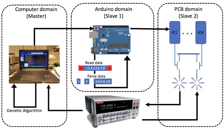
Overview of the whole switch experiment can be seen in figure 16. The process begins with the 8 by 8 array of booleans. The individual segment of the array corresponds to a particular switch from the ICs. Thus by setting that boolean to true, the switch will connect the corresponding electrode to the interconnect layer. This interconnect layer is a floating metallic island, and the access can be shared by the same electrode of 8 different devices. Furthermore, by connecting to the input of the current source unit, Keithley2400, the voltage can be applied from any of the interconnect layers. Similarly, another interconnect layer(not the same one as the input, for an obvious reason) can be connected to the output of the Keithley2400, thus the current value can be recorded from any of the interconnect layers. This interconnect layers that are connected to the battery and the sensor will be referred to a source layer and a sensor layer. Suppose a partic-ular switching configuration is in effect, the current from any particpartic-ular output electrode can be detected by ensuring the switching such that only that electrode is connected to the sensor layer. Thus by sweeping switch configuration so every output electrodes are singularly open, multiple Iout’s can be obtained.
WithNC=8 and one sensor layer, it is possible to classify 8 different inputs provided that
1. For every input, one output electrode is HIGH
2. The output electrode is HIGH for only one particular input and LOW for the other input combination
out-Figure 16:The image overview of the whole protocol. Arduino bridges the Computer and PCB domain to translate the instructions.
put is HIGH, then the system simply did not understand what the input is. While more than one output being HIGH indicates that the system could not differentiate the input from two possible solutions out of the eight. The second requirement corresponds to the network’s ability to sepa-rate the solution. If an output electrode is HIGH for two different inputs, it means that the system can not differentiate two different inputs (e.g not being able to find the difference between 3 and 8.) As such, the system with N different input and M different outputs (one source layer and sen-sor layer) will have an output arrayWN Mwhere the individual item in the array corresponds to the
detected current at the electrode of the device M from a particular switch configuration with the Nth input. What is considered HIGH and LOW are ambiguous and can be tuned depending on the experiment. For this experiment, all the current values will be normalized with with the highest value of current from the respective rows and columns. A certain percentage value can be set to determine the threshold value which distinguishes the HIGH and LOW. By setting this threshold value low, the condition to achieve singularity is also harsher because the range of values that can be considered HIGH with respect to the maximum value broadens. The evaluation method using the HIGH and LOW status of the output is explained in the next section.
[image:32.595.82.510.75.323.2]Figure 17:5 by 5 output array showing the current value in nA where a) box in yellow indicates the row-wise highest value. a)If threshold =0.9 ,b) =0.8, blue is indistinguishable from the highest, first row now unsatisfies the requirement. c) At threshold of 0.5, red is also indistinguishable. No rows from the output array meet requirement (1) d) The array from a), but green is the column-wise highest value. Orange is where both requirement(1) and (2) are satisfied, hence classifiable.
4.2.4 Practicals: Experimental procedure
1. Generate initial populations
2. Calculate their fitness
3. Select the fittest of the population
[image:34.595.165.427.180.495.2]4. Recombine/mutate
Figure 18:Illustration to indicate the flaws in generating genomes randomly. a) Some rows are irrelevant in the va-riety(row1 and row 5), or effectively meaningless(row2). b) The physical meaning of what row 2 and row 3 does. The situation in row 2 is effectively the same as having no switch ON
With the above concerns, the following procedures are taken in the modified code for the full search experiment:
1. Randomly generate arrays
2. Transform the input/output rows to zero
3. Transform all column with no device to zero
4. For the columns unaffeected from 3, check if any rows have only one 1s
5. Go through all the genomes for a duplicate check
If any genomes are flagged from item (4) and (5), they are scratched and another array is ran-domly generated and goes through the procedures again until all the genomes satisfy above con-ditions to ensure the variety amongst them. This elimination of invalid switch configurations can reduce the number of possible configuration to:
(2NC°N C)
2NC §2NI§NC°(NB§NS)§NC
WhereNB andNS is the number of rows used for the input and output respectively. The factor
in the exponent takes care of the reduced switch configuration from neglecting the input/output row state. The fraction represents the reduction from eliminating the only one connection per row situation.
Referring to the switch overview chapter, every genomes will come with a certainWN Moutput
current array. For the purpose of evaluating the genomes, this array must be converted to a certain fitness score to determine how close they are to the ideal solution. This experiment will use two values; fitness score and success number. Fitness score is calculated by normalizing with respect to the highest value from the row. For every element, their absolute value status is determined as:
(IOU TAB /ImaxA )
Tolerance =
(
H IG H, i f ∏ 1.0
LOW, i f < 1.0
WithIOU TAB being the output current at row A and Column B,ImaxA is the highest output current value from row A, and tolerance is a parameter that determines the threshold value for HIGH and LOW. This checking will be done to every item in row A of the output array. When only one item is labelled HIGH, the output row A has no current that can be considered HIGH in respect to the highest value from that row apart from the highest one itself. Therefore, when this counter is one, fitness score adds 3 points to itself, indicating a successful one-to-one input-output relation; F i tness=F i tness+3. For a scenario where more than two are considered HIGH, fitness score subtracts a point for x number of HIGHs that were counted;F i tness=F i tness°xF i tness.
This fitness score only focuses on whether for a particular input, more than one output was sufficiently responsive or not. To truly determine the unique input-output relation, the output array must be a permutation matrix, where exactly one entry of 1 in each row and each column and 0s elsewhere. Firstly, the highest value from row A of the output array is pointed. Then the column list of that value is also scanned, and check whether the IOU TAB is the highest from the column B. IfIOU TAB represents the singular highest value from both row A and column B, then it can be defined as a successful classification, hence the success number is incremented by one:
ImaxA =? ImaxB
(
Once all the genomes of the generation have been evaluated, they are ranked in the descend-ing order of the fitness score. Currently designed selection procedure selects one genome who had the highest score, and the rest are discarded. The 4/5 of the new population is reborn as a mutation of this sole winner. The copy of this winner array is made, then by every bit, they are given 30% chance to switch their boolean state. The remainder of the new population is an en-tirely new genome, randomly generated like the initial population.
The python code to implement the entire procedures is available on the skyNEt github repos-itory. Here a pseudo-code is included to give the reader a general idea of the GA process.
Algorithm 1Interconnectivity Experiment
1: procedureSWITCHEXPERIMENT
2: i,j√generation, genome 3: SwitchConfig√initial pop
4: Make Connection to Arduino and Keithley: 5:
6: fori number of timesdo 7: forj number of timesdo
8: Record the output current
9: Evaluate their score
10: Choose the winner
11: Mutate the rest
4.2.5 Practicals: Dipstick development
To carry on the switch experiment, entirely new model of dipstick had to be developed since the number of electrical connections as well as the mounting PCB is vastly different from the con-ventional dip sticks used in NE lab. The early model of the dipstick designed for the intercon-nect experiment can be seen in figure 20 a). The samples will be wired on the PCB which will be mounted on the dipstick with a sealed vacuum can located at the right side of the stick in the figure 20 a). This PCB can communicate with the master unit, Arduino, through the wiring in the hollow metallic pipe. At the end of this wire, a necessary number of connections are made to the Arduino to configure switching configuration.
Figure 20:a)The initial model of the dipstick designed for the switch experiment. b) The final model of the dipstick. The hole has been drilled to the can and headpiece has been attached.
unprotected. The solution to this sealing can was met simply by drilling a hole to keep them con-nected using a screw. Another hole was drilled at the bottom of the can to allow a flow of liquid Nitrogen to touch the sample such that no atmosphere particles are present when cooling down. This leads to exposing the electronics to a liquid, yet the sealing can still protects the PCB and the samples from unwanted collisions when inserting/extracting the dipstick. This will produce a vaporized Nitrogen inside of the dipstick rather than the outside. Thus an escape path from the PCB to the outside of the vessel was necessary. Apart from the ribbon cable, the dipstick is made with a hollow tube which should be more than enough to ventilate the built-up pressure within the dipstick. However, due to the number of aluminium soldered electrical connection, as well as the presence of Arduino UNO, better option was to not expose the sensitive components of the experimental setup to a blast of pressure ventilation. This problem was solved by first filling the hollow space of the dipstick with a silicon paste to avoid the flow of gas, and then inserting an exhaust tube to directly connect the top of the hollow tube area to the atmosphere. Such measure allowed the airflow from the top of the hollow tube, where the nitrogen gas is expected to accu-mulate, to the atmosphere without having the electronics in contact with the gas. The simplified schematics of the inner component of the dipstick can be seen under figure 21.
4.2.6 Practicals: PCB development
The PCB used for the boolean logic experiment can support one device and eight electrical con-nections to the control unit. The interconnect experiment will accommodate a maximum of eight devices and sixty-four electrical connections, individually allocated for every electrode in the de-vices. Thus a new type of PCB had to be created to support such experiments. The upgraded PCB seen in figure 22 was originally developed by a previous student who performed an internship at NE lab[32].
Figure 21:Simplified schematics of the top of the dipstick flat cables consist of a)eight signal line, b)Arduino signals and c)unused common lines. d)External grounding ensures the proper grounding. e)Exhaust line allows gas flow from the top of the hollow tube of which the flow to the electronic box is prevented by the f)red silicone paste. The size of the wires, headpart of the stick, as well as Arduino not up to the scale.
as well as their capability to be daisy chained for the purpose of serial data transfer. The working of these chips can be regarded as an 8-bit shift register. Each ICs are responsible for controlling eight switches on the board, thus the 8-bits information that is transferred can be representative of the eight switches. This data first arrives at the first IC. The data output of this IC is connected to the data input of the following IC, thus when the second 8-bit information is sent, the first set of information is transferred to the second IC, while the first IC welcomes the arriving second set of the information. The process is done using Serial to Peripheral Interface(SPI) method which synchronously operates with the clock signal that arrives at the SCK(clock signal) or SCLK pin of ICs. When the last set of 8-bit information is sent, the first set of information arrives at the last IC, thus the new switch configurations are in ready to be reflected. The rising edge of CS(Chip Select) signal will trigger the switch to change to a corresponding new state.
Figure 23:a)MAX395 chip in Daisy chain b)Functional diagram c)Timing diagram d)Pin configuration. Images taken from [34]
As such, every ICs have pins that are connected to the SCK, CS, and Din (and Dout) for the SPI protocol, V+, V-, GND for the power, and NO pins that contain the switches for the every electrodes. These separate signals are treated by independent pins from PCB as seen in figure 24. The pins with S label corresponds to the signal line, and C for the common line. For the requirement of the interconnect experiment, no common signals are necessary, thus all the C pins will not be used.
4.2.7 Practicals: Software development
Figure 24:The sideview of the PCB in figure 22, shown with the labeling for each pins.
cycle or instructon every 62.5 nanoseconds. For serial communication with baudrate of 115200 (baud means bit per second), 14400 byte of information can be sent per second, or 1 byte per 70 microseconds. In the time it takes to transmit 1 byte of information over the serial line at 115200 baudrate, Arduino will execute approximately 1120 instructions. This requires some form of synchronization of Arduino and the incoming data to let Arduino know when all the data is there to be processed. The method used in this experiment will utilize the starting and ending marker to control the Arduino’s data reading. Before sending the 8-byte information, PC first sends the starting marker character. This will trigger the readout function of the Arduino, thus the information sent after the starting marker will be stored in Arduino’s buffer, but not before. When all the data is sent from PC, the end marker character is sent to finish the transmission process. Upon receiving this character, Arduino will go out of the readout state, thus can proceed to process the information. For the purpose of this experiment, < and > are used for starting and ending marker respectively. In theory, any characters that are not number nor comma can be used
Algorithm 2Arduino algorithm for marker based receiving
procedureRECEIVEDATA
2: recvInProgress = False√Boolean flag = False√Boolean2
4: rc√received character
whileData is available and flag is falsedoAssign the data to rc
6: ifrcis<then
recvInProgressisTrue
8: ifrecvInProgressisTruethen ifrcis not >then
10: Store data in the buffer
else
12: Terminate receiving
recvInProgress = False
for the markers. This functionality is illustrated in a pseudo code 2. While the data is available to be read on the serial line, any detected character is read and stored inrcvaluable. The reading process starts only whenrecvInProgressflag becomes true which is only possible if the received character is a starting marker, <. The process terminates when the received character is an ending marker, then therecvInProgressflag is reversed andnewDataflag becomes true to move out of the while loop.
Arduino receives information by individual characters. Suppose the 8-bit 11111111 is sent to Arduino in a byte as 255, Arduino buffer will not receive 8 1s nor 255 as a three digit number, but the character 2 followed by 5 and then another 5. To correctly reformat this into 255, data parsing has to be done on the Arduino side. strtok() function from C library can be used to parse the strings. Such function will split the set of strings into tokens which are sequences of characters separated by the delimiter parameter. The function will initialize the pointer at the first character within the temporary array which is copied from the Arduino buffer. Then continue down the buffer until the delimiter character is detected, and then tokenizes whatever set of characters are found until then. This is immediately followed by atoi() function which converts the string into an integer, the variables usable by SPI communication protocol, and then stored in the switcharray which will be used to send 8-byte information to the PCB.
Algorithm 3Arduino algorithm separating data to bytes
procedurePARSEDATA
Strtok√Temporary array of chars 3: ifflag is Truethen
Collect the char fromStrtok
ifchar is “comma”then
6: Tokenize the string
Convert to integer Assign it to switcharray
![Figure 1: Semiconductor band diagram consisting of conduction band(EC), valence band(EV), and the energy levelsof the donor and acceptors (ED,A)[7]](https://thumb-us.123doks.com/thumbv2/123dok_us/9686655.470055/11.595.216.367.528.609/figure-semiconductor-diagram-consisting-conduction-valence-levelsof-acceptors.webp)
![Figure 4: Summary of temperature dependent conduction of doped semiconductor. The density of the states at eachregime are located.[8]](https://thumb-us.123doks.com/thumbv2/123dok_us/9686655.470055/17.595.184.420.90.349/figure-summary-temperature-dependent-conduction-semiconductor-density-eachregime.webp)
![Figure 12: Design schematic of the interconnections between the devices. Image taken from [32]](https://thumb-us.123doks.com/thumbv2/123dok_us/9686655.470055/29.595.230.369.550.697/figure-design-schematic-interconnections-devices-image-taken.webp)