Advanced Burst Mode Control to Reduce the Standby
Power of Flyback Converter
Min-Sung Kim
1, Hyoung-Woo Kim
2, Ji-Hye Jang
1, Ki-Hyun Kim
2, Kil-Soo Seo
2,
Nam-Kyun Kim
2and Young-Hee Kim
11: Department of Electronic Engineering, Changwon National University, Changwon, Republic of Korea 2: Power Semiconductor Research Center, Korea Electrotechnology Research Institute
28-1 Sungju-Dong, Sungsan-Gu, Changwon, 642-120 Republic of Korea Email: [email protected]
Received 2013
Abstract
This paper we proposed advanced burst mode control technique to reduce the standby power consumption of the switch mode power supply (SMPS). To reduce the standby power consumption, most of the converter use burst mode or skip mode control technique. However Conventional standby mode control techniques have some problems such as audible noise and poor regulation. In proposed techniques, basically, the burst mode control technique is employed to reduce the fundamental switching frequency while limiting the peak drain current. But, in proposed technique, to improve the regulation characteristic, burst period of the proposed technique is shorter than that of the conventional burst mode technique. And also, to reduce the switching loss increase due to the short burst period, burst switching signal of the proposed technique is partially skipped. By using proposed advanced burst mode control technique, calculated standby power is 0.695W while standby power of the conventional burst mode control is 1.014W.
Keywords: Standby power, Flyback converter, PWM IC, SMPS
1.
Introduction
Many electrical and electronics devices operate in low power or standby power mode, in readiness for an exter-nally activated signal. This external signal can be acti-vated by remote control, network connection, etc. Re-cently, the standby mode is widely adopted for many kinds of applications as users require devices that are always available and can be remotely turned on and off. Electronic devices operate in standby mode are always on and consumes some electric energy required to supply the micro-controller and other standby circuitry [1].
According to the report from Lawrence Berkley Na-tional Laboratory (LBNL), the standby power in many countries accounts for more than 10% ~ 15% of national residential electricity use [2-3].
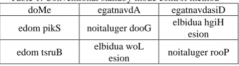
Due to the necessity of standby power reduction in electronic devices, many kinds of standby power control techniques such as burst mode control, skip mode control, etc., were invented. However, these kinds of techniques have some disadvantages as shown in table 1 [4].
In this paper, advanced burst mode control technique to reduce the standby power consumption is proposed. In proposed techniques, basically, the burst mode control
[image:1.595.303.544.588.655.2]technique is employed to reduce the fundamental switching frequency while limiting the peak drain current. But, in proposed technique, to improve the regulation characteristic, burst period is shorter than that of the conventional burst mode technique. And also, to reduce the switching loss increase due to the short burst period of the proposed technique, burst switching signal is par-tially skipped. By using proposed advanced burst mode control technique, calculated standby power is 0.695W while standby power of the conventional burst mode control is 1.014W.
Table 1. Conventional standby mode control method
doMe egatnavdA egatnavdasiD
edom pikS noitaluger dooG elbidua hgiH esion
edom tsruB elbidua woL
esion noitaluger rooP
2.
Power loss of the converter
op
l oss
VCC
I
P
=
×
st ar t l oss R VCC Vi n P 2 ) 2 ( − =
mode, most of the power loss comes from passive com-ponent such as resistor, inductor etc., and switching de-vice such as power MOSFET. Generally, because of the fundamental characteristics and poor controllability of the passive component, power loss of the passive com-ponent is hard to reduce. Therefore, most of the standby power reduction techniques focused on reducing power loss of the switching device. In this section, we analyze the source of the power loss of the converter and pro-posed novel standby power control technique to reduce the standby power loss without characteristic degradation of the converter.
AC input Output Power MOSFET Drive signal Rsense Rstart VCC Vsense Control IC Feedback signal
Fig. 1 Conventional AC-DC flyback converter
2.1. Source of power loss
Power loss in start-up resistor
Before PWM IC begins operating, the VCC capacitor is charged through the start-up resistor (Rstart). And this
resistor consumes power when PWM IC starting. Equa-tion (1) shows the power loss in start-up resistor.
(1)
Switching loss from switching device
When converter operates in standby mode, due to the switching loss from switching device such as power MOSFET, converter consumes standby power. Switch-ing loss is comprised of drivSwitch-ing loss from the gate drive circuit of the PWM IC and capacitive turn-on loss from power MOSFET.
Driving loss depends on total gate charge, gate to source voltage and operating frequency.
(2)
And capacitive turn-on loss depends on MOSFET out-put capacitance, drain to source voltage and operating frequency.
(3)
Power loss in PWM IC
PWM IC also consumes standby power and it depends on operating voltage and current.
(4)
[image:2.595.74.271.242.361.2]Table 2 shows specification of the commercial switch-ing device and control IC for flyback converter. By usswitch-ing this specification and equation (1) ~ (4), we can calculate standby power loss of the conventional flyback conver-ter.
Table 2. Simple specification of switching device and control IC
gnihctiwS ecived
Output capacitance : 200pF Input Charge : 63nC Rds(ON) : 0.85 ohm
CI lortnoC
Driving signal voltage : 15V Operating frequency : 50kHz
Duty ratio : 87% Operating current : 3mA Start-up resistor 200kohm
Calculated standby power loss of the conventional flyback converter is about 1.014W.
2.2. Conventional standby power control
technique
Start-up circuit
As mentioned in the previous section, start-up resistor consumed power when PWM IC starting. To reduce power loss from the start-up resistor, it is needed to replace it to internal current source which consist of high voltage device such as JFET. Before PWM IC starting, the internal current source supplies the internal bias and VCC capacitor. After VCC capacitor is charged, internal current source is disabled and PWM IC begins switching.
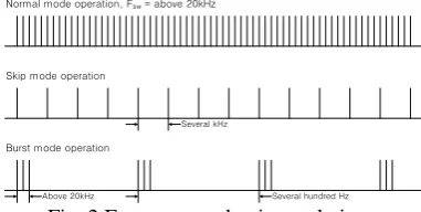
Reducing the switching frequency of driving signal Figure 2 shows reducing the switching frequency of the driving signal techniques which is widely used to reduce the switching losses in the power MOSFET and hysteresis losses in the transformer.
Normal mode operation, Fsw = above 20kHz
Skip mode operation
Burst mode operation
Several kHz
Above 20kHz Several hundred Hz
Fig. 2 Frequency reduction technique
sw gs gat e
l oss
Q
V
f
P
=
×
×
sw ds o
l oss
C
V
f
P
= × 2× [image:2.595.327.518.616.712.2]However, reducing the switching frequency lowers switching loss in power MOSFET, it also cause a problem such as audible noise or poor regulation of the converter output. To reduce the audible noise, it is needed to limit the peak drain current. However, it also lowering the converter efficiency. Therefore, the optimum value of peak drain current is determined by trade-off between converter efficiency and audible noise. And also, to reduce the poor regulation problem, it is required to increase the period of switching signal from several hundred Hz to several tens Hz or several kHz. But it may cause an audible noise problem or increase the switching losses.
Auxiliary power supply
If the power of the application is higher than 200W, due to the large output capacitance of the power MOSFET which used in high power application, reducing the switching frequency has limitation in lowering switching losses. Therefore, auxiliary power supply is used to reduce the standby power.
Output voltage drop or disconnection
Output voltage drop or disconnection techniques are also used to reduce the standby power of the converter. However, these kind of techniques have some problems such as high cost, lowering the converter efficiency, etc.
2.3. Proposed standby power control technique
As mentioned in the previous section, skip and burst mode control techniques have some disadvantages such as audible noise, poor regulation. Therefore, we pro-posed advanced burst mode control technique to over-come the problems of the conventional standby mode control techniques without increase of standby power consumption.
In the proposed technique, basically the burst mode control technique is employed to reduce the fundamental switching frequency while limiting peak drain current. However, to improve the regulation characteristic, burst period of the proposed technique is shorter than conven-tional burst mode control technique. But short burst pe-riod means switching losses of the proposed technique is higher than that of the conventional one. So, as shown in the figure 3, switching signal of the proposed burst mode operation is partially skip to reduce the switching losses. Averagely, minimum 60% of the conventional burst mode switching signal is skipped.
Figure 4 shows switching signal of the conventional (lower side) and proposed (upper side) burst mode oper-ation as a function of feedback voltage varioper-ation. When converter operates in standby mode, conventional burst mode technique generates switching signal when
[image:3.595.307.537.176.577.2]feed-back voltage decreasing phase (inside of the dashed line). However, proposed burst mode technique generates switching signal when both side of feedback voltage in-creasing and dein-creasing phase (inside of the straight line). So, regulation characteristic of the proposed technique is improved. And also, as mentioned above, switching sig-nal of the proposed burst mode operation is partially skip, standby power consumption is not increase.
Fig. 3 Switching signal of the conventional and proposed burst mode operation
Fig. 4 Switching signal of the proposed and conven-tional burst mode as a function of feedback voltage
3.
Schematic and simulation result of the
proposed burst mode control
[image:3.595.316.530.356.568.2]Fig. 5. Schematic of the proposed burst mode control
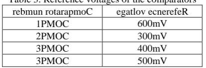
Table 3. Reference voltages of the comparators rebmun rotarapmoC egatlov ecnerefeR
PMOC
1 600mV
PMOC
2 300mV
PMOC
3 400mV
PMOC
3 500mV
PWM IC enters advanced burst mode operation when feedback voltage drops below 600mV. Switching contin-ues until feedback voltage drops below 500mV. And switching is partially skipped until feedback voltage drops below 400mV. After feedback voltage drops below 400mV, switching resumes until feedback voltage drops below 300mV. When feedback voltage drops below 300mV, switching stops and the output voltage of the converter starts to drop. This causes the feedback voltage to rise. When feedback voltage rises above 300mV, switching resumes. If switching skip period is long, feed-back voltage possibly rise due to the possibility of the converter output voltage drop. However, switching skip period is too short and switching resumes again before converter output voltage starts to drop. So, feedback tage drops until it passes 300mV. After the feedback vol-tage drops below 300mV, as mentioned above, feedback voltage rise. Burst mode witching starts when rising feedback voltage passes 300mV and continues until feedback voltage reaches 600mV. When feedback voltage rise above 600mV and converter still operates in standby mode (means light or no load), feedback voltage then falls and the advanced burst mode process repeats.
Simulation result
Figure 6 shows simulation result of the proposed burst mode control circuit.
As shown in the figure, when feedback voltage drops below 600mV, burst mode operation starts. And it con-tinues until feedback voltage drops below 300mV. As mentioned previous section, to reduce the switching
[image:4.595.310.534.193.374.2]losses, burst mode switching signal is partially skipped. By using parameters from table 1 and proposed ad-vanced burst mode control technique, calculated standby power is about 0.695W. However, about 60% of the cal-culated standby power comes from the start-up resistor. So, if we replace the start-up resistor to high voltage cur-rent source then calculated standby power may be lower than 0. 3W.
Fig. 6 Simulation result of the proposed burst mode control circuit
4.
Conclusion
In this paper, we proposed advanced burst mode trol technique to reduce the standby power of the con-verter. In proposed advanced burst mode control tech-nique, burst period is shorter than conventional burst mode control to improve the regulation characteristic and burst switching signal is partially skipped to reduce the switching losses. Calculated standby power consump-tions are 0.695W and 1.014W for the proposed advanced burst mode control and conventional burst mode control, respectively, yielding about 30% improvement in the standby power consumption. The standby power con-sumption can be enhanced to 0.3W for the proposed technique when start-up resistor of the converter is re-placed to high voltage current source.
5. Acknowledgements
[image:4.595.69.276.263.332.2]REFERENCES
[1] L. McGarry, “The standby power challenge” Proc. Of IEEE AGEC, pp. 56-62, 2004
[2] Alan Meier, Wolfgang Huber and Karen Rosen, “Reduc-ing Leak“Reduc-ing Electricity to 1 Watt”, The 1998 ACEEE Summer Study on Energy in Buildings, August 1998.
[3] J. P. Ross and Alan Meier, “Whole-House Measurements of Standby Power Consumption”, International Confe-rence on Energy Efficiency in Appliances, September, 2000.
[4] Hang-Seok Choi and D. Y. Huh, “Techniques to
minim-ize Power Consumption of SMPS in Standby Mode”, Power Electronics Specialists Conference2005, PESC, pp. 2817-2822, IEEE 36th, 2005.
[5] Yoh Matsushita, “Design for low electric power during standby state of fax-copier machine”, International Sym-posium On Environmentally Conscious Design and In-verse Manufacturing, pp. 391-395. 1999.