A Thesis Submitted for the Degree of PhD at the University of Warwick
Permanent WRAP URL:
http://wrap.warwick.ac.uk/94823
Copyright and reuse:
This thesis is made available online and is protected by original copyright. Please scroll down to view the document itself.
Please refer to the repository record for this item for information to help you to cite it. Our policy information is available from the repository home page.
Fabrication and Characterisation of
3C-SiC on Si Semiconductor Devices
Fan Li
School of Engineering
University of Warwick
Dissertation submitted for the degree of
Doctor of Philosophy
Contents
List of Tables iv
List of Figures v
Declaration xii
Acknowledgement xiii
Publications xiv
Abstract xvi
Nomenclature xvii
1 Introduction 1
1.1 Energy Crisis and Global Warming . . . 2
1.2 Power Electronics in a More Electric Society . . . 3
1.3 Silicon Carbide instead of Silicon . . . 5
1.4 Thesis Outline . . . 8
2 3C-SiC Properties, Growth and Characterisation 10 2.1 SiC Polytypes . . . 10
2.2 Electrical Properties . . . 13
2.3 Challenges for 3C-SiC Grown on Si . . . 16
2.4 Chemical Vapour Deposition . . . 19
2.5 Novel Techniques Reducing Planar Defects . . . 21
2.6 Physical Characterisation of 3C-SiC/Si Materials in This Study . . . 25
2.6.1 X-ray powder diffraction . . . 25
2.6.2 Atomic force microscopy . . . 26
2.6.3 Transmission electron microscopy . . . 27
CONTENTS
3 Electrical Activation of Nitrogen Implanted 3C-SiC(001)/Si 30
3.1 Intentional Doping of the Semiconductor . . . 31
3.2 Doping Level Characterisations . . . 34
3.3 Post-Implantation Activation of SiC . . . 36
3.4 Electrical Activation of Nitrogen Heavily Implanted 3C-SiC(001)/Si . . . 38
3.4.1 Experimental details . . . 39
3.4.2 Implanted 3C-SiC surface morphology . . . 42
3.4.3 Doping profiles by SIMS measurements . . . 42
3.4.4 Room temperature I-V measurements . . . 43
3.4.5 Temperature dependent Hall-effect measurements . . . 48
3.5 Summary . . . 53
4 Ohmic Contact on n-Type 3C-SiC(001)/Si 55 4.1 Metal/Semiconductor Interface: Classic Theories and More . . . 56
4.2 Contact Resistance Evaluation Tools . . . 65
4.3 A Review of 3C-SiC Ohmic Contacts . . . 69
4.4 Ti/Ni Ohmic Contacts on n-Type 3C-SiC(001) . . . 72
4.4.1 Experimental details . . . 72
4.4.2 Electrical characterisation . . . 73
4.4.3 Surface morphology and microstructure at the metal/3C-SiC interface 77 4.4.4 Silicide phase at the metal/3C-SiC interface . . . 82
4.5 Summary . . . 84
5 Study on 3C-SiC/SiO2 MOS Interface 86 5.1 MOS Technologies: Theories and Applications . . . 88
5.1.1 Ideal MOS interface . . . 88
5.1.2 Working principles of MOSFETs . . . 91
5.1.3 Degradation of channel mobility . . . 93
5.1.4 Charge effects at the MOS interface . . . 95
5.1.5 SiC/SiO2 interface traps . . . 98
5.1.6 SiC/SiO2 interface treatments . . . 102
5.2 MOS Interface Characterisation Tools . . . 108
5.2.1 Capacitance-voltage method . . . 108
5.2.2 Terman method . . . 114
5.2.3 High-low method . . . 116
5.2.4 Conductance method . . . 118
5.3 Dit study of 3C-SiC/SiO2 interface . . . 120
5.3.1 Experimental details . . . 121
5.3.2 High frequency C-V characterisation . . . 125
CONTENTS
5.3.4 Conductance method characterisation . . . 131
5.3.5 Comparing Terman, high-low and conductance methods . . . 137
5.3.6 High temperature effects on the 3C-SiC physical features . . . 138
5.4 Summary . . . 140
6 3C-SiC(001)/Si Lateral MOSFETs Fabrication and Characterisation 142 6.1 Channel Mobility Characterisation Tool . . . 146
6.2 µF E Study of Long Channel Lateral 3C-SiC(001)/Si MOSFETs . . . 147
6.2.1 Experimental work . . . 148
6.2.2 3C-SiC oxidation rate . . . 150
6.2.3 Oxidation temperature effects on µF E . . . 153
6.2.4 Nitridation time duration study . . . 158
6.2.5 Comparing direct oxidation and post-oxidation annealing . . . 162
6.2.6 The 3C-SiC/SiO2 interface scattering mechanism . . . 163
6.2.7 Dielectric breakdown of gate oxides . . . 165
6.3 Fabricating 3C-SiC(001)/Si LDMOSFETs . . . 167
6.3.1 Experimental work . . . 167
6.3.2 LDMOSFET forward conducting performance . . . 170
6.4 Summary . . . 173
7 3C-SiC/Si Novel Device Design and Modelling 174 7.1 Benchmark Model and Basic Design . . . 175
7.1.1 Physical models . . . 175
7.1.2 Device structure design . . . 178
7.2 Simulation Results and Discussions . . . 181
7.2.1 Free standing 3C-SiC lateral diode . . . 181
7.2.2 3C-SiC on Si lateral RESURF diode . . . 185
7.2.3 Optimisation of the n-type 3C-SiC epilayer doping for the 3C-SiC/Si RESURF diode . . . 187
7.2.4 Optimisation of the p-type Si substrate doping for the 3C-SiC/Si RESURF diode . . . 190
7.2.5 Study of surface charge, interface charge and bulk trap effects on the RESURF diode performance . . . 194
7.3 Summary . . . 198
8 Conclusions and Future Work 199 8.1 Conclusions . . . 199
8.2 Future Work . . . 204
List of Tables
2.1 A summary of main electrical properties of Si, GaN and SiC at 300 K [25]. 13
3.1 A summary of the recent study on the post-implantation annealing of 4H-and 3C-SiC. . . 38 3.2 Implantation doses and energies used for 3 batches of samples. . . 39 3.3 Post-implantation activation annealing conditions. . . 40 3.4 Comparison between results obtained in this work and previous literatures
on n-type 3C-SiC(100), RT is room temperature. . . 53
4.1 Dielectric constants and electron conductivity effective mass of Si, 3C-, 4H-and 6H-SiC [99]. . . 63 4.2 A summary of recent Ohmic contact study on n-type 3C-SiC, the contact
resistivity values given are for room temperature. . . 71
5.1 Recent results on 4H and 3C-SiC MOSFET fabrications. . . 107 5.2 Gate oxidation processes for the four 3C-SiC/Si lateral MOS capacitors
fabricated. . . 123 5.3 Information extracted from high frequency CV curves for MOS 1-4. . . 127
6.1 Al implantation doses and energies for the P-body region. . . 149 6.2 Oxidation conditions for the devices with different oxidation temperatures
(1200◦C, 1300◦C and 1400◦C) and atmospheres (dry O2, dry N2O, and wet
O2). . . 153
6.3 Specific oxidation conditions for the 1300◦C nitridation time durations study.160 6.4 Specific oxidation conditions for the direct oxidation and post-oxidation
annealing comparison. . . 162
List of Figures
1.1 Expanding range of power devices applications [7]. . . 4 1.2 A comparison of Si, SiC, and GaN relevant material properties [8]. . . 5
2.1 Hexagonal (a) and cubic (b) SiC lattice, dark spheres represent Si and light ones are C [22]. . . 11 2.2 The hexagonal packing of Si-C bilayer with three potential positions. . . . 12 2.3 Stacking sequence of Si-C bilayer for 3C-SiC, 4H-SiC and 6H-SiC [24]. . . . 12 2.4 A general guide for the theoretical specific on-resistance of bulk Si, 3C- and
4H-SiC against the blocking voltage based on the one-dimensional unipolar structure [27]. . . 14 2.5 Specific on-resistance of commercial 4H-SiC devices compared to the
theo-retical limit [28]. . . 15 2.6 A schematic diagram of a stacking fault. . . 16 2.7 Schematic graph of anti-phase domains [35]. . . 17 2.8 Film bow caused by the 3C-SiC/Si interface strain and thick substrate [36]. 18 2.9 Illustration of the layout of a typical CVD system [22]. . . 20 2.10 CVD reaction stages break-down [44]. . . 20 2.11 Temperature and pressure changes during a common 3C-SiC CVD process
[45]. . . 21 2.12 Schematic structure of undulant Si substrate [31]. . . 22 2.13 Propagation of both (a) Si terminated and (b) C terminated stacking fault
in 3C-SiC [46]. . . 23 2.14 Comparison of recently developed 3C-SiC CVD epitaxy techniques in terms
of stacking faults reduction [48]. . . 24 2.15 XRD spectrum of the NOVASiC 3C-SiC(001)/Si wafer (as-grown after
CMP polishing). . . 26 2.16 (a) A representative AFM figure of a 10µm×10µm area of the as-polished
3C-SiC surface and (b) a 3D view of the same area. . . 27 2.17 TEM montage of the NOVASiC 3C-SiC epilayer cross section with a
LIST OF FIGURES
3.1 (a) Bulk substrate, (b) epilayer and (c) selective doping of a typical vertical MOSFET. . . 32 3.2 The schematic diagram of an ion implantation system [58]. . . 33 3.3 AFM images illustrating 3C-SiC surface evolutions for samples with 3
doses, inset values are RMS surface roughness values. . . 41 3.4 SIMS profiles for 3 dose samples after post-implantation annealing at 1375◦C
for 2 h. . . 43 3.5 Room temperature I-V curves of Van der Pauw structures fabricated on
samples annealed at 1375◦C for 1 hour. . . 44 3.6 Implanted 3C-SiC layer sheet resistivity calculation model. . . 45 3.7 Effect of PIA temperatures and time durations on implanted layer sheet
resistivity. . . 46 3.8 Temperature dependence of free carrier mobility for 6×1020cm-3and 1.5×
1019 cm-3 implanted 3C-SiC film annealed at 1375◦C for 1 hour corrected
for the epilayer conduction). . . 49 3.9 Temperature dependence free carrier concentrations for 6×1020 cm-3 and
1.5×1019 cm-3 implanted 3C-SiC annealed at 1375◦C for 1 hour. . . . 50
3.10 Temperature dependence of sheet resistivity values for 6×1020 cm-3 and
1.5×1019 cm-3 implanted 3C-SiC annealed at 1375◦C for 1 hour. . . 51
4.1 Metal-semiconductor (n-type) interface band bending before and after con-tact formation following Schottky-Mott rule. . . 57 4.2 Band diagrams of Si, 3C-, 4H-, 6H-SiC in comparison to work functions of
commonly used metals in electronic industry [94, 95]. . . 59 4.3 Metal-semiconductor (n-type) interface carrier conduction mechanisms for
different doping levels. . . 61 4.4 E00 as a function of doping density for n-type Si, 3C-, 4H- and 6H-SiC
(curves generated using data in Table 4.1). . . 63 4.5 Top and cross section views of a conventional TLM testing structure. . . . 66 4.6 Two contact test structure using the four-terminal characterisation method. 66 4.7 A typical plot of total resistance R as a function of contact spacing d. . . . 67 4.8 A schematic view of the fabricated TLM test structures with dimensions
specified in µm. . . 73 4.9 Room temperature IV characteristics of as-deposited Ni/Ti contacts on
n-type 3C-SiC with 3 different doping levels: 1.5×1019 cm-3, 4×1019 cm-3 and 6×1020 cm-3. . . . 74
4.10 Temperature dependence of as-deposited and 1000◦C annealed Ohmic con-tact resistivity. . . 75 4.11 Temperature dependence of as-deposited and 1000◦C annealed sheet
LIST OF FIGURES
4.12 TEM images for the as-deposited Ni/Ti/3C-SiC interface: (a) 1.5×1019 cm-3, (b) 4×1019 cm-3 and (c) 6×1020 cm-3. . . . . 78
4.13 AFM images for the metal/3C-SiC (6× 1020 cm-3) contact surface: (a) as-deposited, (b) 900◦C annealed, (c) 1000◦C annealed and (d) 1100◦C annealed. . . 79 4.14 Contact resistivity dependence on the PMA temperature for the 6×10²⁰
cm-3 doped sample. . . 80 4.15 Metal/3C-SiC (6×1020 cm-3) interface structure evolution with the heat
treatment (a) 900◦C, (b) 1000◦C and (c) 1100◦C annealed for 1 min. . . 81 4.16 XRD measurements of metal/3C-SiC (6×1020cm-3) interface after various
temperatures PMA. . . 83
5.1 Energy band diagram for an ideal MOS interface (n-type semiconductor) in flat band. . . 88 5.2 Energy band diagrams for an ideal MOS interface (n-type semiconductor)
in (a) accumulation, (b) depletion and (c) inversion. . . 89 5.3 Lateral n-channel MOSFET operating in (a) off state, (b) on state-linear
region and (c) on state-saturation region. . . 91 5.4 Typical MOSFET forward conducting curves with linear and saturation
regions defined [126]. . . 92 5.5 General view of the MOSFET channel mobility as a function of the gate
electric field under the influence of Coulombic, phonon and surface rough-ness scattering. . . 94 5.6 Common oxide charges at MOS interface with locations and charge polarity
indicated. . . 96 5.7 Si dangling bonds (a) without passivation and with (b) hydrogen
passiva-tion at the SiO2/Si interface [128]. . . 97
5.8 Schematic representation of the “carbon cluster model” [136]. . . 101 5.9 A conventional n-type MOS capacitor structure and the simplified circuit
graph. . . 108 5.10 A conventional n-type MOS capacitor structure and the simplified circuit
diagram. . . 110 5.11 1/C2-V of an n-type semiconductor MOS capacitor. . . 111
5.12 Schematic representation of how various oxide traps distort an ideal n-type SiC MOS capacitor C-V curve. . . 113 5.13 Modified measuring circuit diagram for the high-low C-V method. . . 116 5.14 Equivalent circuits for conductance method (a) measuring and (b)
simpli-fied circuit. . . 119 5.15 Schematic diagrams of (a) the conventional vertical MOS capacitor
LIST OF FIGURES
5.16 Custom designed high temperature SiC oxidation in the Science City Clean Room, University of Warwick. . . 122 5.17 A general description of the lateral MOS capacitors gate oxidation process. 124 5.18 Schematic (a) top and (b) side view of the fabricated lateral MOS capacitors
with dimensions specified. . . 124 5.19 A photo demonstration of the actual fabricated 3C-SiC on Si lateral MOS
capacitors. . . 125 5.20 Typical 1 MHz CV responses for (a) MOS 1, (b) MOS 2, (c) MOS 3 and
(d) MOS 4, the arrows indicate the sweeping directions. . . 126 5.21 Ideal and experimental (1 MHz) normalised C-V curves for MOS 1- 4. . . . 128 5.22 Si, C, O and N concentration profiles for (a) MOS 1, (b) MOS 2, (c) MOS
3 and (d) MOS 4 as a function of sputtering time, starting from the oxide surface. . . 129 5.23 Dit as a function of energy positions for MOS 1-4 using Terman method. . 130
5.24 Typical 200 Hz-1 MHz C-V curves for (a) MOS 1, (b) MOS 2, (c) MOS 3 and (d) MOS 4. . . 132 5.25 Dit as a function of energy positions for MOS 1-4 using high-low method. . 133
5.26 Normalised typical G-V curves of MOS 1-4 obtained for 1 kHz C-V mea-surement. . . 133 5.27 Theoretical and experimental Gp/ω vs ω curves for (a) MOS 1, (b) MOS
2, (c) MOS 3 and (d) MOS 4. . . 135 5.28 Ditas a function of energy positions for MOS 1-3 using conductance method
(MOS 4 curve missing because it is impossible to fit the experimental curve).136 5.29 Extracted (a) trap time constants and (b) surface potential fluctuations of
MOS 1, 2, 3 using conductance method. . . 136 5.30 Comparisons between theDit curves obtained using Terman, high-low and
conductance methods for (a) MOS 1, (b) MOS 2, (c) MOS 3 and (d) MOS 4.137 5.31 AFM images of the 3C-SiC surface for (a) MOS 1, (b) MOS 2, (c) MOS 3
and (d) MOS 4 after removing the gate oxide by HF etching, inset values are RMS surface roughness. . . 139 5.32 XRD spectrum of the 3C-SiC epilayer before and after the gate oxidation. 140
6.1 Schematic structure views of various MOSFET designs. . . 143 6.2 Typical transfer curve of a MOSFET. . . 146 6.3 SRIM simulated doping profile for the Al implanted P-body layer. . . 149 6.4 A general description of the lateral MOSFET gate oxidation process. . . . 151 6.5 Schematic diagrams of (a) top and (b) side view of the fabricated lateral
MOSFETs. . . 151 6.6 An optical figure of the fabricated 3C-SiC lateral MOSFETs, with source
LIST OF FIGURES
6.7 1300◦C 3C-SiC oxidation rate test (5 slm total gas flow, 20% precursor gas and 80% Ar). . . 152 6.8 Turn-on behaviours of MOSFETs fabricated with different gate oxidation
temperatures, Vds=0.1 V for all measurements. . . 154
6.9 Turn-on behaviours of MOSFETs fabricated with the same wet oxidation process at 1300◦C for 15 mins, Vds=0.1 V for all measurements. . . 155
6.10 Representative forward output characteristics of lateral MOSFETs (1300◦C O2 dry oxidation). . . 157
6.11 Forward characteristics of lateral MOSFETs (1300◦C O2 dry oxidation)
with the leakage current part removed. . . 157 6.12 Field-effect mobility vs gate voltage curves of MOSFETs fabricated with
different gate oxidation temperatures for (a) O2 dry oxidation, (b) N2O dry
oxidation and (c) O2 wet oxidation. . . 159
6.13 Field-effect mobility (µF E) of MOSFETs fabricated with different N2O
ox-idation time durations (1, 2, 3 and 4 hours). . . 161 6.14 Field-effect mobility of MOSFETs fabricated with direct oxidation and
combined oxidation-POA process for (a) N2O process and (b) wet O2 process.163
6.15 Field-effect mobility vs gate bias curves of MOSFETs fabricated by (a) 60 mins 1300◦C O2 dry oxidation, (b) 120 mins 1300◦C N2O dry oxidation, (c)
15 mins 1300◦C O2 wet oxidation at elevated measuring temperatures from
300 K to 500 K and (d) how the peak mobility of various devices changes with the measuring temperature. . . 164 6.16 Dielectric breakdown curve of gate oxides fabricated by (a) 60 mins 1300◦C
O2 dry oxidation, (b) 15 mins 1300◦C O2 wet oxidation, (c) 120 mins
1300◦C N2O dry oxidation and (d) 30 mins 1300◦C O2 dry oxidation + 90
mins 1300◦C N2O POA. . . 165
6.17 A schematic graph of the LDMOSFET structure. . . 167 6.18 Mask design for a single chip (1.2 cm x 1.2 cm). . . 169 6.19 An optical photo of the 1 mm long LDMOSFET with gate, source and
drain specified. . . 169 6.20 (a) Measured and (b) corrected forward IV characteristics of the reference
3C-SiC(001)/Si LDMOSFETs, with 90 min O2 dry oxidation and 30 mins
Ar termination at 1300◦C. . . 170 6.21 Corrected forward IV characteristics of (a) 1 mm wide reference 4H-SiC,
(b) 1 mm wide reference SiC(001)/Si, (c) 1 mm wide nitrided 3C-SiC(001)/Si and (d) 4 mm wide nitrided 3C-3C-SiC(001)/Si . . . 172
7.1 Semiconductor breakdown voltage as a function of the impurity concentra-tion (Literatures [182] and simulaconcentra-tion results here). . . 177 7.2 2D schematic structure of the designed 3C-SiC/Si lateral RESURF diode
LIST OF FIGURES
7.3 2D schematic structure of the comparing purpose free standing 3C-SiC lateral diode (dimensions not to scale). . . 180 7.4 Reverse breakdown voltage and forward current density (under 1.5 V bias)
of free standing 3C-SiC lateral diodes with and without field plate. . . 181 7.5 Electric field contour plot of 3C-SiC lateral diodes without field plates
fabricated on free standing (a) 2µm and (b) 10µm epilayers at breakdown point. . . 182 7.6 Electric field contour of free standing 3C-SiC lateral diode at breakdown
point with anode field plate (Nd= 3×1015 cm-3, Tep = 4 µm,Tox = 1 µm
and Lf p = 6 µm). . . 183
7.7 Surface field plot of free standing 3C-SiC lateral diode at breakdown point with and without an anode field plate (Nd = 3×1015 cm-3, Tep = 4 µm, Tox = 1 µm and Lf p= 6 µm). . . 184
7.8 Oxide thickness effects on the breakdown voltage of free standing lateral device with field plate. . . 184 7.9 Field plate length effects on device breakdown voltage of lateral free
stand-ing and RESURF diodes. . . 185 7.10 RESURF diode electric field contour at breakdown point with field plate
for anode only. . . 186 7.11 RESURF diode electric field contour at breakdown point with field plate
for both anode and cathode. . . 186 7.12 Surface electric field plot of the RESURF diodes at breakdown point with
anode field plate only and with both anode & cathode field plates. . . 188 7.13 3C-SiC epilayer doping influences on breakdown voltages of free standing
& RESURF diodes (both 4 µepilayer). . . 188 7.14 3C-SiC epilayer doping influences on reverse current density-voltage (J-V)
performance of RESURF diodes. . . 190 7.15 RESURF diodes breakdown voltage for various substrate doping and
epi-layer thickness values. . . 191 7.16 RESURF diode breakdown voltage for various epilayer thickness with
p-type Si substrate doping of 5×1015 cm-3. . . 192 7.17 The influence of small variations in the substrate doping on the RESURF
diode breakdown voltage. . . 193 7.18 Potential contour graph of the RESURF diode with surface charge density
of 0, 1×10¹¹ and 5×1011 cm-2 (from left to right). . . 194
7.19 Surface charge effects on device blocking ability. . . 195 7.20 Potential contour plot of the RESURF diode with interface charge density
of 0, 1×10¹¹ and 5×1011 cm-2 (from left to right). . . 195
LIST OF FIGURES
Declaration
This thesis is submitted to the University of Warwick in support of my application for the degree of Doctor of Philosophy. It has not been submitted for a degree at any other University. The author wishes to declare that apart from commonly understood and accepted ideas, or where reference is made to the work of others, all of the work described in this thesis was carried out in the School of Engineering, University of Warwick from October 2012 until August 2016.
F. Li
Acknowledgements
Four years of work and joy during the study in the Warwick PEATER group, I would like to express my sincere gratitude and appreciation to my colleagues and friends, without whom I would never have been able to come this far.
Prof. Philip Mawby is my supervisor and had provided me the invaluable opportunity to make research on semiconductor electronics, in a working en-vironment that is one of the best in the world. Throughout these years when-ever I feel confused or lost, he always tried his best to advise me using his wisdom and professional experience. Beyond work, he is also a great friend and I do very appreciate those comfortable and relaxing conversations between us. Thank you, Phil.
Next person I want to thank particularly is Dr. Yogesh Sharma, a friend as well as a teacher to me. In the start of my study, I feel so fortunate that Yogesh was there helping me. His great passion and enthusiasm has been a great push behind me to initiate the experiments and analysis. As an expert of silicon carbide MOS technology, he walked me through the first step to the MOSFET fabrication, not to mention those endless discussions I still miss a lot now. Even after leaving for another position, Yogesh still called on me from time to time, helping and advising me on my research.
Special thanks to Dr. Mark Crouch for keeping the clean room facilities run-ning, I do realise how difficult it is now. Thanks also go to Dr. Mike Jennings, Dr. David Martin, Dr. Dean Hamilton, Dr. Vishal Shah and particularly, Dr. Amador Perez-Tomas for their invaluable suggestions on the experiments design and paper writings. Some of the publications would never come out without their help. One more person, Dr. Hua Rong. It was great helpful to have someone else working together in the clean room at late nights and have a drink afterwards.
Publications
1. F. Li, Y. Sharma, D. Walker, S. Hindmarsh, M. Jennings, D. Martin, C. Fisher, P. Gammon, A. Prez-Toms and P. Mawby, “3C-SiC Transistor with Ohmic Contacts Defined at Room Temperature”, Electron Device Letters, Vol. 37, pp. 1189-1192, 2016.
2. F. Li, Y. Sharma, V. Shah, M. Jennings, A. Prez-Toms, M. Myronov, C. Fisher, D. Leadley and P. Mawby, “Electrical Activation of Nitrogen Heavily Implanted 3C-SiC(1 0 0)”, Applied Surface Science, Vol. 353, pp. 958-963, 2015.
3. Y. Sharma,F. Li, M. Jennings, C. Fisher, A. Prez-Toms, S. Thomas, D. Hamilton, S. Russel and P. Mawby, “High-Temperature Dry Oxidation of 3C-SiC on Silicon”,
Journal of Electronic Materials, Vol. 44, pp. 4167-4174, 2015.
4. M. Jennings, C. Fisher, D. Walker, A. Sanchez, A. Prez-Toms, D. Hamilton, P. Gammon, S. Burrows, S. Thomas, Y. Sharma, F.Li and P.Mawby, “Physical and Electrical Characterisation of 3C-SiC and 4H-SiC for Power Semiconductor Device Applications”, Physics of Semiconductor Devices, Part IX, pp. 929-932, 2014.
5. F. Li, O. Vavasour, D. Martin, M. Walker, S. Russell, M. Jennings, Y. Sharma, P. M. Gammon, A. Prez-Toms and P. Mawby, “Physical Characterisation of 3C-SiC/SiO2
Interface using XPS ”, Materials Science Forum, 2016 (accepted for publication).
6. F. Li, Y. Sharma, M. Jennings, A. Prez-Toms, V. Shah, H. Rong, S. Russell, D. Martin and P. Mawby, “Improved Channel Mobility by Oxide Nitridation for n-Channel MOSFET on 3C-SiC (100)/Si”, Materials Science Forum, Vol. 858, pp. 667-670, 2016.
7. H. Rong, Y. Sharma, T. Dai,F. Li, M. Jennings, and P. Mawby, “High Temperature Nitridation of 4H-SiC MOSFETs”, Materials Science Forum, Vols. 858, pp. 623-626, 2016.
8. F. Li, Y. Sharma, D. Hamilton, C. Fisher, M. Jennings, S. Burrows, and P. Mawby, “Ohmic Contact on n-Type 3C-SiC Activated with SiO2 Encapsulation”, Materials
9. Y. Sharma,F. Li, C. Fisher, M. Jennings, D. Hamilton, S. Thomas, A. Prez-Toms and P. Mawby, “Fabrication of 3C-SiC MOS Capacitors Using High-Temperature Oxidation”, Materials Science Forum, Vols. 821-823, pp. 464-467, 2015.
10. F. Li, Y. Sharma, M. Jennings, H. Rong, C. Fisher and P. Mawby, “Study of a Novel Lateral RESURF 3C-SiC on Si Schottky Diode”, Power Electronics and
Applications (EPE’14-ECCE Europe), pp. 1-10, 2014.
11. H. Rong, Y. Sharma, F. Li, M. Jennings, and P. Mawby, “4H-SiC Diode Avalanche Breakdown Voltage Estimation by Simulation and Junction Termination Extension Analysis”, Materials Science Forum, Vols. 778-780, pp. 824-827, 2014.
12. H. Rong, Z. Mohammadi, Y. Sharma,F. Li, M. Jennings, and P. Mawby, “Study of Breakdown Characteristics of 4H-SiC Schottky Diode with Improved 2-Step Mesa Junction Termination Extension”, Power Electronics and Applications
(EPE’14-ECCE Europe), pp. 1-10, 2014.
Abstract
Attributed to the superior electrical and thermal properties, wide band gap semiconductors have been considered as the next generation electronic ma-terials, among which 4H-SiC is the most mature technology. Even though, currently wide band gap devices are still not widely adopted, mainly due to the much higher cost compared with conventional Si devices. Large area 3C-SiC wafer grown directly on Si substrate is considered as one of the approach to make wide band gap materials more cost attractive. As such, this the-sis is focused on the developments of fabricating semiconductor devices on 3C-SiC/Si materials.
A degenerate wide band gap semiconductor is a rare system. In general, dopant energy levels lie deeper in the band-gap and carriers freeze-out even at room temperature. Nevertheless, we observed that heavily doped n-type degenerate 3C-SiC films are achieved by nitrogen implantation level of 6×10²⁰
cm-3 at 20 K. Free donors are found to saturate in 3C-SiC at 7×1019 cm-3 and fully thermally ionized at 150 K. Ohmic contacts (Ti/Ni bilayer) were manufactured on these implanted 3C-SiC surface and the electrical character-isation revealed the unique accumulation-type metal-semiconductor interface. As-deposited Ti/Ni Ohmic contact was obtained with low contact resistivity around 2×10⁻⁵Ω.cm2 and even lower contact resistivity approaching 1×10⁻⁶
Ω.cm2 was achieved by performing a post metallisation annealing at 1000◦C for 1 min after the contact deposition.
Both lateral MOS capacitors and lateral MOSFETs were fabricated on 3C-SiC(001)/Si wafers to study the 3C-SiC/SiO2 interface. Oxidation
tempera-ture above 1200◦C turned out to have negligible influence on the final MOS-FET peak channel mobility. O2 dry oxidised MOSFETs readily have a
rela-tively high mobility around 70 cm2/V.s while a N
2O post oxidation annealing
further increases it to 90 cm2/V.s. LDMOSFETs were fabricated on 3C-SiC(001)/Si wafers. Despite of the low current density of 1.37 A/cm2, it is still
Nomenclature
AFM Atomic force microscopy
BJT Bipolar junction transistors
C-TLM Circular transmission line method
C-V Capacitance-Voltage
CMP Chemical-mechanical polishing
CTE Coefficient of thermal expansion
CVD Chemical vapour deposition
FE Field emission
FET Field-effect transistors
FWHM Full width half maximum
GaN Gallium nitride
IGBT Insulated gate bipolar transistors
M-S Metal/semiconductor
MOS Metal-oxide-semiconductor
MOSFET Metal-oxide-semiconductor field-effect transistor
PIA Post-implantation annealing
PMA Post metallisation annealing
POA Post-oxidation annealing
RCA Radio Corporation of America
RESURF Reduced surface field
RIE Reactive ion etching
RTA Rapid thermal anneal
SF Stacking faults
Si Silicon
SiC Silicon carbide
SIMS Secondary ion mass spectrometry
slm Standard litre per minute
TE Thermionic emission
TFE Thermionic-field emission
TLM Transmission line method
WBG Wide band gap
XPS X-ray photoelectron spectroscopy
XRD X-ray powder diffraction
αn Electron impact ionization coefficient
αp Hole impact ionization coefficient
χ Semiconductor affinity (eV)
∆Vf b Flat band voltage shift (V)
∆ΦB Schottky barrier lowering (eV)
µch Channel mobility (cm2/V.s)
µepi Epilayer electron mobility (cm2/V.s) µF E Field-effect mobility (cm2/V.s) µn0 Bulk electron mobility (cm2/V.s)
µp0 Bulk hole mobility (cm2/V.s)
ΦB Schottky barrier height (eV)
ΦM Work function (eV)
ρc Contact resistivity (Ω.cm2)
ρimp Implanted layer resistivity (Ω/square) ρsh Sheet resistivity (Ω/square)
σ Surface potential fluctuation
τit Trap time constant (s)
ε0 Vacuum permittivity (F/cm)
εox Oxide dielectric constant
εs Semiconductor Dielectric constant
φs Surface potential (eV)
ς Energy difference between semiconductor conduction band minimum and
Fermi level (eV)
A∗ Effective Richardson constant
Cm Measured capacitance (F)
Cox Oxide capacitance (F)
Cp Parallel capacitance (F)
Cs Semiconductor capacitance (F)
Df ix Fixed charge density (cm-2) Dit Interface trap density (cm-2eV-1)
E00 M-S interface characteristic energy (eV)
Ec Conduction band edge (eV)
Ed Donor activation energy (eV)
Eg Band gap (eV)
Ei Intrinsic level (eV)
Ev Valence band edge (eV)
Gm Measured conductance (S)
gm Gate trans-conductance (S)
Gp Parallel conductance (S)
h Planck constant (J.s)
Ids Drain-source current (A)
k Boltzmann constant (J/K)
Lch Channel length (m)
Lf p Field plate length (m)
Lt Transfer length (m)
md,e Effective mass of density of states mtun Electron conductivity effective mass
Na Acceptor concentration (cm-3)
NC Effective density of states in conduction band (cm-3)
Nd Donor concentration (cm-3)
ni Intrinsic carrier density (cm-3)
q Magnitude of unit electronic charge (C)
Rch Channel resistance (Ω)
Rc Contact resistance (Ω)
Rsh Sheet resistance (Ω)
timp Implanted layer thickness (m)
Tox Field oxide thickness (m)
tox Gate oxide thickness (m)
Vbr Breakdown voltage (V)
Vds Drain-source voltage (V)
Vf b,ther Theoretical flat band voltage (V)
Vf b Flat band voltage (V)
Vg Gate voltage (V)
Vsatn Electron saturation velocity (cm/s) Vsatp Hole saturation velocity (cm/s)
Vth Threshold voltage (V)
Chapter
1
Introduction
In spite of two world wars, the last century still witnessed the biggest science and
technol-ogy leap ever in human history. The fashion in which people live today is nothing like it
was a century ago: automobiles instead of horse-powered wagons, telephones and emails
instead of hand-written letters, and so on. Modern life style is supported by the invisible
yet enormous engineering systems. Electricity powers countless domestic and industrial
systems nowadays and represents the highest level of human attainment. Electrification is
considered, by many, as the most important engineering achievement in 20th century [1].
However,electricity barely exists in nature and the huge amount of electricity keeping
modern civilisation active every day is converted from other primary energy sources on
1.1
Energy Crisis and Global Warming
From year 1900 to 2000 the world annual energy consumption increased by a factor of
10 [2], and this increasing demand was mainly met by fossil fuels (coal, oil or natural gas),
which can be simply burned to extract the energy chemically contained. The high energy
density and considerable large stocks made fossil fuels the most affordable, thus most
popular energy source. Right now the global energy system is still massively dependent
on fossil fuels, even though they are well known as non-renewable. The creation of fossil
fuels took millions of years, clearly not matching up with the continuously increasing
global energy demand, pushed by both population growth and modernisation of
develop-ing countries. It is therefore reasonable to believe that one day, the fossil fuel reserves
on earth will run out and serious consequences will follow if we fail to find an alternative
energy source before that. The “Energy Crisis” so it is called, a word frequently heard in
the beginning of 21st century. Despite some up and downs in the history, the global oil
price has seen a continuous increase, although there are debates that the reasons behind
may be more politics related.
The energy crisis raises public concerns on continue using fossil fuels, whereas
environ-mental issues may lead to the real end of it. Since the mid-20th century, it was observed
that there had been an increase in global mean temperature, known as “Global Warming”,
which is directly related to the rise of greenhouse gas concentration in atmosphere. From
accepted that human activities, particularly fossil fuel combustion whose main product is
CO2, had caused this global warming [4]. To prevent catastrophic climate change, there
had been warnings from environmental scientists that by 2050, the global greenhouse gas
emission needs to drop 40% compared with the current level [5], and efforts are urgently
needed towards a low carbon society. The EU is targeting an 80% reduction of CO2
emission by 2050 compared with 1990 levels by stepping down gradually: 40% by 2030
and 60% by 2040 [6]. Such targets are impossible as long as fossil fuels remain as primary
energy sources. Alternative energy sources such as wind, solar, tidal, hydro and nuclear
were extensively studied in the past several decades. Today many places of the world
have put them into use, contributing to the global energy usage, even though still a small
portion yet getting bigger every day.
1.2
Power Electronics in a More Electric Society
Once in the electrical form, energy can be converted to do mechanical work with high
efficiency generally above 90%. More importantly, this conversion process is emission free:
electricity is as clean as what it is generated from. The low carbon society proposed by
most organisations and governments requires an upgrade of the current electricity grid.
A “Smart Grid” as many call, in which carbon-free or very low-carbon power plants are
connected to almost all society sectors such as transportation, industry, and agricultural.
society. Power electronics has been one of the most important parts in the existing energy
chain, fulfilling its responsibility whenever an electrical energy conversion is required. In
power electronics systems, semiconductor devices are switched to process electrical energy,
thus also called power devices to be different from their roles in microelectronics, where
electrical information is processed instead. A more electric society will bring a huge change
in the power electronics industry, which is entering a new territory that used to be ruled
by heat engines as seen in Figure 1.1. Of course, opportunities are usually accompanied
by challenges. Potential applications now are expanding beyond 10 kV and 1 kA for some
very heavy duty jobs that are out of the reach of most power devices currently on the
[image:25.595.138.533.431.675.2]market.
1.3
Silicon Carbide instead of Silicon
Figure 1.2: A comparison of Si, SiC, and GaN relevant material properties [8].
Silicon (Si) has dominated the electronics industry ever since it was born. In power
electronics area, nearly all commercial power devices are made of Si nowadays.
How-ever, due to the target of a more electric society as mentioned earlier, there has been a
continuously increasing demand of power devices working in more harsh conditions such
as higher power, higher temperature, higher frequency or even higher radiation, some of
which are well beyond the physical limits of Si. For the first time, the position of Si is
challenged by some other materials, most of which have a larger bandgap than Si, thus
Nitride (GaN) and diamond. SiC is the most promising candidate at the moment. With
more than twenty years of developments, SiC technology is most mature among WBG
semiconductors with commercial devices readily on market [9, 10]. A comparison of the
mostly considered material properties for designing power devices is shown in Figure 1.2,
which clearly demonstrates the electrical advantage of SiC over Si and its thermal
advan-tage over GaN. And most importantly, SiC is the only WBG semiconductor with SiO2 as
the natural oxide. SiO2 is used extensively in power devices as an insulator, a dielectric
and diffusion barrier [11].
Power electronics system will benefit a lot from adopting SiC devices. For example,
power inverters composed of Si Insulated Gate Bipolar Transistors (IGBT) and fast
re-covery PiN diodes are most commonly used for electric vehicles currently on markets [12].
Generally these devices work at 600-1200 V with current density around 100 A/cm2,
and have maximum operational junction temperatures of 150◦C to 200◦C depending on
the package technology [13]. The high voltage demand favours the use of IGBT instead
of metal-oxidesemiconductor-field-effect transistor (MOSFET) as power switches, mainly
because of the fact that MOSFETs on-state resistance (namely conduction losses)
in-creases quickly with the blocking voltage. IGBTs do not have this limitation thanks
to the bipolar conductivity modulation effect [14]. Usually, unipolar devices such as Si
MOSFETs and Schottky diodes are only used for applications with voltage demand lower
than 200 V [15]. On the other hand, however, high reverse recovery currents of IGBT and
the hundreds of kHz achievable by MOSFETs. SiC MOSFETs and Schottky diodes can
greatly upgrade the inverter efficiency. For a 55 kW rated inverter, just by replacing the
Si freewheeling diodes with SiC Schottky diodes, the whole drive system can see a 10-30%
reduction in energy losses [17], which means less cooling requirements namely smaller size,
higher power density (W/Litre). Power density is one of the most important parameters
in power electronics design for mobile environments such as vehicles, trains and aviation.
Cost, on the other hand, is currently what hinders the wide application of SiC power
devices. Size of semiconductor wafers used for devices fabrication is the key indicator of
cost. Manufacturing cost changes little between different wafer sizes, while larger diameter
wafer yields more devices, consequently lower cost per device, as can be described by
Equation 1.1 below:
Cost/device= Wafer cost + Manufacturing cost
Number of devices per wafer (1.1)
Nowadays, in industry SiC usually refers to 4H-SiC, which has been most studied so
far mainly due to the availability of high quality commercial wafer substrates. With years
of development, 150 mm diameter 4H-SiC wafers have recently been demonstrated by the
industry [18], who potentially can reduce 4H-SiC devices cost by half. Even though, its
cost disadvantage is still obvious in comparison with Si devices fabricated on 200 mm or
even larger wafers, not to mention that 4H-SiC wafers themselves are also much more
deliver it. Surely 4H-SiC devices can be made smaller for the same power level, namely
higher power density, attributed to its superior electrical properties, this compensation
does not change the fact that 4H-SiC still cannot compete with Si in terms of cost.
The cost concerns, however, potentially can be solved by growing 3C-SiC, another SiC
polytype, directly on large area Si wafers, by which cost per device can be greatly reduced.
Growth of 3C-SiC on Si had been in research for years and 150 mm 3C-SiC wafer with
device fabrication feasibility was demonstrated in 2003 [20]. Recently, 300 mm single
crystal SiC wafer was also reported in labs [21]. These are all exciting news for
3C-SiC power devices developments and provided great inspirations for the research carried
out here in University of Warwick, which will be demonstrated in this thesis.
1.4
Thesis Outline
In the next chapter, an introduction to 3C-SiC technology is made, including the material
properties, growth and defects. Physical characterisation results of the 3C-SiC/Si wafers
used in this work are discussed. Chapter 3 introduces the implantation and activation of
nitrogen heavily implanted 3C-SiC films. The effects of activation annealing conditions are
systematically studied to check various parameters effects on the electrical properties of
resultant films. Chapter 4 continues the work by fabricating low resistivity Ohmic contacts
on the implanted 3C-SiC films. The electrical and physical properties of the fabricated
conduction mechanism. In Chapter 5, a thorough study on the 3C-SiC/SiO2 interface
is conducted by fabricating MOS capacitors on n-type 3C-SiC epilayers. Investigations
were made to explore the effects of different oxidation conditions including temperature
and precursor gas selections. The results are then fed into the fabr ication of lateral
MOSFETs on 3C-SiC/Si wafers as is demonstrated in Chapter 6. Both long channel
lateral MOSFETs and LDMOFETs are manufactured for channel mobility and forward
conducting evaluations, respectively. Finally, Chapter 7 discusses the potential use of
Chapter
2
3C-SiC Properties, Growth and
Characterisation
This chapter provides an overview of the physical and electrical properties of 3C-SiC. The
difficulties in growing 3C-SiC on Si are then discussed and the latest growth techniques
are introduced. In the end, a short summary is provided for the physical characterisation
of 3C-SiC/Si wafers used in this study.
2.1
SiC Polytypes
As a compound semiconductor, SiC is different from Si that it consists of two elements,
and they always bond to each other rather than self-bonding. Each carbon atom is bonded
to four silicon atoms, and in turn each silicon atom bonded to four carbon ones, both in
a tetrahedral fashion. The same Si-C bond, however, leads to two possible lattice cells.
One is hexagonal as shown in Figure 2.1a, most SiC polytypes have this structure and
β-SiC.
Figure 2.1: Hexagonal (a) and cubic (b) SiC lattice, dark spheres represent Si and light ones are C [22].
Considering each Si-C bond as one unit, the 2D top view of Figure 2.1a and 2.1b can
then be illustrated in Figure 2.2, where each circle represents a Si-C unit. If position A is
the first layer layout, subsequently the layer above it can fall into two possible positions,
B and C as indicated. If it is position B, then the third layer again has two options,
position C or back to position A, and this continues with the stacking of more layers.
These variations lead to more than 250 SiC polytypes [23], among which three (3C-SiC,
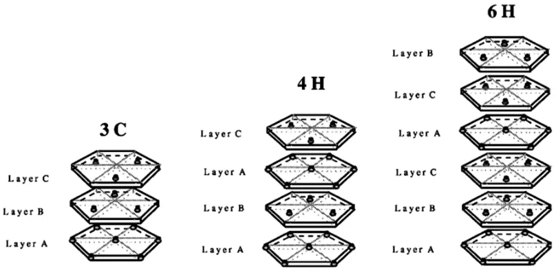
4H-SiC and 6H-SiC) are identified as most suitable substrate candidates for power devices
fabrication. The number “3” in 3C-SiC represents the three bilayer periodicity from the
stacking elements of ABC shown in Figure 2.3 and the letter “C” refers to cubic. Similarly,
and “H” refers to hexagonal.
Figure 2.2: The hexagonal packing of Si-C bilayer with three potential positions.
Table 2.1: A summary of main electrical properties of Si, GaN and SiC at 300 K [25].
Properties Units Si 3C-SiC 6H-SiC 4H-SiC GaN
Bandgap (eV) 1.12 2.4 3.0 3.2 3.4
Critical field (MV/cm) 0.25 2 2.5 2.2 3
Thermal Conduct. (W/cm.K) 1.5 3-4 3-4 3-4 1.3
Elec.Sat.Velocity (cm/s) 107 2.5×10⁷ 2×10⁷ 2×10⁷ 2.5×10⁷ Electron mobility (cm2/Vs) 1350 1000 500 950 1000
Hole mobility (cm2/Vs) 480 40 80 120 30
Int.Carrier Conc. (cm-3) ∼1010 ∼10 ∼10−5 ∼10−7 ∼10−10 Dielectric constant None 11.9 9.7 9.7 9.7 9.5
2.2
Electrical Properties
For power devices fabrication considerations, the material electrical properties such as
bandgap (blocking voltage), thermal conductivity (operation temperature), bulk carrier
mobility (resistance) and carrier saturation drift velocity (switching speed) are crucial
factors. A summary of the main electrical properties of 3C-SiC is shown in Table 2.1, in
comparison with Si and some other WBG semiconductors.
The much lower intrinsic carrier density of SiC enables devices to operate at a junction
temperature above 600◦C [26] without significant leakage currents concerns. More than
two times the thermal conductivity of Si and GaN makes sure that heat can be quickly
extracted from SiC substrates. Critical electric field of SiC is 10 times higher than Si,
with some variations depending on the polytypes. Although 3C-SiC has a narrower band
gap (2.4 eV) than 6H-SiC (3.0 eV) and 4H-SiC (3.2 eV), it has the highest bulk electron
mobility thus lower electrical resistance. Also, the unique cubic lattice provides the most
the lower electron mobility than Si, the much thinner drift region of SiC devices for a
same blocking voltage makes them much less resistive than the Si counterparts.
Figure 2.4: A general guide for the theoretical specific on-resistance of bulk Si, 3C- and 4H-SiC against the blocking voltage based on the one-dimensional unipolar
structure [27].
It is true that 3C-SiC is not as competitive as 4H-SiC in high voltage applications
targeting 10 kV and above. The device theoretical specific on-resistance is plotted in
Figure 2.4 against the blocking voltage for Si, 3C-SiC and 4H-SiC based on bulk
prop-erties. Conventional one-dimensional unipolar structures without contact corner effects
are assumed for the calculations in Figure 2.4, the depletion region width for specific-on
resistance estimation is the minimum required for the desired blocking voltage. It seems
to suggest that 4H-SiC outperforms 3C-SiC in all voltage ratings. This, however, may
region. In high voltage MOS devices design, the channel region does not contribute a
significant fraction of the total resistance compared to the thick bulk drift region. For
low and medium voltage devices, however, channel resistance becomes an important
con-tributor to the total on-resistance. Figure 2.5 (blue dashed lines) shows how the specific
on-resistance of 4H-SiC commercial devices rated below 1200 V suffer from high
chan-nel resistance, with the actual device on-resistance considerably higher than the unipolar
limit. 3C-SiC MOS devices, however, result in much lower channel resistance, and
con-sequently have some advantages in medium voltage (600-1200 V) applications. This is a
compelling advantage to fabricating 3C-SiC power devices in addition to the cost factor
mentioned before.
2.3
Challenges for 3C-SiC Grown on Si
Regardless of the best MOS interface quality among all common polytypes, 3C-SiC power
devices are not available on market mainly due to the lack of commercial 3C-SiC wafers.
Behind the attractive facade of growing 3C-SiC on Si there are a few tricky issues. 3C-SiC
can be readily heteroepitaxial grown on Si wafers back to 1984 [29], but these films suffered
from a high density of planar defects, limiting their use for power devices. Most defects
are induced by the mismatch between two semiconductors: ≈20% in lattice constant and
≈8% in coefficient of thermal expansion (CTE) [30]. A strain energy accumulates at the
3C-SiC/Si interface due to the mismatch, while forming planar defects tends to partially
release this stress. These planar defects are generally in low energy levels thus quite
stable once formed. Previous studies on 3C-SiC epitaxy layers have identified two types
of defects as most important, namely stacking faults and anti-phase domains [31, 32].
Figure 2.6: A schematic diagram of a stacking fault.
inter-rupted, such as ABC becoming ABA as seen in Figure 2.6. They act as current paths
and lead to the rise of leakage in device off-state. Theoretical calculations suggested that
the forming energy of stacking faults is negative in 3C-SiC [33], which explains why it is
so difficult to avoid them during the crystal growth stage.
Anti-phase domains are “killers” of power devices, less common than stacking faults
yet much more harmful. They are generated due to the alignment of a polar 3C-SiC
film and a non-polar Si film. In the initial growth stage, multi-nucleation of 3C-SiC
occurs since Si- and C- faces are simultaneously aligned in the [111] direction [34]. With
the growing process being carried on, nuclei with different polar face meet each other,
forming an anti-phase boundary as shown in Figure 2.7.
Figure 2.7: Schematic graph of anti-phase domains [35].
Another issue related to growing high quality 3C-SiC film on Si substrate is the
as seen in Figure 2.8, and since the 3C-SiC epilayer is usually much thinner than the Si
substrate, it is more significantly affected. This obviously does not favour devices
fabri-cation and limits the 3C-SiC film thickness because the strain increases with the epilayer
thickness.
Figure 2.8: Film bow caused by the 3C-SiC/Si interface strain and thick substrate [36].
The adoption of buffer layers is a potential solution to the interface strain. Introducing
a SiO2 layer between 3C-SiC and Si, for example, is quite effective. During the growth
process at a relative high temperature above 1000◦C, the softened SiO2 layer shares some
of the interface stress going to the 3C-SiC film. Highly oriented polycrystalline
3C-SiC(111) films grown on poly Si/SiO2/Si substrate were reported [37]. The extra poly
Si layer was deposited to achieve a better lattice match with 3C-SiC. In addition, it was
heteroepitaxy interface [38]. Schottky diodes were made on polycrystalline 3C-SiC film
grown on similar substrates (SiO2/Si) and achieved a breakdown voltage of 140 V, but
the leakage current was quite high as 1 mA/cm2 due to a high stacking faults density [39].
While being more economical and friendly to MEMS applications attributed to easily
obtained sacrificial SiO2 layers, polycrystalline 3C-SiC grown on oxidized Si or other SOI
substrates are not very effective in reducing anti-phase domains and stacking faults, thus
not great for power devices fabrications.
2.4
Chemical Vapour Deposition
Planar defects are inherently far fewer in single crystal 3C-SiC films, consequently growth
of single crystal 3C-SiC are of more interests. Variety of methods such as fast
sublima-tion [40,41] and solusublima-tion growth [42,43] were reported. Some of them obtained high quality
single crystal films with stacking faults density as low as 10-100 cm-1 [42]. Nevertheless,
none of them is able to produce large area 3C-SiC wafers suitable for industry scale
fabri-cations. As a result, although not the most convenient since usually higher temperature
and lower pressure than other methods are required, direct Chemical Vapour Deposition
(CVD) is still mostly preferred.
Figure 2.9 shows the layout of a typical induction heated horizontal CVD reactor.
Precursor gases (such as SiH4 and C3H8) are transported by the carrier gas (usually highly
on which the Si substrate wafer is loaded. Gas flow can be controlled independently by
respective controllers. Reactions between precursor gases and Si substrate go through
several stages subsequently as shown in Figure 2.10, after which a 3C-SiC layer is left
behind on the Si substrate while most H is released in the H2 form.
Figure 2.9: Illustration of the layout of a typical CVD system [22].
The specific temperature and pressure of the CVD process varies between groups for
various purposes, but typically it consists of 2 stages as shown in Figure 2.11. In the
first stage, the reactor temperature is ramped gradually to a value lower than the actual
growth temperature, and remains there for a period to carbonize the Si substrate surface.
After that, the temperature is raised again until reaching around 1400◦C, when the real
growth process kicks off.
Figure 2.11: Temperature and pressure changes during a common 3C-SiC CVD process [45].
2.5
Novel Techniques Reducing Planar Defects
The research into propagation principles of anti-phase domains and stacking faults in
with 4◦ offset towards [110] direction was found to successfully eliminate anti-phase
do-mains in epitaxy films with increasing thickness [31]. On such tilted substrates, growing
speed of domains on Si-faces are much faster than the ones on C-faces, consequently the
resulting film mainly consists of domains grown on Si-faces. However, misoriented
sub-strate was not able to reduce stacking faults, which does not only grow in a single plane. A
patterned substrate is shown by recent studies [31] to effectively reduce the stacking fault
density. More specifically, an undulant Si substrate which has counter slopes oriented in
the [110] and [-1-10] directions as shown in Figure 2.12 below.
Figure 2.12: Schematic structure of undulant Si substrate [31].
The reduction was achieved by annihilation of stacking faults originated from counter
ridges of the undulant substrate. Propagation principles of both Si-terminated stacking
faults (SFSi) and C-terminated ones (SFC) are shown in Figure 2.13 [46]. With the
vanishes in the [001] direction. SFSi, on the other hand, expands with increasing film
thickness, resulting in much lower annihilation rate. Ideally 3C-SiC should have isotropic
electrical properties since it has a cubic lattice structure, while in real cases the bulk
electron mobility of 3C-SiC film grown on Si had been found to be orientation dependent
[31]. This is most likely caused by the density difference between SFSi and SFC, which
as seen in Figure 2.13, grow perpendicularly to each other in the top view.
Figure 2.13: Propagation of both (a) Si terminated and (b) C terminated stacking fault in 3C-SiC [46].
Use of undulant Si substrate successfully reduced the stacking fault density to 5x10³ ∼
4x104cm-1range [47], still much higher than 700 cm-1, which is considered as the threshold
value for fabricating 600 V devices with leakage current below 10−4 A/cm2 [46]. The
epitaxy 3C-SiC film quality can be further improved by conducting homoepitaxial growth
on 3C-SiC substrates, namely a hetero-homo two stage process. A switch back epitaxy [32]
down, in which way SFSi were transformed into SFC so can be effectively reduced by a
follow-up homo-epitaxial growth on the back face. Selective epitaxial growth on patterned
3C-SiC substrate was also studied in [48], where sidewall patterns parallel to the (110)
face were introduced to cause some discontinuity on the 3C-SiC(001) surface, successfully
reducing the stacking fault density to less than 400 cm-1. A Monte Carlo
simulation-based comparison of above growing techniques for the stacking faults reduction is shown
in Figure 2.14, which indicates the superior performance of the two stage growing process
and the patterned 3C-SiC substrate yields the best quality epilayer. 3C-SiC on patterned
Si or SOI substrate via lateral overgrowth methods were also reported in literature [49–54],
while the quality are generally not as good as the homoepitaxy 3C-SiC films.
2.6
Physical Characterisation of 3C-SiC/Si Materials
in This Study
Despite the fact that homoepitaxy 3C-SiC film is of the finest quality for power devices
fabrication, there are currently no free-standing 3C-SiC wafers on market. In this work,
study materials are commercial 4 inch 3C-SiC(001)/Si wafers provided by NOVASiC.
Details about the growth process are kept as classified by the supplier, but generally
it follows the conventional two-stage process as described in Figure 2.11, a ∼ 1000◦C
carbonization step followed by a 1380◦C epilayer growth process. SiH4and C3H8 were used
as dual-precursor gases and diluted by highly purified H2. As-grown 3C-SiC surfaces went
through a Chemical-Mechanical Polishing (CMP) process (again NOVASiC classified) to
achieve a smooth initial surface for device fabrications. Before proceeding to any further
processing, a physical characterisation of NOVASiC materials was conducted using various
tools including X-Ray powder Diffraction (XRD), Atomic Force Microscopy (AFM) and
Transmission Electron Microscopy (TEM), and the results are summarised in following
sections.
2.6.1
X-ray powder diffraction
First of all, XRD is used to evaluate the crystal structure quality of NOVASiC wafers.
High-resolution XRD was performed using a Panalytical X’Pert Pro MRD equipped with
Pixcel detector. 2θ−Ω “powder” scans were measured between 35 and 100 2θdegrees and
the spectrum is illustrated in Figure 2.15. The only observable 3C-SiC phases are (200)
and (400), and the peaks have very small Full Width Half Maximum (FWHM) angles,
indicating the 3C-SiC film is single crystal with negligible polytype inclusions.
Figure 2.15: XRD spectrum of the NOVASiC 3C-SiC(001)/Si wafer (as-grown after CMP polishing).
2.6.2
Atomic force microscopy
The as-grown 3C-SiC surface condition is unknown since the wafers were received after
the polishing process. AFM is used to evaluate the as-polished 3C-SiC surface. A Veeco
multimode AFM with Nanonis controller was used in the contact mode with a diamond
2.16 for reference. The as-polished 3C-SiC film surface has a quite low root mean square
roughness value of 0.53 nm, an average value from five 10µm×10µm area measurements
on different locations of a 1 cm × 1 cm chip. Regardless of the potential damages left
in the surface caused by CMP, this low surface roughness value is encouraging for the
fabrication of most device features.
Figure 2.16: (a) A representative AFM figure of a 10 µm × 10µm area of the as-polished 3C-SiC surface and (b) a 3D view of the same area.
2.6.3
Transmission electron microscopy
To have a better idea of the 3C-SiC film quality, a TEM study was conducted using
JEM 2100 to check the cross section of the grown epilayer. The samples were prepared
with FIB-SEM utilising a standard lift-out technique, followed by low energy polishing.
A montage of the scanned areas from the 3C-SiC/Si interface up to the 3C-SiC surface
is shown in Figure 2.17 with enlarged views for certain regions. As can be seen, the
natural result of interface strains concentrating here. The bright voids spotted in the Si
substrate at the interface are probably a result of the Si consuming to form SiC seeds in
the initial stage of growing process. Further away from the interface, the defects density
gradually reduces, although never really vanishes even in the surface region. The stripes
which are in parallel with the Si substrate surface are stacking faults propagating in the
fashion as shown in Figure 2.13, and the inclined lines are stacking faults growing in the
other direction with the opposite termination. There are no anti-phase domains being
identified in the scanned region, which makes it promising for fabricating working devices
on these materials, even though they probably will be troubled by leakage currents due
to the considerable amount of stacking faults.
2.7
Summary
This chapter was aimed at providing the background information related to the
3C-SiC technology with an emphasis on the topics about growth and defects. The physical
characterisation of NOVASiC 3C-SiC/Si materials laid the foundation for the studies on
Chapter
3
Electrical Activation of Nitrogen
Implanted 3C-SiC(001)/Si
Firstly reported by Bernhard Gudden in 1930 [55], the unique electrical properties of
semiconductors are attributed to the impurities within their crystal lattices. It is known
that there are no chemically pure semiconductors, the frequently seen term “Intrinsic
Semiconductors” actually refers to those of negligible impurities with electrical properties
similar to insulators, which is dominated only by intrinsic carriers. In comparison,
“Ex-trinsic Semiconductors” contain considerable amount of impurities, either intentionally or
non-intentionally doped. If the impurity concentration becomes too high, the
semiconduc-tor becomes metallic. In other words, the electrical property of a semiconducsemiconduc-tor can be
modulated by controlling its impurity concentration to meet various design requirements.
As such, the study of doped semiconductor is crucial for device performance optimisation.
In this chapter, the electrical properties of implanted n-type 3C-SiC are characterised
charac-terisation tools, commonly used concepts are explained. It is then followed by a review
of previous techniques developed for SiC. Finally, a study on nitrogen heavily implanted
3C-SiC films targeting device source/drain regions is demonstrated.
3.1
Intentional Doping of the Semiconductor
Impurities are usually introduced to the semiconductor bulk in early stages of a device
fabrication process. The most commonly used dopants are group V elements (N, P, and
As) for n-type and group III elements (B, Al, and Ga) for p-type doping purposes. The
bulk doping can be relatively easily achieved by adding dopant elements into the substrate
or the epilayer growth process, and the doping level can be modulated by controlling the
precursor gases concentrations [56]. The epilayer surface is where most device features
are. Take a typical vertical MOSFET structure as an example (Figure 3.1), multiple
n-type and p-type doping regions are required for ohmic contact, MOS channel and body
diode. The selective doping area can be accurately defined by doping masks made of
dielectrics or metals using standard photolithography processes. Nowadays the selective
doping of semiconductor is achieved mostly in two ways, namely thermal diffusion and
ion implantation.
It is well-known that molecules tend to move from higher to lower concentration
re-gions, and this process can be enhanced by increasing the ambient temperature, pressure
Figure 3.1: (a) Bulk substrate, (b) epilayer and (c) selective doping of a typical vertical MOSFET.
introduce impurities using dopant sources of various phases: gas, liquid or solid. Thermal
diffusion based doping process often occurs in a quartz tube in an inert gas atmosphere to
minimise contaminations. The dopants firstly arrived at the semiconductor surface form a
relative high impurity concentration region, consequently a concentration gradient exists
between the surface and bulk, after which the diffusion is initiated by the thermal energy
provided. With the time going on, dopants diffuse deeper into the semiconductor bulk
and when the desired doping profile is obtained, the process can be stopped conveniently
by simply cutting the heat supply.
Attributed to the development of experimental physics, the ion implantation of dopants
available to device engineers [57], while now they are commonly used in both lab and
industry processing. In an ion implantation system, dopants are ionized atoms
gener-ated from an ion source as seen in Figure 3.2. Being ionized, the dopant atoms can be
accelerated by the electromagnetic field to gain a energy so high that, when hitting the
target surface, dopants are able to break the semiconductor chemical bonds and penetrate
into the crystal lattices. The implantation depth can be controlled by changing the
elec-tromagnetic field strength and the resultant impurity concentration (cm-3) is determined
by the amount of dopants supplied by the source, which is called “Dose” and usually
expressed in number per specific area (cm-2).
Figure 3.2: The schematic diagram of an ion implantation system [58].
For Si devices fabrication, both thermal diffusion and ion implantation can be used
diffusion coefficients of common dopants are negligible below 1800◦C [59], which means
thermal diffusion is not feasible thus leaving ion implantation the only option. Although a
complex and expensive system, ion implantation is more controllable than thermal
diffu-sion so that the process reproducibility is better assured. Also, the movement of dopants
in a thermal diffusion process may involve unexpected spreading in other directions,
lead-ing to poor doplead-ing profiles. This is not an issue for ion implantation since dopants
movement in the semiconductor is minimal, which means the elimination of dopants
out-diffusion. There are, of course, also limitations for ion implantations. First of all, it is
essentially a dopant bombarding process, which means damages are inevitably induced to
the target, particularly in the surface region. Secondly, as-implanted dopants are almost
always interstitial (not chemically bonded), namely not active carriers. An extra
post-implantation annealing (PIA) process is typically required to recover the lattice damage
and put the implanted dopants into substitutional positions so they can contribute to
current conduction, which is called dopants activation.
3.2
Doping Level Characterisations
During the device development stage, it is desired that the semiconductor doping level can
be measured for a better understanding of the device performance. The commonly used
evaluation tools include Capacitance-Voltage (C-V) method, Hall-effect measurements
![Figure 1.1: Expanding range of power devices applications [7].](https://thumb-us.123doks.com/thumbv2/123dok_us/9493726.455184/25.595.138.533.431.675/figure-expanding-range-power-devices-applications.webp)
![Figure 1.2: A comparison of Si, SiC, and GaN relevant material properties [8].](https://thumb-us.123doks.com/thumbv2/123dok_us/9493726.455184/26.595.145.532.178.423/figure-comparison-si-sic-gan-relevant-material-properties.webp)
![Figure 2.1: Hexagonal (a) and cubic (b) SiC lattice, dark spheres represent Si and lightones are C [22].](https://thumb-us.123doks.com/thumbv2/123dok_us/9493726.455184/32.595.112.564.154.382/figure-hexagonal-cubic-sic-lattice-spheres-represent-lightones.webp)