Vol. 31, No. 1, March, 2012, pp. 48–57. Copyrightc2012 Faculty of Engineering, University of Nigeria. ISSN 1115-8443
UTILITY INTERFACED PULSE-WIDTH MODULATION OF
SOLAR FED VOLTAGE SOURCE INVERTER USING
FIXED-BAND HYSTERESIS CURRENT CONTROLLER
METHOD
C.U. Eyaa,C.I. Odeh,D.B.N. Nnadi,M.U. Agu,S.E. Obe
Department of Electrical Engineering University of Nigeria, Nsukka, Nigeria.
a
Email: [email protected]
Abstract
This paper describes a utility interfaced pulse-width modulation of solar-fed voltage source single phase full bridge inverter. The proposed system has to do with the conversion of solar energy into electrical energy; boosting the dc power; inversion of the dc to ac and then synchronization of the inverter output with the utility, and consequently, reduction of the total harmonics distortions in the supply. The proposed system will ensure steady state availability and sufficiency of power supply to its areas of applications .To achieve this, current sensor, fixed-band hysteresis current controller and filter were employed to ensure proper injection of power to utility side and vice versa. The computer simulations and spectral analysis of the system obtained from Simplorer Software were presented. This proposed system is designed for use in residential houses and industries.
Keywords: utility interface, single phase full bridge inverter, boost converter, pulse-width modulation, fixed-band hysteresis current controller, current sensor
1. Introduction
A utility interfaced Pulse-Width Modulation of solar-fed voltage source single phase full bridge inverter with current controlled operation could be considered as the connection as well as syn-chronization of the output of single-phase full bridge pulse-width modulated (PWM) voltage source inverter (VSI) with the single phase util-ity grid system. This is achieved by sensing the current passing through the inductor so that the current and the grid voltage will be at same fre-quency and in the same phase with each other [1]. It could also be called single phase gridcon-nected pulse width modulated solar fed voltage source inverter. The inverter is to be connected between two power sources (DC and AC sources) so that whenever there is shortage of load power from photovoltaic (PV) module, it will be
sup-plemented by the utility. On the contrary, the excess power from PV module can be fed to util-ity [1]. The prime motives of the proposed sys-tem include reducing air pollution caused by the use of fossil fuel, minimization of global warming, reduction of damage to environment/ ecosystem and to respond to increase in electricity demand for the teeming population especially in Nige-ria. Even though, this proposed system suffers from minor drawbacks such as high installation costs, low conversion efficiency, variable PV out-put power and weather conditions dependent, yet it is better than total dependency on fossil fuel.
Pulse-Width Modulation Of Solar-FED Voltage Source Inverter 49
fuel globally, have prompted the development of technologies required for the use of non polluted alternative energy sources such as solar energy and wind energy [2]. It is beyond doubt that especially the high establishment of the power electronics has made the energy produced by the above alternative sources accessible and at the same time at low cost [3]. Moreover, it has al-lowed the spreading of the distributed generation (DG) consisting of a great number of small and medium generation systems connected to the dis-tribution grid to feed a dedicated consumer and then the excess to be supplied to the grid [4].
There are several ways through which power could be injected into grid utility supply that have been proposed and implemented by many people in the past. In [5] a single phase PV grid connected current source inverter topology with synchronized inverter current and voltage was presented but there was a high degree of cur-rent output fluctuations due to the losses incurred in DC link inductor used and the latching current losses of the thyristors hence reducing the effi-ciency and the power factor of the system. More-over, [6] used asymmetrical sinusoidal pulse width modulated inverter in PV grid connected system to export excess power to the grid utility. Here, there is a very wide phase shift between the fil-tered inverter current and the grid voltage in the work. So the power factor of the system is far less than unity because of the presence of unwanted signals.
The author of [7] used a resonant pulse inverter and diode rectifier coupled with PWM inverter grid-connected system in injecting power to the grid. The circuit is shown as in Fig. 1.
The circuit above consists of solar cell, the con-trolled single phase full bridge resonant pulse in-verter of high frequency carrier (input inin-verter), tank circuit, diode rectifier, and PMW current source inverter of low frequency (output inverter). It is used in injection of DC power to the grid utility from solar energy source. The PWM inverter (output inverter) synchronizes inductor current, iLF with the grid utility voltage under (k=2) discontinuous conduction mode. In this type of discontinuous conduction mode, the tank circuit rings for two complete half-cycles during each half-period of length Ts/2. After the two complete half-cycles, the rectifier diodes become
reverse-biased. The graph of output inductor current and grid utility voltage synchronization of circuit topology of Fig. 1 is shown in Fig.2. It shows that the synchronization of output in-ductor current from the PWM inverter and grid utility voltage occurs in a discontinuous current mode. In discontinuous current mode, the induc-tor current grows from the zero axes throughout the operation. The current flowing into the grid utility is more than 100 amperes with a lot of har-monic distortions contents. The Fig.3 indicates the harmonic spectral display of the inductor cur-rent of unwanted signals affecting the curcur-rent that are being injected into the utility. They contain some order of harmonics of high magnitudes; re-sulting in higher current distortions. This is be-cause at resonance state, the ringing nature of the resonating components introduces a lot of noises in the whole circuit. One of the problems of this method is that it injects high polluted currents to the grid under discontinuous conduction mode. Secondly, it is very expensive to control. And finally, the circuit is very cumbersome.
2. The Circuit Topology Of The Proposed System
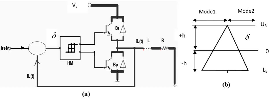
The circuit of the proposed grid-connected in-verter system of fig.4 used in the simulation con-sists of the PV cell for DC power production, the boost converter for stepping up the voltage, the insulated-gate bipolar transistors (IGBTs) and clamping diodes for conversion of DC power to AC power and for unidirectional flow of currents, reactor for filtering the unwanted signals or re-duction of the harmonic contents, and the control circuits for triggering the switches as well as en-suring the high performance and protection of the power circuit. It is worthy to note that PV used in the proposed system was under a controller called maximum power point tracker (MPPT), this will ensure that only the peak values of both current (Impp) and voltage (Vmpp) were injected into the system.
3. A Brief Concept of Hysteresis
Figure 1: Resonant-pulse – DC-link PWM inverters coupled with grid utility supply.
2!
Figure 2: Output Inductor current of Resonant /PWM inverters and the grid utility voltage synchronization.
3 4$0%1
Pulse-Width Modulation Of Solar-FED Voltage Source Inverter 51
^
ϭ^
ϰ^
ϯ^
Ϯ
^
Figure 4: The circuit diagram of the proposed Grid-connected Pulse-width modulated solar-fed voltage source inverter system.
'
()
*+
,.
/' (0%+1
(+1
(+1
G
Figure 5: Sharp hysteresis loop of a Schmitt trigger.
a system with hysteresis at an instant in time by mere taking into consideration only its input at that time. This means that its output solely de-pends on the internal state of the system and its input parameters. There are many areas where hysteresis can be applied such as in engineer-ing control, ferromagnetic materials, ferroelectric materials, elastic materials, e.t.c. For instance, Schmitt triggers are examples of electronic cir-cuits that exhibit hysteresis [2]. A sharp hystere-sis loop of a Schmitt trigger is shown in fig.5. The letters M,-M, T and -T (boundaries) are used to indicate the pathway (loop) of the hysteresis of the Schmitt trigger.
It is also used in controlling the switching mode of AC chopper for minimization of errors and fast recovery from disturbances that may exist in the system in which it is controlling.
4. The Fundamental Concepts of Hystere-sis Current Control in Voltage Source Chopper (VSC) (FEEDBACK Control)
The fundamental structure of a single-phase current hysteresis control loop of a voltage source
chopper containing R-L load, is shown in fig.5a. The load current iL(t) of the AC chopper is fed back to be compared with the reference current
iref(t) in the hysteresis modulator (HM), the cur-rent errorδ is compared with the hysteresis band as shown in fig.5b. When the current error δ
crosses the upper boundary UB, the lower chop-per switch Bp is turned ON and upchop-per chopchop-per switch Bs is turned OFF (here the delays and dead times are neglected) while the opposite pro-cess happens at the crossing of the lower bound-ary LB [2]. As a result, the output voltage is transitioned from Vssinωt to 0 and where,Vs is the input chopper voltage. The actual current is thus forced to track the sine reference wave to desired hysteresis. Another important area ap-plication of hysteresis control is in regulation of current into the grid utility supply which could be applied either in a fixed-band hysteresis current controller or sinusoidal current controller.
5. Theoretical Analysis of the Control of Current in Proposed Grid Connected PWM Voltage Source Inverter Using Fixed-Band Hysteresis Current Con-troller Approach
52 C.U. EYA, C.I. ODEH, D.B.N. NNADI, M.U. AGU, & S. E. OBE
,-,.
/' (0%+1
(+1
(+1
45
465
G
G
Figure 6: (a) Fundamental scheme of VSC hysteresis current control. (b) current error over one switching cycle.
reference current, and the error signal is passed through the hysteresis band to generate the firing signal pulses, which is operated to produce out-put voltage in manner to reduce the current er-ror signal. In fixed hysteresis band, the hysteresis bands are fixed throughout the fundamental pe-riod [8]. It gives good performance in controlling current in the course of injecting power to the grid. The algorithm for this scheme is given by the following:
iref(t) =Imaxsinωt (1)
upper band, iup = iref(t) +h
lower band, ilow = iref(t)−h (2)
Wherehis hysteresis band limit;iref is reference current; Imax is the peak current of the reference current
If iL > iup; turn OFF S1 and S2; turn ON S3 and S4
IfiL< ilow; turn OFF S3 and S4; turn ON S1 and S2
6. Maximum Switching Frequency of In-verter
The maximum switching frequency (MSF) of inverter [9] is defined as
MSF = 1
T1+T2
(Hz) (3)
WhereT1 andT2 are minimum ON and OFF pe-riods available to the device to switch from pre-vious OFF and ON states.
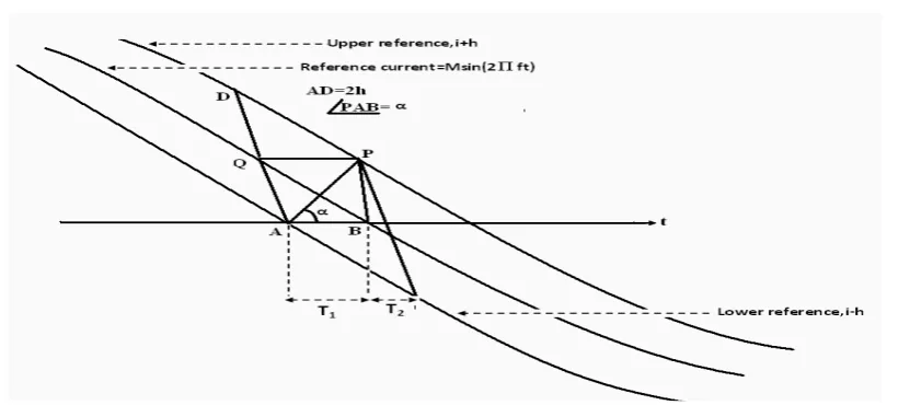
The maximum switching frequency of inverter using fixed-band current controller is analyzed considering a section drawn in Fig. 7 as shown below [8].
Considering when S1 and S2 are turned ON in Fig.7 [3], the inductor current will reach P from A in time T1 = AB. The slope of the reference current at t= T2 is expressed as:
m= di
dtt=T /2 = 2πfmM (4)
Assuming the line PD to be in parallel to the tangent drawn on the reference current at T /2 and PQ a line parallel to AB, the geometry of Fig. 7
AD = AQ+QD = 2h, with the identities of the following
AQ=P B =ABtanα=T1tanα
And QD = P Qtan(DP Q) = T1(2πfmM) T1 is approximately given by:
T1 =
2h
2πfmM+m
(sec) (5)
M = Imax = Peak value of the reference current (amps.); fm = frequency of the reference current
Pulse-Width Modulation Of Solar-FED Voltage Source Inverter 53
! "
" ! " ! " ! "
Figure 7: Determination of MSF of fixed-band Current Controller.
of the reference current( Hertz). T - fundamental period.
Then assuming that T2 = T1, the maximum switching frequency (MSF) is given by:
M SF = 2πfmM+m
4h (Hz) (6)
Considering a sampling rate of “N” per cycles, current increment of S in the sampling interval, the current slope,m, can be written as:
m= S 1/fmN
=SfmN (A/sec) (7)
The Maximum switching frequency of fixed hys-teresis band is:
(M SF)f ixed=
fm(SN+ 2πM)
4h (8)
Where N-number of sampling rate per cycle; S -current increment in the Sampling interval. The Average Switching Frequency of inverter (ASF) is defined as:
ASF = Ns
T (Hz) (9)
Where Ns - number of switching in one funda-mental period, T - fundamental period.
7. Modeling And Simulation Of Grid-Connected PWM Of Solar-Fed VSI Near Unity Power Factor
The parameters used for the simulation of the system are shown in table 1.
Table 1: Simulation parameters of utility inter-faced PWM of solar-fed voltage source Single phase full bridge inverter.
Name of the parameters Values of pa-rameters
PV module Voltage 48.00V
Frequency of Grid (Utility) 50Hz
Grid (Utility ) Voltage (220 - 230)V
Duty Cycle 0.500
Filter inductor(reactor) 0.500mH
Input Capacitor 470µF
Input Inductor 0.200mH
IGBT 6000V
Clamping diode (thermal Voltage) 32.00mV
Time duration 40ms
Carrier Frequency 20k(Hz)
Power factor got in fixed band controller 0.975
7.1. Operation of the grid-connected pulse-width modulated voltage source in-verter system
it to the inverter, where D, is the PWM duty cycle of the DC- DC converter. The inverter will still be functionless until it receives triggering signals. When it receives positive incoming signals from control unit through the gate drive terminals of the IGBT (S1, S2), it produces a gating signal to emitter voltage, VGE greater than the threshold voltage VGE(TH) to open up the IGBT channel, then the already established voltage between col-lector and the emitter, pumps the majority car-riers (electrons) from the emitter to collector ter-minals through the inversion layers which convert the available DC currents to negative half cycle of non-sinusoidal alternating current.
When the incoming terminal signal is negative to trigger gates of S3 and S4, a positive half cy-cle of non-sinusoidal alternating current appears at the collector terminals of the IGBTs; hence a complete non-sinusoidal alternating current cy-cle is formed. The continuously turning ON and OFF of the switches of the S1 and S2; with S3 and S4 produces many cycles of non-sinusoidal AC waveforms as the output of the inverter. The output of the inverter in most cases is a square wave. Then the output of the inverter is allowed to pass through an inductor which filters the rip-ples and eliminates majority of the harmonics (higher order ones) to generate a triangular- si-nusoidal waveform which is the signal output of inductor. The control unit has a feedback loop such that the switching mode is determined by comparison of the actual current and sinusoidal reference current, or the actual current oscillates in a fixed band hysteresis (FBH). This implies that the error current applied to a hysteresis el-ement, gives the PWM pattern for proper con-trolling of the injection of DC power to the grid utility.
Another function of the output inductor of 0.5mH, in Fig. 4 is that it is the point of common coupling component between the inverter and the utility grid. As soon as the output of the induc-tor is formed, the controller forces it to track the reference current in-between the upper and lower band limits accordingly in order to be delivered to the grid closed a unity power factor.
The instantaneous voltage across the inverter output for (n=1) is expressed as follow:
vinv =Vl+vgrid (10)
Vinv =
Ldil(t)
dt +V01sinωt (11)
iL(t) = 1
L
Z T
o
(vinv−V01sinωt)dt (12)
Where vin is the instantaneous inverter output voltage, L - inductance, V01 is the maximum grid voltage, ω - angular frequency, il - instan-taneous output inductor current (filtered inverter current), T - fundamental period.
8. Fixed-band Current Controller for Syn-chronization of Filtered Inverter Cur-rent and Grid Utility Voltage at near Unity Power Factor
The algorithm of the fixed-band current con-troller is stated as follows: Considering the alter-nating current from the utility supply as the ref-erence current at (n=1), that is, the fundamental component and is expressed as:
iref(t) =Imaxsinωt (13)
The upper current band of waveform is given by:
iU P =iref +h (14)
For the lower current band of the waveform, we have:
iLOW =iref −h (15)
If iL > iU P; Turn OFF S1 and S2; turn ON S3 and S4;Vinv =
−Vmpp
2
IfiL< iLOW; Turn OFF S3 and S4 ; turn ON
S1 and S2;Vinv = +V2mpp
Pulse-Width Modulation Of Solar-FED Voltage Source Inverter 55
so that the inductor current is confined within the hysteresis band limits. Under this condition the voltage output across the inverter is equal to +Vmpp/2.
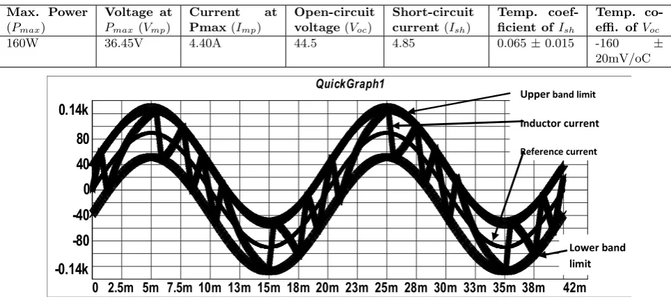
Therefore the continuously decreasing and pulling up of current gradient as the inductor cur-rent is flowing makes proper synchronization of the filtered inverter current to have the same fre-quency and in phase with the grid utility voltage. Hence, it makes the power factor of the circuit close to a unity factor. The graphical represen-tation of the fixed-band hysteresis current con-troller for controlling the injection of current into the utility grid is shown in Fig.8.
The synchronization of inverter current and grid utility voltage near a unity power factor waveforms is shown in Fig. 9. But as far as the inductor current is within the normal range, the controller continues on its normal switching oper-ation. And once it traces it well, the current flow-ing through inductor and the grid utility voltage simultaneously start from the same origin, rise at their minimum points of different amplitudes at angles of 90◦ and 270◦, fall back to zero at angles 180◦ and 360◦ to complete a cycle. Hence they are said to be synchronized and at an approxi-mately unity power factor.
Fig.4 shows the circuit representation of grid-connected PWM voltage source inverter sys-tem in which the maximum DC input power is transferred to the inverter circuit when there is uniform matching of PV impedance and the impedance of the boost converter. The input bank of capacitor bank assists in making the in-put power fluctuations ripple free.
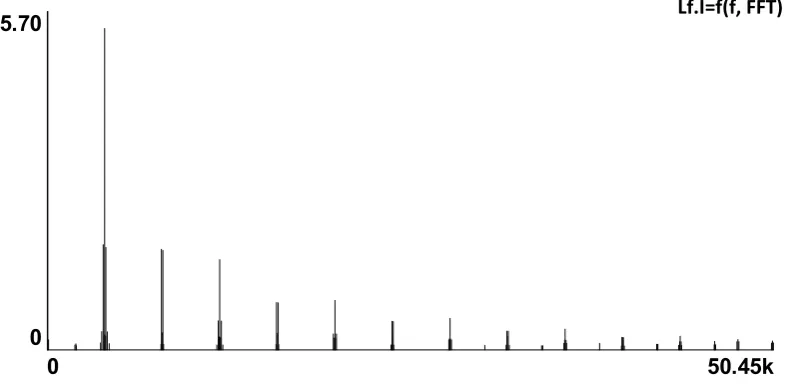
Fig.9 shows that the maximum synchronized voltage amplitude is 311(volts) and peak synchro-nized current of 98A is flowing into the grid utility near a unity power factor. The current distor-tion is drastically reduced to minimal level but not completely eliminated because of existence of irregular frequencies associated with the fixed-band hysteresis current controller on the course of regulating the flow of current into the grid. The harmonic order of the output inductor current is analyzed by Fast Fourier Transform (FFT) and is shown in Fig. 10. The total harmonic distortion is about 1.8146% and the power factor is 0.975.
9. Simulation Results
The solar module we used is BP SX 160S PV module of amorphous type. The module is made of 82 multi-crystalline silicon solar cells in series and provides 160W of nominal maximum power. Table 2 shows its electrical specification.
10. Analysis of the Results
Figures 2 and 3 show synchronization of rent and grid utility voltage and the spectral cur-rent analysis of injected curcur-rent of resonant pulse-DC-link PWM inverter coupled to the grid util-ity. The size of the amplitude current is 125A (0.125kA) and peak grid voltage is 311V. Fig.8 clearly shows the waveforms of how the output inductor current traced and tracked the reference current in the control unit of the proposed sys-tem. In Figs. 9 and 10, the synchronized filtered inverter current and utility voltage waveform and its spectral current display of the grid-connected inverter system near a unity power factor un-der fixed-band hysteresis current controller were graphically represented. The size of peak current and maximum grid voltage are 98A and 311V.
Table 3 shows clear distinctions between the two methods of injection of current into the grid utility. For instance, the peak value of current, power factor and THD in resonant pulse-DC-link PWM inverter coupled with grid utility are 125A, 0.574 and 3.061% while in the proposed system, the maximum value of current, power factor and THD are 98A, 0.975 and 1.8141%. Moreover, the size of the proposed circuit is smaller than the resonant-pulse-DC-link PWM grid connected in-verter.
Table 2: Electrical Characteristics of BP SX 160S PV Module from Manufacturer Data Sheet.
Max. Power
(Pmax)
Voltage at Pmax(Vmp)
Current at Pmax(Imp)
Open-circuit voltage(Voc)
Short-circuit current(Ish)
Temp. coef-ficient of Ish
Temp. co-effi. ofVoc
160W 36.45V 4.40A 44.5 4.85 0.065±0.015 -160 ±
20mV/oC
=9!/
3,9 !/
2!
Figure 8: Behavioral pattern of output inductor current (triangular-like waveform), reference current (ac current in middle); upper current band limit and lower current band limit at control unit using fixed- band current controller Approach or (current waveforms in hysteresis current control technique).
2!
Figure 9: The synchronized filtered inverter current (red -tooth waveform) and utility voltage waveform (dark red wave) of the grid-connected inverter system near a unity power factor under fixed-band hysteresis current controller.
3 4$0%1
Pulse-Width Modulation Of Solar-FED Voltage Source Inverter 57
Table 3: Comparison of the Resonant-Pulse DC-Link PWM Inverters coupled with Grid Utility Supply and the utility interfaced pulse-width modulation of solar-fed voltage source single phase full bridge inverter.
Name Resonant pulse-DC-link PWM
in-verter coupled with grid utility
The proposed system
Numbers of inverter used
Two inverters (input inverter of carrier fre-quency of 20kHz and output inverter of car-rier frequency of 4kHz)
One inverter of carrier fre-quency of 20kHz
Method of injected current control
Resonant method Fixed band hysteresis cur-rent approach
Size of Injected cur-rent
125A (0.125kA) 98A
Total harmonic dis-tortion(THD)(%)
3.061% 1.8141%
Power factor 0.574 0.975
Size of circuit Very large Small
Mode of current Discontinuous current mode injection Continuous current mode injection
11. Conclusion
This paper presented the utility interfaced Pulse-Width Modulation of solar-fed voltage source single phase full bridge inverter with cur-rent controlled operation at near unity power factor using fixed band hysteresis current con-troller’s approach. The simulation results have demonstrated the feasibility of the proposed sys-tem in scaled-down grid-connected condition. Moreover, due to the simplicity and fastness in the control method, low cost of production due to miniature nature of the circuit, high power factor and low cost of maintenance, the proposed sys-tem can be massively produced with little power loss in operations.
References
1. N.Mohan, T.M undeland,and W.P Robbins, Power Electronics-Converters Applications and Design, 2nd; John Wiley & Sons, Inc.1995.
2. Muhammad H.Rashid , Power Electronics-Circuits, Devices, and Applications,3rd Edition, Dorling Kindersley (India) Pvt.Ltd.2006
3. D.K Mohamed, A.Midoun, F.Safia, Optimisation of Photovoltaic generator Supplying an Induc-tion motor using fuzzy logic technique, JNVER 99 Tlemeen 1999.
4. Kjaer,S.B; Pedersen, J.K ; Blaabjer .F, A re-view of single-phase grid-connected Inverter for Photovoltaic modules,IEEE Transactions on In-dustry Applications, vol.41, no.5, pp.1292-1306, September-October, 2005
5. Calais,M; Myrzik, J. Spooner,T.Agellids,V.G, Inverters for single-phase grid-connected Photo-voltaic System-an overview, IEEE Power Elec-tronics Specialists Conference, vol.4, pp.1995-2000, 2002
6. Hassaine, E.Olias, M.Haddidi and A.Malek, Asymmetric SPWM used in inverter grid-Connected,Revue Des Energies Renouis velables vol.10 No3 (2007), pp421-429.
7. L.Malesani and D.M Divian, A Synchronized res-onant dc link converter for soft-switched PWM, in IEEE Ann. conf. Rec, 1989, pp 1037-1044.