Nigerian Journal of Technology (NIJOTECH) Vol. 31, No. 3, November, 2012, pp. 359–364. Copyright©2012 Faculty of Engineering, University of Nigeria. ISSN 1115-8443
STABILITY ANALYSIS OF A THREE-PHASE SOLID-STATE
VAR COMPENSATOR (SSVC)
A.J. Onah
Michael Okpara University of Agriculture, Umudike, Abia State, Nigeria.Email: [email protected]
Abstract
The problems associated with the flow of reactive power in transmission and distribution lines are well known. Several methods of var compensation have been applied in solving these problems. One of the modern devices employed in reactive power compensation is the three-phase solid-state var compensator (SSVC). The principal component of this device is a three-phase pulse-width-modulated voltage source inverter. A mathematical model of the inverter is derived in d-q reference frame and then used to examine the stability of the compensator in response to variations in circuit parameters.
Keywords: var compensation, inverter, stability, circuit parameters, root locus
1. Introduction
It is a well-known fact that poor power factor causes the flow of reactive power in transmission and distri-bution networks, resulting in (a) voltage drop at line ends, (b) a rise in temperature in the supply cables, producing losses of active power, (c) over-sizing of gen-eration, transmission and distribution equipment, (d) over-sizing of load protection due to harmonic cur-rents, and (e) transformer overloads.
In view of the aforementioned problems associated with poor power factor, it is necessary to improve the power factor of an installation. Before the ad-vent of modern power electronics, shunt static capaci-tors/reactors and synchronous condensers were exten-sively used to reduce the level of reactive power flowing in transmission and distribution networks [1, 2] But these elements are costly, bulky and often relatively in-efficient. As a result, extensive research developed line commutated thyristors converters in combination with some reactive components. But there is the problem of reliable controlled switching. Its effective use is only when it is force-commutated and it requires costly and complex external circuits that reduce circuit re-liability. But the advent of fast self-commutating solid-state devices (bipolar junction transistor (BJT), insulated-gate bipolar transistor (IGBT), gate-turn-off thyristor (GTO) and power MOSFET has elim-inated these problems. The voltage source inverter (VSI) employing any one of these devices is an efficient equipment for reactive power compensation or
reduc-tion of harmonic injecreduc-tion into ac mains - in order to improve power factor. They also reduce electromag-netic interference (EMI) without requiring bulky and lossy snubber circuits [3]. Equipment is available from 380V to 34.5kV.
2. The three-phase solid-state var compen-sator (SSVC)
2.1. Description
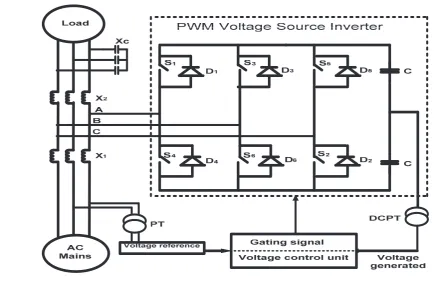
The power circuit of a three-phase solid-state var compensator (SSVC) is shown in figure 1 [4] It em-ploys a pulse-width modulated (PWM) voltage source inverter (VSI). The inverter is connected to the ac mains through a reactor X1. A dc capacitor is
con-nected to the dc side of the var compensator. The capacitor maintains a ripple-free dc voltage at the in-put of the inverter as well as storing reactive power. The SSVC is connected to the load through a second-order low-pass filter, X2 and XC, which reduces the
harmonic components of currents flowing into the util-ity grid.
2.2. Principle of operation
Figure 1: Solid-state var compensator configuration.
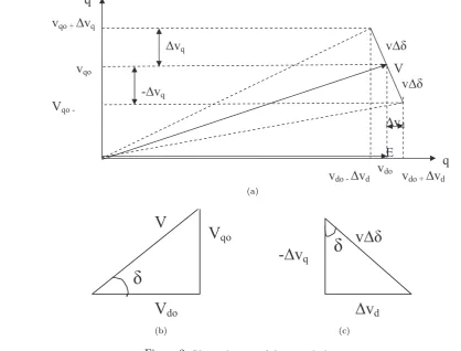
(a) Single-phase equivalent circuit.
(b) Phasor diagram.
Figure 2: V = Line-to-neutral voltage of the ac mains; E
= Fundamental component of the inverter phase-to-neutral ac voltage;i= ac current;R= Losses of the system lumped; and
L= Line inductor.
Ris negligible compared toX (2πf L) so the appar-ent power supplied by the ac source can be expressed as
S=V Ia∗=|V|∠0Ia∗
Ia∗=
|V|∠0− |E1|∠−δ
−jX
S =V
2
∠90◦−V E1∠90−δ
X
S =−V E1
X sinδ+j
V2−V E 1cosδ
X
(1)
where, δ= phase-shift angle between the source volt-age,V and the inverter ac voltage,E1.
The real power supplied by the ac source is shared by the load and the inverter. The amplitude of the fundamental component of the inverter output ac volt-age,Edepends on the value of the dc bus voltage,Vdc.
So,V increases or decreases if the capacitor is charged or discharged. The voltage drop across the inductor
X1 determines the source power factor. The voltage
drop acrossX1can be minimized by equalizingV and
Stability Analysis of a 3-Phase SSVC 361
hence maintain the source power factor at near unity. This is done by increasing the phase-shift angle,δand more active power will flow to the inverter to charge the capacitor. If the load power factor decreases, the load is taking less real power, and then the compen-sator absorbs the excess real power which charges the capacitor and then lead to higher output ofE. To re-storeEto normal value, the capacitor is discharged by decreasingδ. By controlling the phase angleδ, the dc capacitor voltage levels can be changed, and thus the amplitude of the fundamental component of the in-verter output voltageE can be controlled [5, 6]. Real power flows to the compensator if the load power fac-tor is lagging (the load is drawing less active power); and the compensator supplies real power if load power factor is leading (load requires more active power).
3. Transient Analysis of the Var Compensator
3.1. Mathematical model
From Figure 2,Ris the equivalent resistance repre-senting the total compensator system losses. To derive mathematical model of the solid-state var compen-sator, we assume that (a) the ac source is a ripple-free, balanced, three-phase voltage, (b) only fundamental components of currents and voltages are represented by the equivalent circuit, (c) since the variations in the phase-shift angle, ∆δ are small, the system is made linear [7].
From the equivalent circuit,
v(t)−e(t) =Ri(t) +Ldi(t)
dt (2)
Let δ oscillate around a mean value δo betweenδo−
∆δo andδo+ ∆δowith a frequency ωd, then,
δ(t) =δmaxcos(ωdt) =Rebδmaxejωdtc (3)
Considering the inverter voltage oscillations, the volt-ages and current can be expressed as
v(t) =V ej(ωt+∆δ) e(t) =Eej(ωt+∆δ) i(t) =Iej(ωt+∆δ)
(4)
where ω= 2πf is the ac source frequency. Ind-qaxis
v(t) = (vd+jvq)[cos(ωt+δ) +jsin(ωt+δ)]
e(t) = (ed+jeq)[cos(ωt+δ) +jsin(ωt+δ)]
i(t) = (id+jiq)[cos(ωt+δ) +jsin(ωt+δ)]
(5)
From equation (3)
v(t) =bvdcosωt−vqsinωtccos(δ)
e(t) =bedcosωt−eqsinωtccos(δ)
i(t) =bidcosωt−iqsinωtccos(δ)
(6)
Equation (5) in (2) gives
(vd−ed) cosωt−(vq−eq) sinωt=
Rid+L
did
dt −ωLiq
cosωt−
Riq+L
diq
dt +ωLid
sinωt
(7)
And then, after grouping the steady-state equations are:
vdo−edo=Rido+L
dido
dt −ωLiqo
vqo−eqo=Riqo+L
diqo
dt +ωLido
(8)
Applying small disturbances to variables in (7) around the operating point yields
vd=vdo+ ∆vd; ed =edo+ ∆ed; id=ido+ ∆id
vq =vqo+ ∆vq; eq=eqo+ ∆eq; iq =iqo+ ∆iq
(9)
Equation (7) becomes
vdo+ ∆vd−edo−∆ed=Rido+R∆id+L
dido
dt
+Ld∆id
dt −ωLiqo−ωL∆iq
vqo+ ∆vq−eqo−∆eq =Riqo+R∆iq+L
diqo
dt
+Ld∆iq
dt +ωLido+ωL∆id
(10)
Subtract (7) from (9),
∆vd−∆ed =R∆id+L
d∆id
dt −ωoL∆iq (11)
∆vq−∆eq=R∆iq+L
d∆iq
dt +ωoL∆id (12)
Multiplying equation (7) by ∆δ
vdo∆δ−edo∆δ=Rido∆δ+L
dido
dt ∆δ−ωLiqo∆δ (13)
vqo∆δ−eqo∆δ=Riqo∆δ+L
diqo
dt ∆δ+ωLido∆δ (14)
Subtract (13) from (10), and sum (11) and (12)
∆vd−∆ed−vqo∆δ+eqo∆δ=R∆id+L
d∆id
dt
−ωoL∆iq−Riqo∆δ−L
diqo
dt ∆δ−ωLido∆δ
∆vq−∆eq+vdo∆δ−edo∆δ=R∆iq+L
d∆iq
dt
+ωoL∆id+Rido∆δ+L
dido
dt ∆δ−ωLiqo∆δ
362 A.J. ONAH
/(
0&/(
0(/1
(/1
(
02/(
0 0&/(
(
00
0
(
!&/(
!(
!2/(
!/(
!(
! (a) 0 0 02 0/(
0 !& ! !1
0
!
1
(/1
/(!
&/(0
(b) 0 0 02 0/(
0 !& ! !1
0
!
1
(/1
/(!
&/(0
(c)Figure 3: Phasor diagram of the perturbed system.
Applying the Laplace transform to equation (14),
∆vd−∆ed−vqo∆δ+eqo∆δ= (R+sL)(∆id−iqo∆δ)
−ωoL(∆iq−ido∆δ)
∆vq−∆eq+vdo∆δ−edo∆δ= (R+sL)(∆iq+ido∆δ)
+ωoL(∆id−iqo∆δ)
(16)
In matrix form, the final equations for the system are
∆vd−vqo∆δ
∆vq+vdo∆δ
−
∆ed−eqo∆δ
∆eq+edo∆δ
=
R+sL −ωoL
ωoL R+sL
×
∆id−iqo∆δ
∆iq+ido∆δ
(17)
3.2. Transfer function of the compensator
Figure 3 is the phasor diagram of the perturbed sys-tem, where the inverter output voltageE is taken as the reference phasor with the ac voltage d-q compo-nents oscillating about their quiescent values,vdoand
vqowith amplitudes ∆vd and ∆vq and frequencyωd.
From figure 3
vdo=Vcos(δ)
−∆vq=V∆δcos(δ)
(18)
vqo=Vsin(δ)
−∆vd=V∆δsin(δ)
(19)
Equations (17) and (18) in (16) results in
∆vd−vqo∆δ=V∆δsin(δ)−V∆δsin(δ) = 0
∆vq−vdo∆δ=−V∆δcos(δ)−V∆δcos(δ) = 0
(20)
edo=E; ∆edo= ∆E
eqo= 0; ∆eqo= 0
(21)
If k is the modulation index of the inverter, then, the output voltage is related to the capacitor voltage as
edo=kVdco
∆ed=k∆Vdc
(22)
Equations (20) and (21) in (16) yields
∆id−iqo∆δ
∆iq−ido∆δ
=
R+sL −ωL ωL R+sL
−1
×
k∆Vdc
−k∆Vdco∆δ
(23)
∆id=
−(R+sL)k∆Vdc+ωoLkVdco∆δ
L2s2+ 2RLs+ (ω
oL)2+R2
+iqo∆δ (24)
Power balance equation of the inverter is
3
2(edid+eqiq) =VdcC dVdc
Stability Analysis of a 3-Phase SSVC 363
X)
X)
X)
X) X)
X)
Figure 4: Varying values of Capacitance,C.
Figure 5: Varying values of Inductance,L.
C is the dc capacitor. Applying small perturbations around the steady-state operating point,eq= 0,
3
2(edo+ ∆ed)(ido+ ∆id) = (Vdco+ ∆Vdc)C d
dt(Vdco+ ∆Vdc) (26) Subtracting the steady-state equation from equation (25) gives
3
2(edoido+edo∆id+ ∆edido+ ∆ed∆id−edoido) = VdcoC
d
dtVdco+VdcoC d
dt∆Vdc+ ∆VdcC d dtVdco +∆VdcC
d
dt∆Vdc−VdcoC d dtVdco
(27)
Noting that, d
dtVdco = 0, and neglecting second order
terms, (27) becomes;
3
2(edo∆id+ ∆edido) =VdcoC d
dt∆Vdc (28) ido corresponds to the steady-state current component
that provides the losses of the var compensator. Since the losses of the system are small, the product ∆edidocan
be neglected, therefore,
3
2edo∆id=VdcoC d
dt∆Vdc (29) Recall,edo=kVdco. Hence, 32kVdco∆id=VdcoCdtd∆Vdc
3
2k∆id=C d
dt∆Vdc (30) Applying Laplace transform,
3
2k∆id=Cs∆Vdc ∆id=
2Cs∆Vdc
3k
(31)
From equations (23) and (29),
∆Vdc
∆δ =
3kiqoA+ 3k2ωoLVdco
2CL2s3+ 4RCLs2+Bs+ 3k2R (32)
This is the transfer function of the var compensator sys-tem. Where, A = L2s2+ 2RLs+ωo2L2 +R2 and B =
2ω2
oL2C+ 2R2C+ 3k2L.
4. Analysis
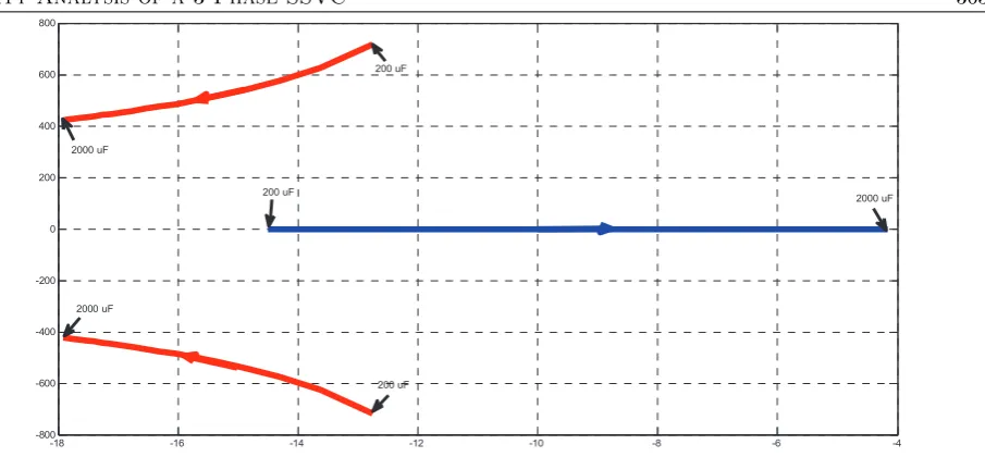
Figure 4 is the root locus of the transfer function as the value of capacitance, C varies. It can be noted that as C increases, the real negative roots (being the domi-nant poles) of the characteristic equation of the transfer function approach the imaginary axis, making the speed of system response lower, and hence the system becomes less stable [8].
The root locus of the system transfer function for in-creasing values of the inductance, L is shown in Figure 5. It is shown that the real negative roots as well as the complex-conjugate roots move towards the imaginary axis. The compensator thus takes longer time to reach steady-state and consequently is less stable.
In Figure 6 it can be seen that increasing the value of resistance, R speeds up the system response, thus enhancing stability. Ris therefore a damping component.
5. Conclusion
The features and operational principles of a var com-pensator employing PWM voltage source inverter with self-controlled dc bus, otherwise known as solid-state var compensator (SSVC) have been discussed in this paper. A model was derived, using d-q reference axis, for a var compensator operating with the δ phase-shift angle con-trol. The model has been used to investigate the system response speed and the stability of the compensator in relation to its circuit parameters. Results show that the compensator under discussion is stable for wide variations of its circuit parameters. It is shown also that, with smaller circuit parameters, the compensator reaches steady-state faster and is therefore more stable and efficient.
References
1. Juan Dixon, Luis Moran, Jose Rodriguez, Ricardo Domke. Reactive Power Compensation Technologies, State-of-the-Art Review. Electrical Engineering Department, Universidad de Concepcion, Concepcion -Chile.
2. Scott Zemerick, Powsiri Klinkhachorn, Ali Feli-achi. Design of a Microprocessor-Controlled Personal Static Var Compensator (PSVC). IEEE, 2002.
3. Shihong Park, Thomas M. Johns. Flexible dv/dt anddi/dtControl Method for Insulated Gate Power Switches. IEEE Transaction on Industry Applica-tions, Vol.39, No.3, 2003, pp. 657–664.
4. Luis T. Moran, Phoivos D. Ziogas and Geza Joos. Analysis and Design of a Three-Phase Synchronous Solid-State Var Compensator. IEEE Transactions on Industry Applications, vol. 25, No. 4, 1989, pp. 598– 607.
5. M. Benghanem, A. Tahri, A. Draou. Performance Analysis of Advanced Static Var ompensator Using Three-level Inverter. Applied Power Electronic Labo-ratory, Institute of Electrotechnics, University of Sci-ence and Technology of Oran, Algeria.
6. Guk C. Cho, Gu H. Jung, Nam S. Choi, and Gyu H. Cho. Analysis and Controller Design of Static Var Compensator Using Three-level GTO Inverter. IEEE Transactions on Power Electronics, vol. 11, No. 1, 1996, pp. 57–65.
7. Geza Joos, Luis Moran and Phoivos Ziogas. Per-formance Analysis of a PWM Inverter Var Compen-sator. IEEE Transactions on Power Electronics, Vol. 6, No. 3, 1991, pp. 380–390.