Copyright © 2013 IJECCE, All right reserved
A Proposed FPGA Based Architecture for Generation of
a Face Image
Santanu Halder
Department of CSE, Government College of Engineering & Textile Technology,Berhampore,742101, India Email: [email protected]
Abul Hasnat
Department of CSE, Government College of Engineering & Textile Technology,Berhampore,742101, India Email: [email protected]
Amina Khtaun
Department of CSE, Dumkal Polytechnic, Dumkal,West Bengal, India Email: [email protected]
Debotosh Bhattacharjee
Department of CSE,Jadavpur University, Kolkata, 700032, India Email: [email protected]
Mita Nasipuri
Department of CSE,Jadavpur University, Kolkata, 700032, India Email: [email protected]
Abstract - This paper aims to design a FPGA based architecture for generation of a new human face. This work is especially useful in criminal investigation department where a new face of a criminal is to be generated based on the description of eye-witness. Currently many image processing algorithms have been limited to software implementation which is slower due to the limited processor speed. So a dedicated processor for image processing algorithm is needed which was not possible until the advancement of VLSI technology. Now more complex system can be integrated on a single chip which provides a platform to process real time algorithm on hardware. This paper is an attempt to this direction. The FASY (FAce SYnthesis) System is a Face Database Retrieval and new Face generation System that is under development. One of its main features is the generation of the requested face when it is not found in the existing database. The new face generation system works in three steps–searching phase, assembling phase and tuning phase. In this paper the tuning phase using hardware description language and its implementation in a Field Programmable Gate Array (FPGA) device is presented.
Keywords - Face Generation Architecture, Hardware Implementation, Pipelining, VHDL, FPGA.
I. I
NTRODUCTIONThis work is a part of our main research effort to generate a new face based on the textual description from human resources when the desired face is not in the existing database [1][2]. The FASY system [1] accepts seven facial components to describe a face. The facial components are Face cutting, right eyebrow, right eye, left eyebrow, left eye, nose and lips. The Face Generation system works in 3 steps: (i) Searching phase to search the database for each single components of the face according to the user’s query. (ii) Assembling phase to place all the components at proper places to generate the full face (iii) Tuning phase to adjust the intensities to cover up the stitching lines between different pair of face components so that the generated face looks natural. This paper is focused on the VLSI realization of the last phase.
During the recent years field programmable gate arrays (FPGA’s) have become the dominant form of programmable logic [4-8]. In comparison to previous programmable devices like programmable array logic (PAL) and complex programmable logic devices
(CPLD’s), FPGA’s can implement far larger logic functions. FPGA’s supports sufficient logic to implement complete systems and sub-systems. FPGA exploit the increasing capacity of integrated circuits to provide designers with reconfigurable logic that can be programmed on application-specific basis. This drastically increases flexibility in both the design process and the final artifact by permitting one board-level design to perform many functions, or to be upgraded in the field. Here we have worked with the databases found from AT & T Laboratories Cambridge [3].
This paper is organized as follows: The section II presents the brief description of the FASY system. Section III describes the algorithm for face generation. Section IV describes the preprocessing required for hardware implementation of face generation. Section V presents the top level design of face generation hardware. Sections VI depicts the proposed system architecture for face generation. Section VII deals with the pipelining architecture introduced for the system. Section VIII describes the RTL simulation result for a set of data. Section IX shows the experimental results and finally section X concludes and remarks about some of the aspects analyzed in this paper.
II. T
HEFASY S
YSTEMFD: Face Descriptors FR: Face Retrieval FG: Face Generation PA: Parameter Adjustment
Fig.1. Block Diagram of FASY System
III.
ALGORITHM FORF
ACEG
ENERATIONThe face generation algorithm works with the neighborhood pixel values to match the intensities of the different facial components with face cutting intensities. Here 33 neighborhood intensities are considered.
Fig.2. 33 intensity matrix of face cutting for the (x, y) position
Fig.3. 33 intensity matrix of a face component for the (i, j) position
Now instead of copying the original intensities of a component onto the face cutting, we calculate a new set of intensities for each component as follows:
Suppose the intensity value of facial cutting at the position (x,y) is FI(x,y) and the intensity value of a face
component at the position (i,j) is CI(i,j) . CI(i,j) is to be
copied at the (x,y) position on the face cutting. Now instead of replacing FI(x,y)by CI(i,j), we are calculating a
new value of CI(i,j)for adjusting the intensity between face
cutting and face components.
Summation of neighborhood intensities of face cutting at point (x,y) is given by Eq.1.
FI + FI + FI + FI + FI + FI + FI + FI + FI = FI 1) + y 1, + (x y) 1, + (x 1) -y 1, + (x 1) + y (x, y) (x, 1) -y (x, 1) + y 1, -(x y) 1, -(x 1) -y 1, -(x (1) Summation of neighborhood intensities of a face component at point (i,j) is calculated using Eq. 2.
CI + CI + CI + CI + CI + CI + CI + CI + CI = CI 1) + j 1, + (i j) 1, + (i 1) -j 1, + (i 1) + j (i, j) (i, 1) -j (i, 1) + j 1, -(i j) 1, -(i 1) -j 1, -(i (2) Intensity Factor is found using Eq. 3.
CI FI =
IF (3)
Now calculate the new intensity of face cutting at the point (x,y) using Eq. 4.
IF * 2 + 1 CI * IF * 2 + FI =
FI(x,y) (x,y) (x,y) (4)
IV. P
REPROCESSING FORH
ARDWAREI
MPLEMENTATIONAs described in section II, after fetching the desired facial components from the existing database according to the textual description, user can go for the generation of the new face. Now in face generation phase, the components are placed on their proper places according to the geography of the selected blank face. Now to reduce the hardware overhead, this task is done on a rectangular black image (Fig. 4a) which has the same size as the size of the selected blank face (Fig. 4b) as shown in Fig. 4 using matlab 6.5 before feeding the image to the hardware block. The intensity value of the black region of the Fig. 4a is 0.
(a) (b)
Fig.4. A black rectangular image containing the facial components on their proper places (a) which has the same
size of (b)
Actually here the intensity values of the images are fed into the FPGA block. Now according to the method described in section III, nine pixel values are needed to calculate new pixel intensity. For this purpose, two text files have been generated for two images (the black image containing the facial components and the blank face cutting) where each file contains nine neighborhood pixel values in one line. Algorithm 1 describes the process for generating such type of file.
Algorithm 1
Algorithm Generate_Text_File(I)
//I is the image for which the intensity values are to be stored in a text file named Image.txt.
{
1. Read the image I into the variable Intensities.
2. Find the dimension of I. Suppose W stores the width and H contains the height of I.
3. Delete the file Image.txt.
Copyright © 2013 IJECCE, All right reserved 5. for i=2:H-1
6. for j=2:W-1
7. Print the value of 1,j-1), Intensities(i-1,j), Intensities(i-1,j+1), Intensities(i,j-1), Intensities(i,j), Intensities(i,j+1), Intensities(i+1,j-1), Intensities(i+1,j) and Intensities(i+1,j+1) into Image.txt.
8. Print new line (‘\n’) in Image.txt. 9. End For
10. End For
11. Close the file Image.txt. }//End of Algorithm
So, for an image with size mn, (m-2)(n-2) rows are arranged on text file. Table 1 shows the name of the text files and their purposes used for our application.
Table 1: Name of the Text files and their purposes Text file Purpose
Image1.txt Stores the intensity values of blank face. Image2.txt Stores the intensity values of black rectangular image containing the facial components in their actual position. Image3.txt Contains the intensity values of the
generated face.
V. T
OPL
EVELD
ESIGNFig.5 shows the input and output images for the FPGA module. Now according to the algorithm as described in Section III, the 9 pixel values for each of Image 1 and Image 2 are needed for calculation of the new pixel value for the output image. Again the new pixel value is calculated if and only if CI(i,j)for Image 2 is not 0. Hence the input to the face generation module is 18 eight-bit pixel values for image1, image2 and 1 eight-bit threshold value which is set to 0. The out put is 1 eight-bit pixel value generated by the algorithm described in section III. Fig. 6 shows the top level view of the face generation module.
Fig.5. The input and output images of the FPGA module
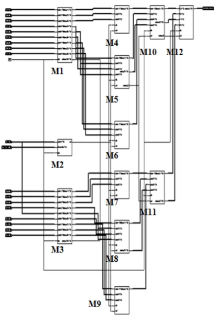
VI. S
YSTEMA
RCHITECTUREThe proposed architecture for the generation of a new face is shown in Fig. 7. The architecture contains two decoder blocks, one comparator block, four adder/divider blocks, two adder/divider/shifter blocks, two adder/divider/ shifter/sel blocks and one processing block. The modeling of the internal architecture of each block has been designed using Very high-speed integrated circuit Hardware Description Language (VHDL). Each block is controlled by a global clock.
Fig.6. Top level view of Face Generation Module
M1, M3: Decoder Block, M2: Comparator Block M4, M6, M7, M9: Adder/Divider Block
M5, M10: Adder/Divider/Shifter/Sel Block M8, M11: Adder/Divider/Shifter Block M12: Processing Block
The various blocks for this architecture are next described:
Decoder Block
The function of this block is to take nine pixel values and decode it into ten pixel values to route into other blocks. This block offers a latency of one clock cycle. The symbol of this block is shown in Fig. 8. Algorithm 2 describes the function of this module.
Algorithm 2:
Algorithm Decoder// Input: data1, data2, data3, data4, data5, data6, data7, data8, data9
// Output: dataout1, dataout2, dataout3, dataout4, dataout5, dataout6, dataout7, dataout8, dataout9, dataout10
{
dataout1 = data1; dataout2 = data2; dataout3 = data3; dataout4 = data4; dataout5 = data5; dataout6 = data6; dataout7 = data7; dataout8 = data8; dataout9 = data9; dataout10 = data5; }//End of Algorithm
Fig.8. The Symbol of Decoder Block
Comparator Block
This block generates the output 1 if the value of I25 is not 0. Otherwise it sets the output to 0. This block offers a latency of one clock cycle. The symbol of this block is shown in the Fig. 9. Algorithm 3 describes the function of this module.
Algorithm 3
Algorithm Comparator // Input: data2, threshold // Output: sel
{
If data2 > threshold then sel = 0; Else
sel = 1; End if
}//End of Algorithm
Fig.9. The Comparator Symbol
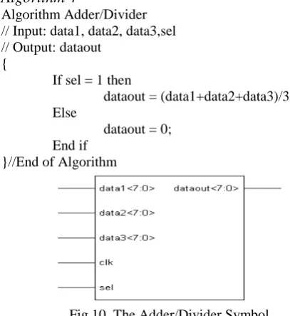
Adder/Divider Block
The function of this block is to compute the average of three pixel values coming to it if the value of the input sel is 1. If the value of sel is 0, then the output is set to 0. This block offers a latency of one clock cycle. The symbol of this block is shown in the Fig. 10. Algorithm 4 describes the function of this module.
Algorithm 4
Algorithm Adder/Divider // Input: data1, data2, data3,sel // Output: dataout
{
If sel = 1 then
dataout = (data1+data2+data3)/3; Else
dataout = 0; End if
}//End of Algorithm
Fig.10. The Adder/Divider Symbol
Adder/Divider/Shifter/Sel Block
This block computes the average of data1, data2, data3 and places the computed value to dataout1 if the value of sel is 1. If the value of sel is 0, then dataout1 is set to 0. The other functions of this block are to propagate the value of input data4 and sel to the output ports dataout2 and dataout3 respectively. This block offers a latency of one clock cycle. The symbol of this block is shown in the Fig. 11. Algorithm 5 describes the function of this module. Algorithm 5
Algorithm Adder/Divider/Shifter/Sel // Input: data1, data2, data3, data4, sel // Output: dataout1, dataout2, dataout3 {
If sel = 1 then
dataout1 = (data1+data2+data3)/3; Else
dataout1 = 0; End if
Copyright © 2013 IJECCE, All right reserved Fig.11. The Adder/Divider/Shifter/Sel Symbol
Adder/Divider/Shifter Block:
This block computes the average of data1, data2, data3 and places the computed value to dataout1 if the value of sel is 1. If the value of sel is 0, then dataout1 is set to 0. The other function of this block is to propagate the value of input data4 to the output port dataout2. This block offers a latency of one clock cycle. The symbol of this block is shown in the Fig. 12. Algorithm 6 describes the function of this module.
Algorithm 6
Algorithm Adder/Divider/Shifter // Input: data1, data2, data3, data4, sel // Output: dataout1, dataout2
{
If sel = 1 then
dataout1 = (data1+data2+data3)/3; Else
dataout1 = 0; End if
dataout2 = data4; }//End of Algorithm
Fig.12. The Adder/Divider/Shifter Symbol
Processing Block:
The function of this block is to compute the final result according to the equation 4 for the 1 value of sel. If the value of sel is 0, then this block simply propagates the value of I1 to output. This block offers a latency of one clock cycle. The symbol of processing block is shown in the Fig. 13. Algorithm 7 describes the function of this module.
Algorithm 7
Algorithm Processing // Input: CI, FI, I1, I2, sel // Output: dataout {
If sel = 1 then IF = FI/CI; dataout = (I1+2*IF*I2)/(1+2*IF);
Else
dataout = I1; End if
}//End of Algorithm
Fig.13. The Processing Block Symbol The port map of the different blocks is next reported: DECODER1: decoder
port map (clk=>CLK, data1=>I11, data2=>I12, data3=>I13, data4=>I14, data5=>I15, data6=>I16, data7=>I17, data8=>I18, data9=>I19, dataout1=>D11, dataout2=>D12, dataout3=>D13,
dataout4=>D14, dataout5=>D15, dataout6=>D16, dataout7=>D17, dataout8=>D18, dataout9=>D19, dataout10=>D110);
DECODER2: decoder
port map (clk=>CLK, data1=>I21, data2=>I22, data3=>I23, data4=>I24, data5=>I25, data6=>I26, data7=>I27, data8=>I28, data9=>I29, dataout1=>D21, dataout2=>D22, dataout3=>D23,
dataout4=>D24, dataout5=>D25, dataout6=>D26, dataout7=>D27, dataout8=>D28, dataout9=>D29, dataout10=>D210);
COMPARATOR1: comparator port map (clk=>CLK, data2=>I25, threshold=>THRESHOLD, sel=>CSEL); ADDER_DIVIDER1: adder_divider
port map (clk=>CLK, data1=>D11, data2=>D12, data3=>D13, sel=>CSEL, dataout=>AD1OUT); ADDER_DIVIDER_SHIFTER_SEL1: adder_divider_shifter_sel
port map (clk=>CLK, data1=>D14, data2=>D15, data3=>D16, data4=>D15, sel=>CSEL,
dataout1=>AD2OUT, dataout2=>ADS1OUT, dataout3 => CSEL1);
ADDER_DIVIDER2: adder_divider
port map (clk=>CLK, data1=>D17, data2=>D18, data3=>D19, sel=>CSEL, dataout=>AD3OUT); ADDER_DIVIDER3: adder_divider
port map (clk=>CLK, data1=>D21, data2=>D22, data3=>D23, sel=>CSEL, dataout=>AD4OUT); ADDER_DIVIDER_SHIFTER1:
adder_divider_shifter
port map (clk=>CLK, data1=>D24, data2=>D25, data3=>D26, data4=>D25, sel=>CSEL,
dataout1=>AD5OUT, dataout2=>ADS2OUT); ADDER_DIVIDER4 : adder_divider
port map (clk=>CLK, data1=>AD1OUT, data2=>AD2OUT, data3=>AD3OUT,
data4=>ADS1OUT, sel=>CSEL1, dataout1=>AD7OUT, dataout2=>ADS3OUT,
dataout3=>CSEL2);
ADDER_DIVIDER_SHIFTER2: adder_divider_shifter
port map (clk=>CLK, data1=>AD4OUT, data2=>AD5OUT, data3=>AD6OUT,
data4=>ADS2OUT, sel=>CSEL1, dataout1=>AD8OUT, dataout2=>ADS4OUT);
PROCESSINGMODULE1: processingmodule port map (CI=>AD7OUT, clk=>CLK, FI=>AD8OUT, I1=>ADS3OUT, I2=>ADS4OUT,
sel=>CSEL2, dataout=>DATAOUT);
VII. P
IPELININGA
RCHITECTUREPipelining is a well known technique for achieving faster clock rates while sacrificing latency. Pipeling offers an economic way to realize temporal paralallism in digital systems. To achieve pipelining one must subdivide the input process into a sequence of subtasks each of which can be executed by specialized hardware stage that operates concurrently with other stages in the pipeline. As described in the section VI, each module has a latency of one clock cycle for our application. Now module M1, module M2 and module M3 run paralally in one clock cycle. So, let us group these three modules as Stage1 (S1). Similarly, parallel modules M4, M5, M6, M7, M8 and M9 can be grouped as Stage2 (S2) which also take one clock cycle. Also modules M10 and M11 are formed Stage3 (S3) which offers one clock cycle like the previous stages. Stage4 (S4) consists of module M12. Stage4 also takes one clock cycle for execution. Fig. 14 shows the pipeline concept with four stages:
Fig.14. Concept of pipelining for face generation architecture
Fig.14 actually shows a linear pipeline that can process a sequence of subtasks with a linear precedence relation i.e. a stage Sjcan not start until all earlier stages Si( for all
i < j) finish. The space-time diagram for our system is shown in Fig. 15.
Now as described in Section IV, for an mn image total number of rows is (m-2)(n-2). Again each row takes 4 clock cycles to finish its execution. So, altogether for (m-2)
(n-2) rows total (m-2)(n-2)4 clock cycles are needed to produce the final result. But according to our design only (m-2)(n-2) + 3 clock cycles are needed for the face generation architecture described in this paper.
Fig.15. Space-time diagram of 4-stage pipeline face generation architecture
VIII. RTL S
IMULATIONSimulation for the face generation architecture described in this paper is done with the Model SimSE 6.2c. For the testing of the system correctness a testbench file is written in VHDL. The testbench file reads the data from two text files Image1.txt and Image2.txt and writes the result in a different file Image3.txt which contains the pixel values for the newly generated face. The simulation result for the testbench is shown in the Fig. 16. From the simulation result it is clear that the first output is generated after the four clock cycles of the first input set given to the system.
Fig.16. Simulation result for a set of data
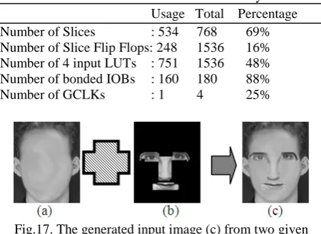
IX. R
ESULTSCopyright © 2013 IJECCE, All right reserved Table 2: Device Utilization Summary:
Usage Total Percentage
Number of Slices : 534 768 69%
Number of Slice Flip Flops: 248 1536 16% Number of 4 input LUTs : 751 1536 48% Number of bonded IOBs : 160 180 88%
Number of GCLKs : 1 4 25%
Fig.17. The generated input image (c) from two given input images (a) and (b)
X. C
ONCLUSIONThe FPGA based architecture for face generation system is proposed. This work can be especially useful for the criminal identification purpose where we have to construct a face of a criminal based on the description of eye-witness. This architecture is capable of operating at a speed of 19.860 MHz. which is much better than processing images on software platform using high level programming languages like C or C++. This frequency ensures that the result of face generation can be found out for large images like 1024 1024 pixels in just 13.13ms. Further improvement in speed could be achieved by appending more pipelining stages at different blocks.
A
CKNOWLEDGMENTAuthors are thankful to the "Center for Microprocessor Application for Training Education and Research", "Project on Storage Retrieval and Understanding of Video for Multimedia" of Computer Science & Engineering Department, Jadavpur University, for providing infrastructural facilities during progress of the work. Two of the authors, Dr. Santanu Halder and Abul Hasnat are thankful to Government College of Engineering & Textile Technology, Berhampore, West Bengal for kindly permitting him to carry on the research work.
R
EFERENCES[1] Santanu Halder, Debotosh Bhattacharjee, Mita Nasipuri, Dipak Kumar Basu, Mahantapas Kundu, “Face Synthesis (FASY) System for Generation of a Face Image from Human Description”, Third International Conference on Industrial and Information Systems, Kharagpur, INDIA December 8 -10, 2008. [2] Debotosh Bhattacharjee, Santanu Halder, Mita Nasipuri, Dipak
Kumar Basu, Mahantapas Kundu,“Construction of Human Faces from Textual Description”, Soft Computing, Springer, Vol. 15,
Issue 3, November 2009, pp. 429–447.
[3] http:// www.cl.cam.ac.UK/ Research/ DTG/ attarchive:pub/ data/att_faces.zip
[4] Michael John, and Sebastian Smith. (1997). Application Specific Integrated Circuits, Pearson Education.
[5] Jenkins, Jesse H. (1994). Designing with FPGAs and CPLDs, Prentice-Hall Publications.
[6] Weste, Neil H. and Eshraghian, Kamran (2000). Principles of CMOS VLSI Design: A Systems Perspective, Pearson Education Asia.
[7] Wakerly, John F. (2002). Digital Design: Principles and Practices, Pearson Education Asia.
[8] VHDL Programming by Example, Douglas L. Perry, Tata McGraw-Hill Edition.
A
UTHOR’SP
ROFILEDr. Santanu Halder
received the MCSE and Ph. D.(Eng.) degrees from Jadavpur University, India, in 2005 and 2012 respectively. He was associated with different institutes in various capacities until September 2009. After that he joined, Government College of Engineering & Textile Technology, Berhampore, West Bengal. His area of research pertains to the applications of Fuzzy logic, Artificial Neural Network, Genetic Algorithm, VLSI etc. in Image Processing.
Abul Hasnat
received the B. Tech degree in Computer Science & Engineering in 2005 and the M.TECH degree in Computer Science & Engineering in 2010 from West Bengal University of Technology, Kolkata. He started his professional career as lecturer in Jalpaiguri Govt. Engineering College, West Bengal in 2005. In 2008, He joined Government College of Engineering & Textile Technology, Berhampore, West Bengal. His area of interest is application of Optimization Techniques, Image processing, VLSI in different fields of Engineering.
Amina Khatun
received B. Tech degree in Computer Science & Engineering in 2011 from Govt. College of Engineering & Textile Technology, Berhampore, West Bengal and Currently she is doing M.E degree in Computer Technology in Jadavpur University, Kolkata. She is presently working as lecturer in Dumkal Polytechnic, Dumkal,West Bengal.
Dr. Debotosh Bhattacharjee
received the MCSE and Ph. D.(Eng.) degrees from Jadavpur University, India, in 1997 and 2004 respectively. He was associated with different institutes in various capacities until March 2007. After that he joined his Alma Mater, Jadavpur University. His research interests pertain to the applications of computational intelligence techniques like Fuzzy logic, Artificial Neural Network, Genetic Algorithm, Rough Set Theory, Cellular Automata etc. in Face Recognition, OCR, and Information Security. He is a life member of Indian Society for Technical Education (ISTE, New Delhi), Indian Unit for Pattern Recognition and Artificial Intelligence (IUPRAI), and member of IEEE (USA).