Design of Highly linear Gm-C Low Pass and
Complex Band Pass Filter for High Frequency
Application
WANKHADE RAHUL ONKAR
A Thesis Submitted to
Indian Institute of Technology Hyderabad In Partial Fulfillment of the Requirements for
The Degree of Master of Technology
Department of Electrical Engineering
Acknowledgements
First and foremost, I would like to sincerely thank Dr. Asudeb dutta for support as my advisor. It has truly been an honor to work with him on the very crucial Gm-C Filter Design. His strong work ethic and creative thinking is contagious to me and will influence me throughout my professional career.
Finally, I want to thank my mother, father, sister and brother. Their support is the source of power to pursue my life goal. I am eternally grateful to them.
Dedication
Abstract
The present work deals with the design of low pass filters such as 3rd order Gm-C filter, a duty cycle controlled low pass and a complex band pass filter that can be operated for high frequency appli-cations. The linearity and power consumption of a CMOS Gm-C filter are studied and optimized. Firstly, a doubly terminated 3rd order low-pass Gm-C filter is designed. The cut-off frequency is varied through capacitor and transconductance (Gm) of Operational transconductance amplifier (OTA). A high linearity is achieved by using cross-coupled differential pair OTA. The 3rd order Gm-C low-pass filter uses gyrators to implement inductor and a highly linear cross-coupled differ-ential pair OTA to implement the resistor. The power consumption is 16.44 mW with 1.8 V supply. Secondly, a duty cycle controlled reconfigurable low pass filter is designed. Variable Gm is achieved using a variable duty cycle clock pulse. Thirdly, a complex band-pass filter is designed on the basis of a low pass filter using the linear frequency transformation technique. The bandwidth, center frequency, and quality factor are made variable by using a variable duty cycle clock pulse. Low pass filter with a bandwidth of 0.3MHz to 30MHz is achieved. By using frequency transformation technique complex band pass filter with center frequency of 1.2MHz is achieved. Variable duty cycle clock pulse is obtained using the counter, an equalizer and delay flip flops.
Contents
Declaration . . . ii
Approval Sheet . . . iii
Acknowledgements . . . iv
Abstract . . . vi
1 Introduction 1 1.1 Filters and Filter theory . . . 1
1.2 Motivation . . . 2
1.2.1 MEMS resonators . . . 2
1.2.2 Simple RC filters . . . 2
1.2.3 Switched capacitor . . . 3
1.2.4 Spiral inductor-capacitor tanks . . . 3
1.2.5 Transconductance-C (or) Gm-C filter . . . 3
1.3 Major objectives of the thesis . . . 4
1.4 Thesis organization . . . 4
2 Research Background 5 2.1 Transconductance and its behavior . . . 5
2.2 Tranconductance linearization . . . 6
2.3 A Second Order Block design . . . 6
3 Design of Gm-C Low Pass Filter 8 3.1 Transfer Function of Low pass Filter . . . 8
3.1.1 Implementation of Resistor and Inductor using OTA . . . 8
3.2 Implementation of Gm-C Low Pass Filter . . . 10
3.3 Operational Transconductance amplifier (OTA) for Gm-C Low Pass Filter . . . 10
3.4 Set of Equation . . . 11
3.4.1 Common Mode Feedback . . . 12
3.5 Gm Linear Plot . . . 13
3.6 Frequency Response . . . 13
4 Duty Cycle Controlled Low Pass and Complex Band Pass Filter Design 14 4.1 Software Defined Radio Architecture . . . 14
4.2 Design of Duty Cycle Controlled Reconfigurable Low Pass and Complex Band Pass Filter . . . 15
4.2.1 Complex Band Pass Filter Implementation from Low Pass Filter . . . 15
4.2.2 Set of equation . . . 16
4.3 Digital Gates . . . 19
4.4 Outputs . . . 21
4.4.1 Frequency Response of Low Pass Filter . . . 21
4.4.2 Frequency Response of Complex Band Pass Filter . . . 21
4.4.3 5 bit counter output . . . 22
4.4.4 Variable Duty Cycle Clock Pulses . . . 24
5 Conclusion and The Future Work 26
Chapter 1
Introduction
1.1
Filters and Filter theory
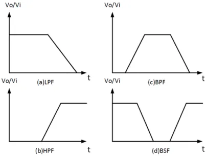
Filters are the major building block that process signals based on their frequencies. These filters are basically designed to separate signals of interest and to attenuate the unwanted noises (or) fre-quencies that are received by the receivers. These filters are used for various applications depending on the type of usage. In application like data conversion, filters are used to eliminate the effects of signal distortion in A/D systems as they are used in reconstruction of signal at the output of D/A, eliminating the high frequency components, such as its sampling frequency and its harmonics, therefore smoothing the waveform. Several hundred filters are developed for various practical appli-cations in order to meet the need of end-users. Despite several kind of filters, many of them can be explained by a few characteristics. The most important characteristic is the frequency range of the pass band. A filters pass band is the range of frequency over which an incoming signal is passed.The signal frequencies lying outside the pass band are usually attenuated. Most of the filters fall into any one of the categories based on their overall shape of pass band such as,
i) Low pass Filter which pass low frequency signals by blocking high frequency signals, where the excessive phase shift might cause oscillations;
ii) High pass filters which pass high-frequency signals by blocking DC and low frequency signals. Their pass band ranges from a corner frequency to infinity;
iii) Band pass filters which pass only the signals between two frequencies by blocking the lower and higher signals. The signals between DC and low frequencies are blocked as signals from high frequencies to infinity. The pass band of this kind of filters is characterized as having the bandwidth which is symmetric around center frequency;
iv) Band stop filters (or notch) block signals occurring between two given frequencies, FL and FH. Their pass band is split into a low-side (DC to low frequency) and a high side (High frequency to infinity).
An ideal filter will have an amplitude which is of unity for the frequencies of interest (pass band) and zero for others (stop band). The frequency at which the response changes from passband to stopband is referred as cutoff frequency. An idealized response of the most common filters are shown in Figure 1.1
Figure 1.1: Ideal Response of Common Filter
1.2
Motivation
Modern communication industries need an integrated filter design that can operate in the range of 10 to 100 megahertz and in gigahertz. Various designs of on-chip low-pass analog filters are available in recent years for band-Limiting to achieve noise reduction and also for equalizing the gain or delay. Such filters includes i) MEMS resonators, ii) Simple RC filters, iii) Switched-capacitor (SC) filters, iv) Spiral inductor-capacitor tanks and v) Transconductance-C filters. These low pass analog filters are designed for a constant delay over a wide range of frequency and also to supply gain equalization to compensate for losses in the transmission channel. The following section precisely discuss about the available filters and its limitations.
1.2.1
MEMS resonators
MEMS resonators can provide a quality factor of about 100 but requires an additional MEMS processing for its fabrication and also requires high voltage for their operation.
1.2.2
Simple RC filters
The Simple RC filters can be operated, has to undergo the variation of resistors and capacitors. Therefore each resistor has to be tuned after their fabrication. It has the limitation of operating at high frequency. The problem arises with low frequency Op amp based active RC filter is due to its integrated capacitor limitation (up to around 30pF). Frequency parameters set by RC product results in the design of large values of resistors. Larger values consume too much silicon area on circuit chip resulting in call for huge resistors design ultimately causing noise[1].
1.2.3
Switched capacitor
The SC filters can solve the variation of resistors and capacitors of simple RC filters as their filter parameters largely depend on the capacitor ratios that can be controlled in complementary metal oxide semiconductor (CMOS) processes. It is widely employed and uses RC method but avoids the usage of resistors which is hard to implement in metal oxide semiconductor (MOS) Technology with greater accuracy. It needs clock frequency generation circuits, anti-aliasing filter at the input, and smoothing filter at the output. These front-end and back-end filters are usually realized using second-order active RC filters with high tolerance polysilicon resistors and MOS capacitors. This overhead as well as the other problems mentioned regarding SC filters led to investigations on Operational Transconductance Amplifier(OTA)-C filters. However, these filters are not suitable for the frequencies greater than 10 MHz due to the requirement of unity-gain frequency of Op amp for the fast settling[2].
1.2.4
Spiral inductor-capacitor tanks
Spiral inductor - Capacitor tanks are suitable for high frequencies which lies in the GHz range. The resistance of the inductors dominates the reactance of inductance. Moreover, a lot of chip area is required for the large inductors and the large capacitors.
1.2.5
Transconductance-C (or) Gm-C filter
Gm-C can operate in a wide range of frequencies from several hundred of KHz to more than 100 MHz. It avoids operational amplifiers (Voltage-Controlled Voltage sources) and obtains the gain from transconductance amplifiers (Iout = gm Vin). The design of gm-C filters uses only transconductance amplifiers and capacitors which is why the name is termed as the transconductance-C (or Gm-C). Frequency parameters are set by gm/C ratios which makes transconductance value even at smaller level readily obtained with normal processing and biasing. The limit of the operation frequency of these filters is the amount of excess phase which depends on the speed of response of the filters. Unlike the spiral inductors, the quality factor of gm-C filters can be adjusted by controlling the output impedance even at lower frequencies[2]. Band pass filters are commonly used in (wireless) transmitters and receivers. The main function of this filter in transmitters is to limit the bandwidth of the output signal to band allocated for transmission. A band pass filter allows signals within a selected range of frequencies to be heard or decoded in receivers, by preventing signals at unwanted frequencies. A band pass filter can also optimize the signal-to-noise ratio and sensitivity of the receiver. An ideal band pass filter will have a completely flat pass band with no gain or attenuation throughout and will completely attenuate all frequencies outside the passband. It is impossible to have an ideal band pass filter in practice. In real, the filter does not completely attenuate all frequencies which is not desired. There is a filter roll-off expressed in dB per octave or decade of frequencies known to be attenuated than being rejected. In the design, the roll-off is made as narrow as to allow the filter to perform as nearly as its intended design. This is achieved at the expense of pass band or stop band. A band pass filter can be characterized by Q factor. It is the inverse of the fractional bandwidth. A high Q filter will have narrow pass band and a low Q filter will have wide pass band. The present work deals with the design of a low pass filters (Gm-C based) and a complex band pass filter based on a low pass filter which can be operated for high frequency applications.
1.3
Major objectives of the thesis
Main objective of the thesis is to design the Gm-C low pass filter and complex band pass filter for high frequency application. Our aim is to design highly linear OTA. The aim of the design is to achieve variable bandwidth using transconductance and capacitor.
1.4
Thesis organization
The detail of the work is put in the chapters as shown below which is explained completely in later stages.
Chapter 1 : In this chapter introduction describing the motivation behind the work, literature survey, objectives and contributions of the present work.
Chapter 2 : Describes basics of implementation of the second order gm-c biquad filter.
chapter 3 : Design of 3rd order low pass Gm-C filter.
Chapter 4 : Design of Duty cycle controlled clock pulse low pass and complex band pass filter.
Chapter 2
Research Background
2.1
Transconductance and its behavior
The transconductance is the most important building blocks in analog and mixed mode circuits which includes multipliers [3 and 4], continuous-time gm-C filters [5 and 6], voltage controlled oscillators and continuous-time sigma-delta modulators. In order to understand the behavior of transconductance cell, it is essential to find the transconductance parameters of the model. The model is restricted to MOS technology in which the analog integrated filters should be able to reside together with digital circuits on the same integrated circuit. In saturation region, MOS transistor is governed by the following equation (2.1)
ID=
1
2unCox(VGS−Vth)
2 (2.1)
The models output current is the total drain current
io=iD (2.2)
The dc bias current ID and the ac current iD(t) Total current is
io=ID+iD(t) (2.3)
The input voltage
v1=VGS+Vgs(t) (2.4)
is the total gate to source voltage, is the carrier mobility, Cox is the oxide capacitance per unit area of the channel which will have typical value 1.5 F/ m2 and Vt is the threshold voltage. gm can be adjusted by the width-to-length ratio, W/L, and is proportional to the square root of the bias current ID.
2.2
Tranconductance linearization
The main idea is to convert the input voltage into output current with a linear transformation factor. The passive devices are replaced by active devices that owes to power and area consideration with high tradeoff of non-ideal performance of system. The foremost non-ideal characteristics of the transconductor are the limited linear input range, limited output impedance, finite bandwidth and finite signal-to-noise ratio. The linear performance is of great issue in the design of transconductance cell. As the feature size of CMOS technology scales down along with supply voltage, bandwidth, the dynamic range, and power consumption will be limited under specific linearity. There are many techniques implemented to reduce the variation of gm of differential pairs towards the variation of Vid. These technique includes i.) Source degeneration, ii.) 2. Cross-coupling. iii.) Compensation using unbalanced differential pairs and iv.) Active biasing.
2.3
A Second Order Block design
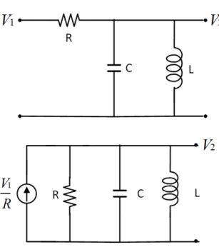
Figure 2.1: Passive RLC circuit
The present study deals with the second order block design as it starts from the passive RLC circuit shown in Figure 2.1. The transconductance C implementation is recognized as shown in Figure2.2. The present study deals with second order block design as it starts from the passive RLC circuit and a source transformation was performed to get circuit as shown in Figure 2.1. The transconductance C implementation is recognized as shown in Figure 2.2
V0is obtained from V2by integration Eq(2.4), At V0 we have low pass output. The differential
version of Low pass filter is shown in Figure 2.2. Which is obtained from Figure 2.1. Gm1converts
the input voltage to a current, Gm2 represents resistor R, the capacitor C1 is unchanged and Gm3
and Gm4 form a gyrator, which together with the capacitor C2 implements the inductor L = C2 /
(Gm3Gm4).The circuit can then be analyzed and for simplicity we use the one to one correspondence with the passive prototype (Eq 2.1), and obtain the transfer function of low pass filter as given in
Figure 2.2: Second Order Biquad Filter
the set of equations.
V2 V1 = G G+sC1+ 1 sL (2.5) V2 V1 = gm1 gm2 +sC1+ gm3gm4 sC1 (2.6) V o= gm3V2 sC2 (2.7) V0 V1 =gm3V2 sC2V1 (2.8) V0 V1 = gm1gm3 s2C 1C1+sC2gm+gm3gm4 (2.9)
Chapter 3
Design of Gm-C Low Pass Filter
3.1
Transfer Function of Low pass Filter
T(s) = 2Gm2 s3CLC1C2 GmL2 + s2CL(C1+C2) GmL2 + s(C1+C2)CL GmL2 + 2G (3.1) R= 1/G= 1/Gm1 (3.2)
Figure 3.1: Design of the low pass passive prototype 3rd order low pass filter
3.1.1
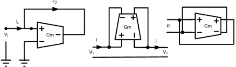
Implementation of Resistor and Inductor using OTA
Figure 3.2: Implementation of Resistor using OTA Grounded resistor,Floating Resistor and Differ-ential
ID=
1
2k(VGS−Vth)
Figure 3.3: Implementation of Inductor using Gyrator
Figure 3.4: A Floating inductor realized using capacitor embedded between two gyrator
3.2
Implementation of Gm-C Low Pass Filter
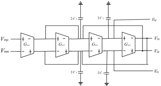
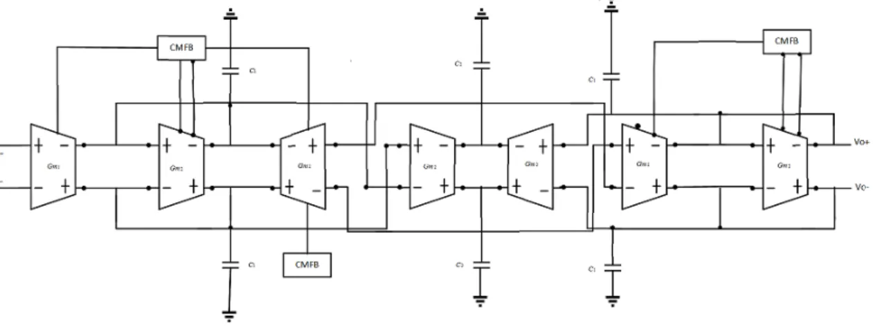
Common-mode feedback (CMFB) circuits are required to stabilize common-mode voltages. The CMFB used has an advantage of inherent common-mode voltage available in the OTA, where the source degeneration resistors in the OTA act also as a common-mode detector [7] Thus, for two OTAs connected in cascade, the detected in the second OTA is used to control the common-mode voltage of the first OTA through (gate voltage of M4) in the first OTA. It is implemented with seven OTAs and three common-mode feedback circuits, as shown in Figure 3.6. Most of the OTAs have a similar transconductance value for this implementation, but the input OTAs transconductance is about twice that of the rest of the OTAs to keep a unity dc gain of the filter[8].
Figure 3.6: Block Diagram for the implementation of Gm-C Low Pass Filter.
3.3
Operational Transconductance amplifier (OTA) for
Gm-C Low Pass Filter
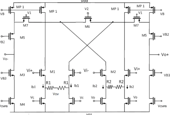
Active-RC filters have very high linearity and low-noise performances. However, they consume high power and large silicon area and are only suitable for modest operating frequencies (10 MHz). This is because high loop gain at high frequencies requires opamps with very large gain bandwidth product. Transconductance-C ( Gm-C) filters, on the other hand, have relative lower power consumption and small areas and are suitable for high-frequency operation, but high linearity is hard to achieve because they operate in open-loop. Continual efforts have been made to improve the linearity of Gm-C filters. The cross-coupled differential pairs with source degeneration shown in Figure 3.6 have been used to achieve high linearity and high-frequency operation. For this OTA structure, all transistors operate in the saturation region. The drain current of a MOS transistor is approximated as shown in equation 3.4. Source degeneration resistors R1=R2=0, the low-frequency differential output current of a differential pair is given in the equation (3.6) and expanding the equation 2 in a Taylor series and considering only the first terms, we will get equation (3.7). The analysis can be extended to the case of two cross-coupled differential pair, the differential output current (with R1=R2=0) becomes as shown in equation (3.8). On adding the source degeneration resistors R1,R2 and mobility degradation effects R1, R 2 as shown in literature [9], it can be shown that the
differential output current can be approximated as expressed in equation (3.8). The low frequency Small- transconductance Gm for the coupled differential pairs with source degeneration yield is shown in equation (3.9). To provide independent transconductance control while maintaining good linearity, a current division approach is used as described in [10] and [11]. The bias tail currents Ib1 and Ib2 are fixed and optimized for best linearity and the current. Division factor adjusts the
OTA’s transconductance. The division factor a is given by = (rml/2)/((rml/2)+rm2) where rml and rm2 are the resistance values of the triode region operating transistors[10] . The factor a can be controlled adjusting the voltages V1 and V2.
Figure 3.7: Cross Coupled Differential with Source Degeneration OTA
3.4
Set of Equation
ID= 1 2k(VGS−Vth) 2 (3.4) iod= p 2kIDvd s 1− vd 2Vdsat 2 =gmvd s 1− v d 2Vdsat 2 (3.5)iod= p 2kIDvd s 1− vd 2Vdsat 2 =gmvd s 1− v d 2Vdsat 2 (3.6) iod=gmvd− gm 8V2 dsat vd3 (3.7) iout= g m1 1 +Nr1 − gm2 1 +Nr2 vd −1 8 gm1 V2 dsat1(1 +Nr1)3 − gm2 V2 dsat2(1 +Nr2)3 vd3 (3.8) Gm= gm1 1 +Nr1 − gm2 1 +Nr2 HD3= v2d−pk 32 gm1 V2 dsat1(1+Nr1)3 − gm2 V2 dsat2(1+Nr2)3 gm1 1+Nr1 − gm2 1+Nr2 (3.9)
In the above equations, ID is the drain current, VGS is the gate to source voltage, Vth is the
threshold voltage, and k is the transconductance parameter. Vd is the differential input voltage.
3.4.1
Common Mode Feedback
3.5
Gm Linear Plot
Figure 3.9: Gm linear plot
3.6
Frequency Response
Figure 3.10: Frequency Response of Low Pass Filter with cut off frequency 12MHz,17MHz and 32MHz with variable capacitor
Table 3.1: PERFORMANCE OF THE FILTER Parameter Value Technology UMC 180nm Supply Voltage 1.8 V
Filter Type 3rd order Cut Off Frequency 12M-32MHz Power consumption(OTA) 16.44mW Power consumption of filter 15.876mW
CMRR 55dB
Chapter 4
Duty Cycle Controlled Low Pass
and Complex Band Pass Filter
Design
4.1
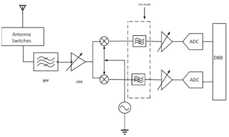
Software Defined Radio Architecture
The Software defined radio (SDR) receiver architecture with tunable function block is shown in Figure 4.1. The signal received through an antenna interface is amplified by a low-noise amplifier (LNA) and is directly down-converted to the baseband or IF by a quadrature mixer. The following analog filter attenuates adjacent interferers and the programmable gain amplifier (PGA) controls a signal level for the ADC with a limited dynamic range[12].
4.2
Design of Duty Cycle Controlled Reconfigurable Low
Pass and Complex Band Pass Filter
The filter control pulses are produced by a variable duty-cycle pulse generator, which basically oper-ates as a frequency divider, with small overhead in area and power. The design is carried out in three steps. First a low-pass ladder prototype is represented. Then, replacing the inductors and resistors in the prototype with transconductors and capacitors, a fully-balanced low-pass filter containing only transconductors and capacitors is derived. Finally, using linear frequency transformation as shown in Fig.4.3 by transconductor pairs, the desired complex filter is derived from the low-pass filter. We replace the inductor L and resistor R in the prototype with transconductors and capacitors to get an active low-pass filter It can be calculated that the equivalent value of the differential inductor. We use frequency transformation to derive the structure of a complex band-pass filter based on Gm-C technique.
Wo=
GmLH
C (4.1)
4.2.1
Complex Band Pass Filter Implementation from Low Pass Filter
Figure 4.2: Linear Frequency Transformation
Figure 4.4: Inverter based Gm block
Figure 4.5: Transmission Gate
4.2.2
Set of equation
phi(t) = 1, 0≤t≤TON 0, otherwise (4.2) Qsig= (n+1)TCLK Z nTCLK Gm0vin(τ)dx =e jωTON−1 jωTCLK ejω(nTCLK−t)Gm0 (4.3) Gmeff = i sig vin =e jωTON−1 jωTCLK ejω(nTCLK−t)Gm0 (4.4) v2 th= 4kT γ Gm0 ∆f (4.5) T(s) =− Gm1Gm2 C1C2 s2+Gm3 C1 s+ Gm2Gm4 C1C2 . (4.6) ωc= r Gm2Gm4 C1C2 (4.7)Q= √ Gm2Gm4 Gm3 r C1 C2 (4.8)
Unity gain frequency depends upon transconductance of the amplifier and load capacitor. Load capacitor = 1pF . If unity gain frequency is getting varied then we can say transconductance of the amplifier is getting varied. Gm0=296u
Figure 4.6: Variable Transconductance using duty cycle control (Gm0=296u ,load=1pF)
Figure 4.7: Variable Transconductance concept using Duty Cycle Clock Pulse
The DT LPFs are designed based on a second-order filter with independently controlled transcon-ductors, where the filter characteristics can be tuned by only changing the duty cycle of the control pulses. A concept of the proposed transconductor is shown in Fig. 4.6. The DT transconductor consists of a transconductor core and two switches. A single-ended version is depicted for simplicity. The switching of SW1 and SW2 is controlled by a clock pulse 1 and its inverse , respectively. The waveforms of the input voltage and the output current are also shown in Fig.4.6 as an example, When is high-level and SW1 is on-state, the output current of the transconductor core is fed into
the following stage. When 1 becomes low-level and SW1 is off-state, SW2 turns on and the output current of the transconductor core flows to the ground[13]. The clock pulse 1 be equation (4.2) of inverter based gm where is a hypothetical complex sinusoid of frequency as an input voltage signal. The transconductance gain of the DT transconductor is time variant. It is Gmo when 1 is high-level, and zero otherwise, where Gmo is the transconductance gain of the core. Then, the signal charge transferred to the following stage during n-th sampling period can be expressed as in equation (4.3). Where Vin (t) is a hypothetical complex sinusoid of frequency as an input voltage signal[12]. By using the time-averaged signal current, a time-averaged effective transconductance gain becomes as expressed in Equation(4.4). Under the condition that the input frequency is low enough compared to the clock frequency, (4.3) can be approximated as expressed in equation (4.4) Equation (4.4) denotes that can be controlled by the ratio of TON to TCLK, that is the duty-cycle of the clock
pulse. Since the DT transconductor operates like a switching mixer, noise folding will occur; the wideband noises, such as a thermal noise, are mixed by the sampling clock and down-converted to the baseband. As for flicker noise, which contributes in a low frequency, it does not experience noise folding. It does not depend on the duty-cycle too. Furthermore, the flicker noise level itself is low, because a large-sized transconductor core can be used even if a small transconductance gain is required in a narrow bandwidth filter mode[13]. Thus, only thermal noise is analyzed here. Provided that the input-referred thermal noise voltage of the transconductor core in the frequency range f is expressed in equation (4.5).
Figure 4.9: Design of Variable Duty Cycle Generator
Figure 4.10: 5-Bit Counter
4.3
Digital Gates
Figure 4.12: NOR GATE
Figure 4.13: XOR GATE
Figure 4.14: D FF
4.4
Outputs
4.4.1
Frequency Response of Low Pass Filter
Figure 4.16: Frequency Response of Low Pass Filter with Cut off Frequency .35M-51MHZ
4.4.2
Frequency Response of Complex Band Pass Filter
Figure 4.17: Frequency Response of Complex Band Pass Filter with Center Frequency of 1.2MHz and Bandwidth .6M-1.2MHz
4.4.3
5 bit counter output
Figure 4.18: MSB of counter
Figure 4.20: counter output
Figure 4.21: counter output
4.4.4
Variable Duty Cycle Clock Pulses
Figure 4.23: Variable Duty Cycle
Figure 4.25: Variable Duty Cycle
Table 4.1: PERFORMANCE OF THE FILTER Parameter Value
Technology UMC 180nm Supply Voltage 1.8 V
Filter Type 4th order Cut Off Frequency .35MHz-51.16MHz
Center Frequency 1.2MHz Bandwidth .6MHz-1.2MHz
Chapter 5
Conclusion and The Future Work
Gm-C filters are capable of operating at high frequency. However, designing operational transcon-ductance amplifier is challenging. In this research, design of Gm-C low pass filter , duty cycle controlled low pass filter and complex band pass filter design. In order to optimize the performance of the Gm-C filter, linearization techniques are investigated and proposed. Another shortcoming of Gm-C filters is the wide variation of center frequency and Q due to process variations. This requires the Gm-C filter to be tunable over a wide range. The Gm-C low pass filter is designed with cross coupled differential pair OTA. The 4th order duty cycle controlled Gm-C low pass filter and complex band pass filter is designed .The transconductance is designed using Inverter.Designing Gm was challenging by using duty cycle control clock pulse. Variable duty cycle clock pulse was achieved using counter, equalizer, delay FF.
As linearity of OTA is very important parameter while designing of the filter in low power, so there is lot of scope to design low power highly linear OTA. Different methods are possible to tune the cut off frequency of the filter.
Chapter 6
Bibilography
1) Rolf Schaumann and Mac E. Van Valkenburg.Design of Analog Filters, Jan 15, 2001
2) Lo, Tien-Yu, Hung, Chung-Chih (Frank) 1V CMOS Gm-C Filters Design and Applications
3) M. Ismail and T. Fiez, Analog VLSI Signal and Information Processing. New York: Mc-GrawHill, 1994.
4) S. R. Zarabadi, M. Ismail, and C. C. Hung, High performance analog VLSI computational circuits, IEEE Journal of Solid-State Circuits, vol. 33, no. 4, pp. 644649, Apr. 1998.
5) T. Y. Lo, C. C. Hung, and M. Ismail, A wide tuning range Gm-C filter for multimode directconversion wireless receivers, Proc. IEEE Eur. Solid-State Circuits Conf., pp. 210213, 2001.
6) T. Y. Lo and C. C. Hung, A wide tuning range Gm-C continuous-time analog filter, IEEE Trans. Circuits Syst. I, Reg. Papers., vol. 54, no. 4, pp. 713722, Apr. 2007.
7) Silva-Martinez, J.; Adut, J.; Rocha-Perez, J.M.; Robinson, M.; Rokhsaz, S., ”A 60-mW 200-MHz continuous-time seventh-order linear phase filter with on-chip automatic tuning system,” Solid-State Circuits, IEEE Journal of , vol.38, no.2, pp.216,225, Feb 2003
8) Jianlong Chen; Sanchez-Sinencio, E.; Silva-Martinez, J., ”Frequency-dependent harmonic-distortion analysis of a linearized cross-coupled CMOS OTA and its application to OTA-C filters,” Circuits and Systems I: Regular Papers, IEEE Transactions on , vol.53, no.3, pp.499,510, March 2006
9) P. R. Gray, P. J. Hurst, S. H. Lewis, and R. G. Meyer, Analysis and Design of Analog Integrated Circuits 2001, Wiley
10) Bult, K.; Geelen, G.J.G.M., ”An inherently linear and compact MOST-only current divi-sion technique,” Solid-State Circuits, IEEE Journal of , vol.27, no.12, pp.1730,1735, Dec 1992
11) Mensink, C.H.J.; Nauta, B., ”CMOS tunable linear current divider,” Electronics Letters , vol.32, no.10, pp.889,890, 9 May 1996
12) Kitsunezuka, M.; Tokairin, T.; Tadashi Maeda; Fukaishi, M., ”A Low-IF/Zero-IF Recon-figurable Analog Baseband IC With an I/Q Imbalance Cancellation Scheme,” Solid-State Circuits, IEEE Journal of , vol.46, no.3, pp.572,582, March 2011
13) Kitsunezuka, M.; Hori, S.; Tadashi Maeda, ”A Widely-Tunable, Reconfigurable CMOS Analog Baseband IC for Software-Defined Radio,” Solid-State Circuits, IEEE Journal of , vol.44, no.9, pp.2496,2502, Sept. 2009
14) Behzad Razavi Design of Analog CMOS Integrated Circuits McGraw Hill Education,2000
15) Phillip E. Allen CMOS Analog Circuit Design:2nd Edition, 2002
16) Sansen, Willy M. C. Analog Design Essential Springer,2006
17) Artur Lewinski and Jose Silva-Martinez OTA Linearity enhancement technique for high frequency applications with IM3 below -65dB
18) MOS Transconductance AND integrator with high linearity electronics letters Vol.N0.5
19) Chang, Z.Y.; Haspeslagh, D.; Boxho, J.; Macq, D., ”A highly linear CMOS Gm-C band-pass filter for video applications,” Custom Integrated Circuits Conference, 1996., Proceedings of the IEEE 1996 , vol., no., pp.89,92, 5-8 May 1996
20) S. Koziel and S. Szczepanski, ”Design of highly linear tunable CMOS OTA for continuous-time filters” IEEE Trans. Circuits Syst. II, vol. 49, no. 2, pp. 110-122, 2002