ISSN(Online): 2319-8753 ISSN (Print): 2347-6710
I
nternational
J
ournal of
I
nnovative
R
esearch in
S
cience,
E
ngineering and
T
echnology
(A High Impact Factor, Monthly, Peer Reviewed Journal) Visit: www.ijirset.com
Vol. 8, Issue 8, August 2019
Design and Analysis of SRAM Cells in Ultra
Deep Submicron CMOS Technology
Sitaram Chowdhary, Dr. Surendra Bohra
Research Scholar M. Tech. (VLSI), SLBS Engineering College, Jodhpur, India Professor & Principal, SLBS Engineering College, Jodhpur, India
ABSTRACT : Since short-circuits are responsible for much of the dynamic power loss, concept of virtual source transistors is used for removing direct connection between VDD and GND. Faster write time can be achieved by using transmission gates
instead of simple NMOS pass transistors. By implementing these improvements seven different memory cell designs are proposed. Each of these designs has been extensively simulated in 16nm CMOS predictive technology for comparison with the standard six-transistor (6T) differential memory cell. Simulation results indicate similar type of outputs for same input while working with these designs but power dissipation and delay has significant changes with varying schemes.
Secondly the technology is also scaled down to 16nm so power and speed is also optimized accordingly for future scope of designing. Besides these factors, very small device dimensions show a remarkable area reduction, which is also an added advantage. As size is a prime concern for SRAM cell as well as for all SOCs, in which memory occupies more than 50% of space.
I. INTRODUCTION
The increasing market of mobile, hand-held devices and battery powered portable electronic systems as well as the increase in data transfer rates demands that these systems use less power and reduce operational delays. These devices and systems demand high-speed, high-throughput computations, complex functionalities and often real time processing capabilities. The performance of these devices is limited by the size, weight and lifetime of batteries. Serious reliability problems, increased design costs and battery operated applications prompted the IC design community to look more aggressively for new approaches and methodologies that produce more power efficient designs, which means significant reductions in power consumption for the same level of performance. For five decades, the semiconductor industry has distinguished itself by the rapid pace of improvement in its products. The principal categories of improvement trends are shown in Table 1.1 with examples of each. Most of these trends have resulted principally from the industry’s ability to exponentially decrease the minimum feature sizes used to fabricate integrated circuits. Of course, the most frequently cited trend is in integration level, which is usually expressed as Moore’s Law (that is, the number of components per chip doubles roughly every 18 months). The most significant trend is the decreasing cost per function, which has led to significant improvements in economic productivity and overall quality of life through proliferation of computers, communication, and other industrial and consumer electronics.
Table 1: Improvement Trends for ICs Enabled by Feature Scaling
TREND EXAMPLE
Integration Level Components/chip, Moore’s Law Cost Cost per function
ISSN(Online): 2319-8753 ISSN (Print): 2347-6710
I
nternational
J
ournal of
I
nnovative
R
esearch in
S
cience,
E
ngineering and
T
echnology
(A High Impact Factor, Monthly, Peer Reviewed Journal) Visit: www.ijirset.com
Vol. 8, Issue 8, August 2019
Since memory currently makes up a large part of systems, nearly fifty percent, reducing the power and delay in memories becomes an important issue. In fact, some systems, such as the reconfigurable hardware which uses the memory latch as its most basic component, have an even larger percentage of their structure built with memory. Memories are also responsible for almost half of the total CPU dissipation.
II. BASICS OF SRAM CELLS
Static Random Access Memories (SRAMs) are used extensively in all kinds of systems and are found in almost every integrated circuit as an embedded component. They are known for their large storage density and small access latency.
Properties of SRAM
An SRAM cell offers the following basic properties:
• SRAM is a form of random access memory: A random access memory is one in which the locations in the semiconductor memory can be written to or read from in any order, regardless of the last memory location that was accessed
• Retention: An SRAM cell is able to retain the data indefinitely as long as it is powered.
• Read: An SRAM cell is able to communicate its data. This operation does not affect the data i.e., Read operation is non-destructive.
• Write: The data of an SRAM cell can be set to any binary value regardless of its original data.
• SRAM Architecture
Memory cells are the key components of any SRAM serving for storage of binary information. A typical SRAM cell is comprised two cross-coupled inverters forming a latch and access transistors. Different types of SRAM cells are based on the type of load used in the elementary inverter of the flip-flop cell. Access transistors enable read and write access to the cell and cell isolation for the not-accessed state. An SRAM cell has to provide non-destructive read access, write capability and infinite storage (or data retention) time provided the power is supplied to the cell. Hierarchically, memory cells are arranged in cores, which can be further divided into blocks and arrays depending on the system speed and power requirements.
We will consider three of the more recent SRAM cells: a resistive load four-transistor (4T) SRAM cell, a loadless 4T SRAM cell and a six transistor (6T) CMOS SRAM cell. We will then discuss their advantages and disadvantages. The cell design considerations represent a tradeoff between cell area, robustness, speed and power. Cell size minimization is one of the most important design objectives. A smaller cell allows the number of bits per unit area to be increased and thus, decreases cost per bit. Reduced cell size can indirectly improve the speed and power consumption due to the reduction of the associated capacitances. However, the cell area might have to be traded off for high performance or low power, radiation hardness or special functionality requirements.
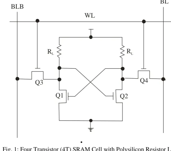
4T SRAM Cell with Polysilicon Resistor Load
The main advantage of static 4T cells with polysilicon resistor load (PRL) (Fig. 3.2) is the approximately 30% smaller area as compared to 6T SRAM cells. Due to the higher electron mobility (µn/µp = 1.5 − 3), all transistors in a PRL cell are normally NMOS. The
load resistors serve to compensate for the off state leakage of the pull down devices. On one hand, the values of RL must be as high as possible to retain a reasonable noise margin
NML, i.e., to limit the “0” level rise and reduce the static power consumption. On the other hand, a high RL severely
increases the low-to-high propagation delay if VDD /2 precharge is used and it also increases the cell size. Furthermore,
precharging the bit lines to VDD /2 can compromise the cell stability with scaling of the VDD /VTH ratio. Precharge of
ISSN(Online): 2319-8753 ISSN (Print): 2347-6710
I
nternational
J
ournal of
I
nnovative
R
esearch in
S
cience,
E
ngineering and
T
echnology
(A High Impact Factor, Monthly, Peer Reviewed Journal) Visit: www.ijirset.com
Vol. 8, Issue 8, August 2019
RL is put by the requirement to provide a pull-up current of at least two orders of magnitude larger than the leakage
current [3]. The lower limit on RL is put by the required noise immunity and power consumption requirements. The
technological variations of RL caused by the limitations of doping and annealing techniques pose another constraint on
the increase of RL.
BLB
WL
BL
R
LR
LQ3
Q1
Q2
Q4
•
• Fig. 1: Four Transistor (4T) SRAM Cell with Polysilicon Resistor Load •
Historically, 4T polysilicon resistor load cells are the remnants of the pre-CMOS tech- nologies. Ratioed inverters comprising the cell have lower gain in the transition region and produce inherently less steep VTCs, which reflects on the SNM values and the recovery time from a metastable state [29] of such cells. The reduction of VDD from the
standard 5V to 3.3V, 2.5V and so on, i.e., the switch from constant-voltage scaling to constant-field scaling to combat the short channel effects, revealed non satisfactory low-voltage stability of the PRL cells. Moreover, the extra technological steps of forming high resistivity polysilicon are not a part of the standard logic technological process. Insufficient tolerance to soft errors.
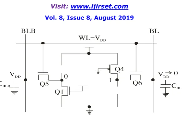
Memory Write Process
Essentially, writing to memory is a two step process. The first step involves the decoding of the memory address and conditioning the bitlines to hold the proper values to be stored into memory. The second step includes turning on the access transistors and allowing the cell to be overwritten with the new data. The speed of a write access is determined by the time it takes to decode the address plus the time to pull the word line high and pass the data from the bitlines to the cell. The write operation is similar to resetting an SR latch. One of the bit lines, e.g., BL in Fig.2, is driven from precharged value (VDD) to the ground potential by a write driver through transistor Q6. If
ISSN(Online): 2319-8753 ISSN (Print): 2347-6710
I
nternational
J
ournal of
I
nnovative
R
esearch in
S
cience,
E
ngineering and
T
echnology
(A High Impact Factor, Monthly, Peer Reviewed Journal) Visit: www.ijirset.com
Vol. 8, Issue 8, August 2019
Q5 Q1
Q6 Q4
1
BLB BL
WL=VDD
VDD
CBLB
0 VDD
CBL
0
Fig. 2: Simplified Model of a 6T CMOS SRAM Cell During a Write Operation
Lower case letters written in these names designates which type of pass transistors the memory latch uses to access the bitlines. Following the previous example, the name that is used from now on for the CMOS Virtual GND/VDD memory
is VGVC. In the last column additional transistors used with the standard 6T SRAM cell are shown.
Table 2: The 6T memory cell and its seven novel variations
Fig.3 Cell Description Abbreviated Name
Additional Transistor a. Standard SRAM with nMOS access Transistor 6T
b. 6T with nMOS access and Virtual GND Transistor VGn TVG c. 6T with nMOS access and Virtual VDD Transistor VVn TVV
d. 6T with nMOS access and Virtual GND/ VDD Transistor VGVn TVG and TVV
e. SRAM with CMOS TG access Transistor 8T TG f. 8T with TG access and Virtual GND Transistor VGc TVG and TG g. 8T with TG access and Virtual VDD Transistor VVc TVV and TG
h. 8T with TG access and Virtual GND/VDD Transistor VGVc TVG, TVV and
TG
6T with Gated GND/VDD (VGVn) Structure
Schematic of VGVn structure shown in Fig 3 has one extra pMOS and one nMOS transistor insertion. Control signals are VSp and VSn respectively.
Here both VSp and VSn signal by controlling pMOS and nMOS provides the gated supply for VDD and GND
respectively. Thus these transistors become virtual supply transistors. As this structure eliminates all the three types of short circuits i.e. One-to-GND, VDD-to-Zero and Short-VDD-GND can be expected most power efficient structure
ISSN(Online): 2319-8753 ISSN (Print): 2347-6710
I
nternational
J
ournal of
I
nnovative
R
esearch in
S
cience,
E
ngineering and
T
echnology
(A High Impact Factor, Monthly, Peer Reviewed Journal) Visit: www.ijirset.com
Vol. 8, Issue 8, August 2019
Fig. 3: Schematic Designing of VGVn
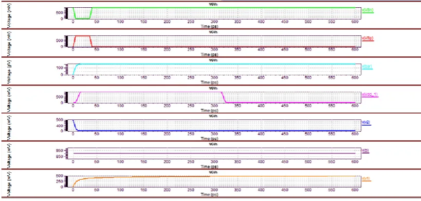
Fig. 4 depicts simulated waveforms for both VSp and VSn control signals with other signals. Power may be optimized by this structure but situation is different in case of delay. VSp and VSn both providing complimentary pulses at the switching of write enabling signal for duration sufficient to provide cut off from supplies at that time. This will effectively reduce short circuit power losses. That will be apparent from power result obtained after simulation.
ISSN(Online): 2319-8753 ISSN (Print): 2347-6710
I
nternational
J
ournal of
I
nnovative
R
esearch in
S
cience,
E
ngineering and
T
echnology
(A High Impact Factor, Monthly, Peer Reviewed Journal) Visit: www.ijirset.com
Vol. 8, Issue 8, August 2019
The details of timing signals in waveforms simulation are as follows:
Vdd_1- Write Enable Signal
b- Bit Line Signal
bar- Inverted Bit Line Signal
v1- Internal Node corresponding to Bit Line
v2- InternalNode corresponding to Inverted Bit Line
VSp- Control Signal for Virtual VDD Transistor
VSn- Control Signal for Virtual GND Transistor
Timing of nodes for pulling up and down is changed as it happens with every changed design.
III. RESULTS AND PERFORMANCE ANALYSIS
Here we will show the results obtained after simulation and then analyze the performance on the basis of these results first for power and delay then for area.
Power and Delay
Simulations of the 6T SRAM and its seven variations were run using the Tanner Tool simulator. This section reports the measured power and delay values gathered from those simulations. The power-delay product is also reported with the results since typically it is a more effective method of comparing data and not as easily manipulated by changing voltage levels or simulation times.
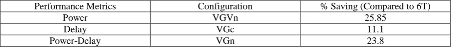
On the basis of this table we can represent best performance results in tabular form as shown below in Table 2:
Table 2: Best Performance Results
Performance Metrics Configuration % Saving (Compared to 6T)
Power VGVn 25.85
Delay VGc 11.1
Power-Delay VGn 23.8
Using the 6T SRAM as a standard for comparison, the VGVn latch demonstrates a 25.85% decrease in power dissipation. Delay is reduced by 11.1% when the VGc cell is used in memory write operations. In terms of the power-delay product, the VGn SRAM exhibited 23.8% savings over the 6T cell. Based on the discussion given in 4, the memory cells performed as would be expected: the virtual source transistors helped to reduce power and including TG in the memory cells decreased the speed to overwrite the stored value. An exception to this is the 8T memory.
IV. CONCLUSION
The most successful designs in terms of power consumption, delay, power-delay product and size are reviewed below.
Lowest Power Consumption: In comparison with the 6T memory cell, VGVn reduces the overall power used during a write cycle by 25.85%. This confirms that virtual source transistors are effective in eliminating short circuits that exist while switching the data stored in memory cells.
Shortest Delay: Through the combined efforts of the virtual ground transistor and the CMOS transmission gates, VGc is able to reduce the delay to store data by 11.1%.
ISSN(Online): 2319-8753 ISSN (Print): 2347-6710
I
nternational
J
ournal of
I
nnovative
R
esearch in
S
cience,
E
ngineering and
T
echnology
(A High Impact Factor, Monthly, Peer Reviewed Journal) Visit: www.ijirset.com
Vol. 8, Issue 8, August 2019
Smallest Size: Although VVn has smallest size after 6T latch but VGn latch is a good option for memory use since only one extra nMOS transistor and with 18.5% more area is needed and it uses less power than the standard 6T memory.
REFERENCES
[1] Anie Jain and Shyam Akashe, “Optimization of Low Power 7T SRAM Cell in 45nm Technology”, Advanced Computing & Communication Technologies (ACCT), Jan. 2012, pp. 324-327.
[2] David Hentrich, Erdal Oruklu and Jafar Saniie, “Performance evaluation of SRAM cells in 22nm predictive CMOS technology”, Electro/Information Technology (EIT), June 2009, pp. 470-475.
[3] Prashant Upadhyay, Mr. Rajesh Mehra, Niveditta Thakur, “Low power design of an SRAM cell for portable devices”, Computer and Communication Technology (ICCCT), Sept. 2010, pp. 255-259. [4] H.P Rajani, Hansraj Guhilot and S.Y Kulkanri, “Novel stable sram for ultra low power deep submicron cache memories”, Recent Advances in Intelligent Computational Systems (RAICS), Sept. 2011, pp. 489-492.
[5] Hiroaki Okuyama, Takeshi Nakano, Shuichi Nishida, Etsuro Aono. Hisahiro Satoh and Shigeru Akita, “A7.5-ns 32Kx8 CMOS SRAM”, IEEE Journal of solid-state circuits, vol. 23, no. 5, Oct. 1988.
[6] Masaya Sumita, Shiro Sakiyama, Masayoshi Kinoshita, Yuta Araki, Yuichiro Ikeda, and Kohei Fukuoka., “Mixed body bias techniques with Fixed Vt and Ids Generation Circuits”, IEEE Journal of solid-state circuits, vol. 40, no. 1, Jan. 2005.
[7] Budhaditya Majumdar and Suman Basu, “Low power single bitline 6T SRAM cell with high read stability”, Recent Trends in Information Systems (ReTIS), Dec.2011, pp. 169-174.
[8] Ramy E. Aly, A. Bayoumi and Mohamed Elgamel, “Dual Sense Amplified Bit Lines (DSABL) Architecture for Low-Power SRAM Design”,
IEEE Journal of solid-state circuits, vol. 54, no. 4, April 2005.
[9] Shin-Pao Cheng and Shi-Yu Huang, “A Low-Power SRAM Design Using Quiet-Bitline Architecture”, Proceedings of the 2005 IEEE International Workshop on Memory Technology, Design, and Testing, 2005.
[10] Hong Zhu and Volkan Kursun, “Application-specific selection of 6T SRAM cells offering superior performance and quality with a triple-threshold-voltage CMOS technology”, Quality Electronic Design (ASQED), July 2011, pp. 68-73.
[11] Zhiyuan Yu, Yinhui Chen, Haiqing Nan, Wei Wang and Ken Choi, “Design of a novel low power 6-T CNFET SRAM cell working in sub-threshold region”, Electro/Information Technology (EIT), May 2011, pp. 1-5.
[12] Hirdaya Narain Mishra and Yashwanta Kumar Patel, “Design, simulation and characterization of memory cell array for low power SRAM using 90nm CMOS technology”, Power, Control and Embedded Systems (ICPCES), Dec. 2010, pp. 1-3.
[13] Kong Zhi Hui and Do Anh Tuan, “A 16Kb 10T-SRAM with 4x read-power reduction”, Circuits and Systems (ISCAS), June 2010, pp. 3485-3488.
[14] S. Panda, N.Mohan Kumar and C.K. Sarkar, “Power, delay and noise optimization of a SRAM cell using a different threshold voltages and high performance output noise reduction circuit”, Computers and Devices for Communication (CODEC), 2009, pp. 1-4.
[15] Yen-Ting Chiang and Yen-Jen Chang, “A New SRAM Cell Design for Both Power and Performance Efficiency”, Memory Technology, Design, and Testing (MTDT), 2009, pp. 13-19.