Implementation Of Two Bit Sequential Multiplier For Low Area
Boya Mahendra
P1
P
, T.Chakrapani
P2
P
K.Prasad Babu
P3
P
H.Devanna
P4
P
K.Sudhakar
P5
P
1 ,
P
Mtech VLSISD 13G31D5703, ECE, JNTUA/SJCET, Yerrakota kurnool, Andhra Pradesh 518360, India, [email protected]
P
2
P
Associate Professor, ECE, JNTUA/SJCET,
Yerrakota kurnool, Andhra Pradesh 518360, India, [email protected]
P
3
P
Assistant Professor ECE, JNTUA/SJCET,
Yerrakota kurnool, Andhra Pradesh 518360, India, [email protected]
P
4
P
Associate Professor ECE, JNTUA/SJCET,
Yerrakota kurnool, Andhra Pradesh 518360, India, [email protected]
P
5
P
Associate Professor & HOD ECE dept, JNTUA/SJCET,
Yerrakota kurnool, Andhra Pradesh 518360, India, [email protected]
Abstract
In this project work, design is based on a 2-bit sequential multiplier, with 8-bit A and B inputs and a 16-bit result. This multiplier has an 8-bit bi-directional I/O for inputting its A and B operands, and outputting its 16-bit output one byte at a time. The multiplexed bi-directorial data-bus is used to reduce the total number of pins of the multiplier. Verilog code is used for entire design of project. Modules such as Register, adder, shifter, multiplexer, tristate bus, controller, datapath and Multiplier are designed.
Keywords:
Sequential Multiplier, Multiplexer, Low Area, Verilog1.
Introduction
The project is the design of a 2-bit sequential multiplier, with 8-bit A and B inputs and a 16-bit result. The block diagram of the circuit to be designed is shown in Figure. This multiplier has an 8-bit bi-directional I/O for
inputting its A and B operands, and outputting its 16-bit output one byte at a time.
Multiplication begins with the start pulse, and the databus will contain operands A and B in two consecutive clock pulses. After accepting these data inputs, the multiplier begins its multiplication process and when it is completed, it starts sending the result out on the databus. When the least significant byte is placed on databus, the Lsb_out output is issued, and for the most-significant byte, msb_out is issued. When both bytes are outputted, done becomes 1, and the multiplier is ready for another set of data.
The multiplexed bi-directorial databus is used to reduce the total number of pins of the multiplier.
Figure: Multiplier Block Diagram
2.
Shift-and-Add Multiplication
When designing multipliers there is always a compromise to be made between how fast the multiplication process is done and how much hardware we are using for its implementation. A simple multiplication method that is slow, but efficient in use of hardware is the shift-and-add method. In this method, depending on bit i of operand A, either operand B is added to the collected partial result and then shifted to the right (when bit i is 1), or (when bit i is 0) the collected partial result is shifted one place to the right without being added to B. This method is justified by considering how binary multiplication is done manually
.
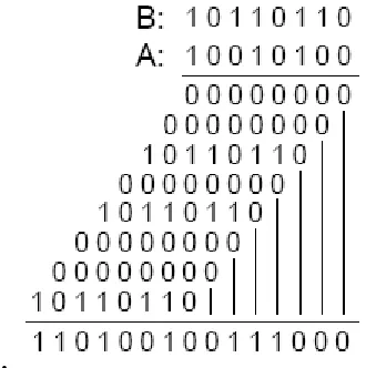
Figure shows manual multiplication of two 8-bit binary numbers.
Figure:
We start considering bits of A from right to left. If a bit value is 0 we select 00000000 to be added with the next partial product, and if it is a 1, the value of B is selected. This process repeats, but each time 00000000 or B is selected, it is written one place to the left with respect to the previous value. When all bits of A are considered, we add all calculated values to come up with the multiplication results.
Understanding hardware implementation of this procedure becomes easier if we make certain modifications to this procedure. First, instead of having to move our observation point from one bit of A to another, we put A in a shift register, always observe its right-most bit, and after every calculation, we move it one place to the right, making its next bit accessible.
Second, for the partial products, instead of writing one and the next one to its left, when writing a partial product, we move it to the right as we are writing it, and the next one will not have to be shifted. Finally, instead of calculating all partial products and at the end adding them up, when a partial product is calculated, we add it to the previous partial result and write the newly calculated value as the new partial result. Therefore, if the bit of A that is being observed is 0, 00000000 is to be added to the previously calculated partial result, and the new value should be shifted one place to the right. In this case, since the value being added to the calculated new sum must be shifted one place to the right. This is called add-and-shift. Repeating the above procedure, when all bits of A are shifted out, the partial result becomes the final multiplication result. We use a 4-bit example to clarify the above procedure.
partial result is 00000000, adding is not necessary, and only shifting the partial result is sufficient. This process is called shift. However, if bit of A being observed is 1, B is to be added to the previously calculated partial result, and
t
he calculated new sum must be shifted one place to the right. This is called add-and-shift. Repeating the above procedure, when all bits of A are shifted out, the partial result becomes the final multiplication result. We use a 4-bit example to clarify the above procedureAt this time, because A[0] is 0, 0000 + P is calculated (instead of B + P). This value is 00110, the right most bit of which is shifted into A, and the rest replace P. This process repeats 4 times, and at the end of the 4th cycle, the multiplication result becomes available in P and A. The least significant 4 bits of the result are in A and the
most-significant bits are in P. The example used here performed 9*13 and 117 was obtained as the result of this operation.
3.
Sequential Multiplier Design
The multiplication process discussed in the previous section justifies the hardware implementation that is being discussed here.
3.1
Control Data Partitioning
The multiplier has a datapath and a controller. The data part consists of registers, logic units and their interconnecting busses. The controller is a state machine that issues control signals for control of what gets clocked into the data registers.
As shown in Figure, the data path registers and the controller are triggered with the same clock signal. On the rising edge of a clock the controller goes into a new state. In this state, several control signals are issued, and as a result the components of the datapath start reacting to these signals.
The time given for all activities of the datapath to stabilize is from one edge of the clock to another. Values that are propagated to the inputs of the datapath registers are clocked into these register with every clock edge.
3.2 Multiplier Datapath
Figure shows the datapath of the sequential multiplier. As shown, P and B are 8-bit registers and A is an 8-bit shift-register. An adder, a multiplexer and a tri-state buffer constitute the other components of this datapath.
Control signals that are outputs of the controller and inputs of the datapath are shown in bold in Figure 11.5 next to the data component that they control. These control signals control register clocking, bus assignments and logic unit output selections. The input databus connects to the inputs of A and B to load multiplier and multiplicand into these registers. This bi-directional bus is driven by the
output of P through an octal state buffer, and by the tri-state output of A. This bi-directional bus is driven by the output of P through an actual state buffer, and by the tri-state output of A. These tri-tri-states become active when multiplication result is ready.
Figure: Multiplier circuit
The output from B and P are put into an 8-bit adder for partial result in P to be added to B. The output of this adder (P+B) feeds one side of a multiplexer. The other side of the multiplexer is driven by the P output, (P+0). The sel_sum control input determines if P+B or P+0 is to go on the multiplexer output.The AND gate shown in selects carry-out from the adder or 0 depending of the value of sel_sum control input. This value is concatenated to the left of the multiplexer output to form a 9-bit vector. This vector has P+B or P+0 with a carry to its left. The right-most bit of this 9-bit vector is split and goes into the serial input of the shift-register that contains A, and the other eight bits go into register P. Note that concatenation of the AND gate output to the left of multiplexer output and splitting the right bit from this 9-bit vector, effectively produces a shifted result that is clocked into P. When the output enable (oe) of the shift-register is active, im_data is placed on the data bi-directional port of the shift-register. Otherwise, data is float. Placement of im_data on data is also conditioned by ~s1, so that data is driven only when not used as input. Another component of the datapath of Figure is the multiplexer of Figure . This multiplexer selects its a or b input depending on the value of sel. In addition, the multiplexer has a zero input that when 1, it forces its output to 8’h0. Since the multiplexer output connects to P, its zeroing feature is used for initial resetting of the P register. As shown in Figure, an octal tri-state buffer connects the output of P to the bi-directional databus. The Verilog Code of this buffer is shown in Figure . The en input of this structure becomes active, when the most significant byte of the result that is in P is to go on the multiplier output (databus).
Figure: adder circuit
Figure: shifter circuit
Figure: Register circuit
Figure: multiplexer circuit
Figure: Tristate Buffer circuit
Figure: datapath circuit
Figure: controller circuit
The multiplier controller is a finite state machine that has two starting states, eight multiplication states, and two ending states. States and their binary assignments are shown in Figure . In the `idle state the multiplier waits
for `start while loading A. In `init, it loads the second
operand B. In `m1 to `m8, the multiplier performs add-and-shift of P+P, or P+0, depending on A0. In the last two states (`rslt1 and 1rslt2), the two halves of the result are put
on databus.
Figure: multiplier circuit
This block declares datapath ports, and uses a single always block to issue control signals and make state transitions. At the beginning of this always block all control signal outputs are set to their inactive values. This eliminates unwanted latches that may be generated by the synthesis tool for these outputs. The 4-bit current variable represents the currently active state of the machine. When current is `idle and start is 0, the done output remains high. In this state if start becomes 1, control signals load_A, clr_P and load_P become active to load A with databus and clear the P register. Clearing P requires clr_P to put 0’s on the multiplexer output by disabling it and loading the 0’s into P by asserting load_P. In `m1 to `m8 states, A is shifted, P is
loaded, and if A0 is 1, sel_sum is asserted. As discussed in relation to datapath, sel_sum controls shifted P+B or shifted P+0) to go into P. In the result states lsb_out and msb_out are asserted in two consecutive clocks in order to put A and P on the databus, respectively.
4.
CONCLUSION &
FUTURESCOPE
Power dissipation in multiplier designs has been much-researched in recent years, due to the importance of the multiplier circuit in a wide variety of microelectronic systems. The focus of multiplier design has traditionally been delay optimization, although this design goal has recently been supplemented by power consumption considerations. Our goal has been first to understand how power is dissipated in multipliers, and secondly to devise ways to reduce this power consumption. Power savings of up to 25% were achieved, along with reductions in die area and interconnect. We have presented an investigation of multiplier power dissipation, along with some techniques which allow reductions in power consumption for this circuit. Given the importance of multipliers, it is likely that further research efforts will be directed at optimizing this block for delay and power efficiency.
REFERENCES
[1] A. Abnous and J. Rabaey, “Ultra-low-power domain-specific multimedia processors,” in VLSI Signal Processing, IX, pp.461-470, Oct. 1996.
[2] I. Abu-Khater, A. Bellaouar, and M. Elmasry, “Circuit techniques for CMOS low-power high-performance multipliers”, IEEE J. Solid-State Circuits, vol.31, no.10, pp.1535-1546, Oct. 1996.
[3] H. A. Al-Twaijry, Area and Performance Optimized CMOS Multipliers. Ph.D. dissertation, Stanford University, Aug. 1997.
[4] M. Alidina, et. al., “Precomputation-based sequential logic optimization for low power,” IEEE Trans. VLSI Systems, vol.2, no.4, pp.426-436, Dec. 1994.
[5] F.S. Anderson, et. al., “The IBM system 360/91 floating point execution unit,” IBM J. Res. Develop., vol.11, pp.34-53, Jan. 1967.
[6] E. de Angel and E.E. Swartzlander, Jr., “Survey of low power techniques for VLSI design,” in Proc. 8th Annual IEEE Int. Conf. Innovative Systems in Silicon, pp.159-169, Oct. 1996.
[7] E. de Angel and E.E. Swartzlander, Jr., “Low power parallel multipliers,”in VLSI Signal Processing, IX, pp.199-208, Oct. 1996.
[8] E. de Angel, Low Power Digital Multiplication. Ph.D. dissertation, The University of Texas at Austin, 1996. [9] E. de Angel and E.E. Swartzlander, Jr., “Switching activity in parallel multipliers,” in Proc. 35th Asilomar Conf. Signals, Systems and Computers, pp.857-860, Nov. 2001.
[10] TSMC 0.18μm Process 1.8-Volt SAGE-X Standard Cell Library Databook. Artisan Components, Inc., Oct. 2001.
[11] A. Bellaouar and M. Elmasry, Low-power Digital VLSI Design: Circuits and Systems. Kluwer Academic Publishers, 1995.
[12] G.W. Bewick, Fast Multiplication: Algorithms and Implementation. Ph.D. dissertation, Stanford University, Feb. 1994.