Induction Motor Drive Fed With An Integrated
Dynamic Voltage Restorer For Power Quality
Improvement
SINGAMPALLI.REVATHIM-tech Student Scholar
Department of Electrical & Electronics Engineering, Baba Institute of Technology & Sciences,
Visakhapatnam (Dt); A.P, India. Email:[email protected]
TERUKOTI DIVYA Assistant Professor
Department of Electrical & Electronics Engineering, Baba Institute of Technology & Sciences,
Visakhapatnam (Dt); A.P, India. Email:[email protected]
Abstract- This paper proposes an integrated DVR is used for power quality improvement fed with Induction Motor Drive. The voltage disturbances predominately contain the voltage sags, swells (power, speed, torque and possible stall) harmonics (losses and torque), unbalanced quite short interruptions, transient over voltage and under voltage and flicker. The preliminary operation of the DVR is to inject a voltage of the associated magnitude, phase positioning and additional frequency in progression with the distribution feeder to monitor and stay in the desired amplitude and waveform for load voltage even though the voltage is out of balance or distorted. Introduction motors are widely used in industrial applications for their intrinsic ruggedness and reduced cost. In the project DVR inject an appropriate voltage magnitude with an appropriate phase angle dynamically. This project is extended with integrated DVR is fed with Induction motor drive. The Induction motor stator current speed and torque responses are studied.
Keywords: Dynamic Voltage Restorer, Induction motor drive, Power Quality Problems.
I. INTRODUCTION
Widespread use of electronics in everything from home electronics to the control of massive and costly industrial processes has raised the awareness of power quality. Power quality or more specifically a power quality disturbance is generally defined as any change in power (voltage, current or frequency) that interferes with the normal operation of electrical equipment. The study of power quality and ways to control it is a concern for electric utilities, large industrial companies, businesses and even home users. The study has intensified as equipment has become increasingly sensitive to even minute changes in the power supply voltage, current, and frequency[1].
Power Quality problems encompass a wide range of disturbances such as voltage sags/swells, flicker, harmonics distortion, impulse transient, and interruptions. These voltage interruptions inauspiciously effect voltage vulnerable load appliances in automatic production lines, high precision processing, buildings, rolling mills, textile mills. These kinds of voltage and challenging experience interferences resulting in substantial cost-effective and or data losses [2]. Voltage sags are referred to as reducing of root mean square voltage at power frequency for durations from 0,5 cycles to 1 minute.
It is actually therefore possible for the sag of a short-time moment to cause problems in some sensitive equipment [3-5]. Voltage sags may be caused by switching actions associated with impermanent disconnection of supply, the progression inrush current associated with the commencing of induction motor loads or steady stream of fault currents due to short circuit faults which includes single line to ground fault in a power system (SLG). These kinds of phenomena would probably originate from the customers system or from a public supply network [6]. Voltage swells are brief magnifications in root mean square voltage between 1,1 pu and 1,8 pu at the power frequency amounts of time from 0,5 cycles in 1 minute.
A DVR is often familiar to alleviating the impact of unusually high voltage variations while making use of a highly effective custom electric power equipment that is to say dynamic voltage restorer. It contains an electric power storage device, filtration systems, voltage source inverters and also injection transformer. There are numerous categories of regulating approaches being employed for mitigation of abnormal voltages. Voltage Restorer (DVR) is a modified power apparatus that is utilized to enhance voltage stability i.e. to minimize the power quality problems in electrical power system network. The important parts of the DVR comprise of voltage source inverter (VSI), booster transformers, filter and a dc energy source. The principle of the DVR is utilized to inject the voltage in series and in synchronism with the standard voltages with a goal to compensate voltage influences [7].
Among the power quality problems (sags, swells, harmonics…) voltage sags are the most severe disturbances[8-10]. In order to overcome these problems the concept of custom power devices is introduced recently. One of those devices is the Dynamic Voltage Restorer (DVR), which is the most efficient and effective modern custom power device used in power distribution networks. DVR is a recently proposed series connected solid state device that injects voltage into the system in order to regulate the load side voltage. It is normally installed in a distribution system between the supply and the critical load feeder at the point of common coupling (PCC). Other than voltage sags and swells compensation, DVR can also added other features like: line voltage harmonics compensation, reduction of transients in voltage and fault current limitations[11].
causes for malfunctioning in production plants[12]. Voltage sag is short term shrinkage in voltage magnitude. According to IEEE standard 1159 voltage sag is “a decrease in RMS voltage between 10 to 90 % at a power frequency for durations from 0.5 cycles to 1 minute” [13].
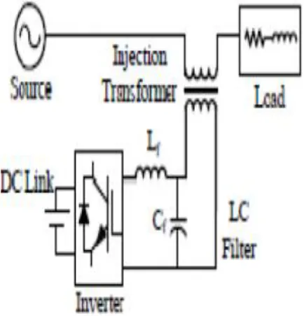
Fig.1. Basic Components of a DVR.
During voltage sag, the DVR injects a voltage to restore the load supply voltages. The DVR needs a source for this energy. Two types of system are considered; one using stored energy to supply the delivered power as shown in Figure1, and the other having no internal energy storage. There are a number of voltage swell/sag mitigating schemes available but the use of custom power service is deliberated to the most productive scheme. This paper introduce basic concept of DVR (Dynamic Voltage Restore). DVR inject a compatible voltage magnitude with
a compatible phase angle dynamically. Dynamic
compensating signals are determine based on the difference between desired and actual values. Main components of DVR are voltage source converter, injecting transformer, passive filter, and energy storage device. The performance of DVR depends on the efficiency control technique of switching of voltage source inverter (VSI). In this paper Hysteresis Voltage control based simple control method is used to compensate voltage sag/swell.
This paper introduces Dynamic Voltage Restorer and its operating principle. Then, an integrated DVR based Induction motor is used to compensate voltage swells/sags. At the end, MATLAB/SIMULINK model based simulated results were extant to certify the productiveness of the suggested control method of DVR.
II. THREE-PHASE SERIES INVERTER
A. Power Stage
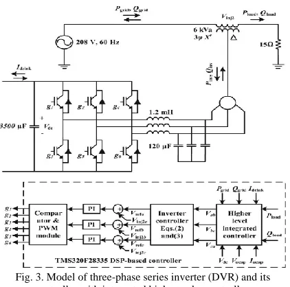
The one-line diagram of the system is shown in Fig. 2. The power stage is a three-phase voltage source inverter, which is connected in series to the grid and is responsible for compensating the voltage sags and swells; the model of the series DVR and its controller
is shown in Fig. 3. The inverter system consists of an insulated gate bipolar transistor (IGBT) module, its gate-driver, LC filter, and an isolation transformer. The dc-link voltage Vdc is regulated at 260 V for optimum performance of the converter and the line– line voltage Vab is 208 V; based on these, the modulation index m of the inverter is given by
(1) Where n is the turn’s ratio of the isolation transformer.
Substituting n as 2.5 in (1), the required modulation index is calculated as 0.52. Therefore, the output of the dc–dc converter should be regulated at 260 V for providing accurate voltage compensation. The objective of the integrated UCAPDVR system with active power capability is to compensate for temporary voltage sag (0.1–0.9 p.u.) and voltage swell (1.1–1.2 p.u.), which last from 3 s to 1 min.
B. Controller Implementation
There are various methods to control the series inverter to provide dynamic voltage restoration and most of them rely on injecting a voltage in quadrature with advanced phase, so that reactive power is utilized in voltage restoration. Phaseadvanced voltage
restoration techniques are complex in
implementation, but the primary reason for using these techniques is
Fig. 3. Model of three-phase series inverter (DVR) and its controller with integrated higher order controller.
to minimize the active power support and thereby the amount of energy storage requirement at the dc-link in order to minimize the cost of energy storage. However, the cost of energy storage has been declining and with the availability of active power support at the dc-link, complicated phase-advanced techniques canbe avoided and voltages can be injected in-phase with the system voltage during a voltage sag or a swell event. The controlmethod requires the use of a PLL to find the rotating angle. As discussed previously, the goal of this project is to use the active power capability of the UCAP-DVR system and compensate temporary voltage sags and swells. The inverter controller implementation is based on injecting voltages in-phase with the supply-side line–neutral voltages. This requires PLL for estimating θ, which has been implemented using the fictitious power method described. Based on the estimated θ and the line–line source voltages, Vab, Vbc, and Vca (which are available for this delta-sourced system) are transformed into the d–q domain and the line– neutral components of the source voltage Vsa, Vsb, and Vsc, which are not available, can then be estimated using
(2)
(3)
(4)
These voltages are normalized to unit sine waves using line–neutral system voltage of 120 Vrms as reference and compared to unit sine waves in-phase with actual system voltages Vs from (3) to find the injected voltage references Vref necessary to maintain a constant voltage at the load terminals, where m is 0.52 from (1). Therefore, whenever there is a voltage sag or swell on the source side, a corresponding voltage Vinj2 is injected in-phase by the DVR and UCAP system to negate the effect and retain a constant voltage VL at the load end. The actual active and reactive power supplied by the series inverter can be computed using (4) from the rms values of the injected voltage Vinj2a and load current ILa, and ϕ is the phase difference between the two waveforms.
III. UCAP AND BIDIRECTIONAL DC–DC CONVERTER
A. UCAP Bank
The choice of the number of UCAPs necessary for providing grid support depends on the amount of support needed, terminal voltage of the UCAP, dc-link voltage, and distribution grid voltages. In this paper, the experimental setup consists of three 48 V, 165F UCAPs (BMOD0165P048) manufactured by Maxwell Technologies, which are connected in series. Therefore, the terminal voltage of the UCAP bank is 144 V and the dc-link voltage is programmed to 260 V. This would give the dc–dc converter a practical operating duty ratio of 0.44–0.72 in the boost mode while the UCAP is discharging and 0.27– 0.55 in the buck mode while the UCAP is charging from the grid through the dc-link and the dc–dc converter. It is practical and cost-effective to use three modules in the UCAP bank. Assuming that the UCAP bank can be discharged to 50% of its initial voltage (Vuc,ini) to final voltage (Vuc,fin) from 144 to 72 V, which translates to depth of discharge of 75%, the energy in the UCAP bank available for discharge is given by
(5)
B. Bidirectional DC–DC Converter and Controller
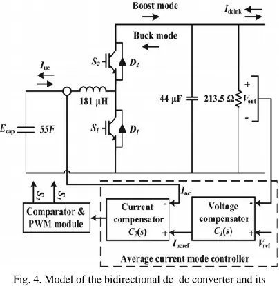
controller are shown in Fig.4, where the input consists of three UCAPs connected in series and the output consists of a nominal load of 213.5 Ω to prevent operation at no-load, and the output is connected to the dc-link of the inverter. The amount of active power support required by the grid during a voltage sag event is dependent on the depth and duration of the voltage sag, and the dc–dc converter should be able to withstand this power during the discharge mode. The dc–dc converter should also be able
Fig. 4. Model of the bidirectional dc–dc converter and its controller.
to operate in bidirectional mode to be able to charge or absorb additional power from the grid during voltage swell event. In this paper, the bidirectional dc–dc converter acts as a boost converter while discharging power from the UCAP and acts as a buck converter while charging the UCAP from the grid. A bidirectional dc–dc converter is required as an interface between the UCAP and the dc-link since the UCAP voltage varies with the amount of energy discharged while the dc-link voltage has to be stiff. Therefore, the bidirectional dc–dc converter is designed to operate in boost mode when the UCAP bank voltage is between 72 and 144 V and the output voltage is regulated at 260 V. When the UCAP bank voltage is below 72 V, the bidirectional dc–dc converter is operated in buck mode and draws energy from the grid to charge the UCAPs and the output voltage is again regulated at 260 V.
Average current mode control, which is widely explored in literature, is used to regulate the output voltage of the bidirectional dc–dc converter in both buck and boost modes while charging and discharging the UCAP bank. This method tends to be more stable when compared to other methods such as voltage mode control and peak current mode control.
Average current mode controller is shown in Fig. 4, where the dc-link and actual output voltage Vout is compared with the reference voltage Vref and the error is passed through the voltage compensator C1(s), which generates the average reference current Iucref. When the inverter is discharging power into the grid during voltage sag event, the dc-link voltage Vout tends to go below the reference Vref and the error is positive; Iucref is positive and the dc–dc converter operates in boost mode. When the inverter is absorbing power from the grid during voltage swell event or charging the UCAP, Vout tends to increase above the reference Vref and the error is negative; Iucref is negative and the dc–dc converter operates in buck mode. Therefore, the sign of the error between Vout and Vref determines the sign of Iucrefand thereby the direction of operation of the bidirectional dc–dcconverter. The reference current Iucref is then compared to the actual UCAP current (which is also the inductor current) Iuc and the error is then passed through the current compensator C2(s). The compensator transfer functions, which provide a stable response, are given by
(6)
(7)
C. INDUCTION MOTOR DRIVE
The induction motor has advantage as simple construction, reliability, raggedness and low cost has found very wide industrial appellations. Furthermore, in contrast to the commutation Dc motor, it can be used in aggressive or volatile environments since there are no problems with spark and corrosion. These advantages, however, are occupied by control problems when using induction motor in speed regulated industrial drives. These advantages, however, are occupied by control problems when using induction motor in speed regulated industrial drives. Speed control (v/f control) of induction motor requires two stage conversion (ac-dc and dc-ac), but most of the classical inverters gives poor performance. Here a Reversing Voltage topology in five level and seven level inverter is implemented for induction motor load which has superior characteristics over traditional topologies in terms of required components as switches, voltage balancing, control requirements and reliability. Here SPWM controller has less complexity.
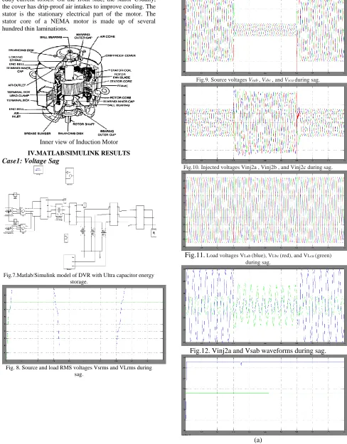
eddy-current losses. On the front side, the stator Usually, the cover has drip-proof air intakes to improve cooling. The stator is the stationary electrical part of the motor. The stator core of a NEMA motor is made up of several hundred thin laminations.
Inner view of Induction Motor
IV.MATLAB/SIMULINK RESULTS Case1: Voltage Sag
Fig.7.Matlab/Simulink model of DVR with Ultra capacitor energy storage.
Fig. 8. Source and load RMS voltages Vsrms and VLrms during sag.
Fig.9. Source voltages Vsab , Vsbc , and Vsca during sag.
Fig.10. Injected voltages Vinj2a , Vinj2b , and Vinj2c during sag.
Fig.11. Load voltages VLab (blue), VLbc (red), and VLca (green) during sag.
Fig.12. Vinj2a and Vsab waveforms during sag.
(b)
(c)
Fig. 13. (a) Currents and voltages of dc–dc converter. (b) Active power of grid, load, and inverter during voltage sag. Case2: Voltage Swell
Fig. 14. Source and load rms voltages Vsrms and VLrms during swell.
Fig.15.Source voltages Vsab, Vsbc, and Vsca during swell.
Fig.16. Load voltages VLab, VLbc, and VLca during swell.
Fig.17.Injected voltages Vinj2a, Vinj2b, Vinj2c during swell.
Fig.18. Vinj2a and Vsab waveforms during swell.
(b)
(c)
Fig. 19. (a) Currents and voltages of dc–dc converter during swell. (b) Active and reactive power of grid, load, and inverter during a
voltage swell.
Fig 20. Matlab/Simulink circuit for DVR with Induction motor drive
Fig 21. Simulation results for stator current,Torque and speed
V. CONCLUSION
In this paper voltage sag compensation using Dynamic Voltage Restorer is considered. Now a days the issues of power quality are very important for customer and utility also. So for this custom power device, Dynamic Voltage Restorer (DVR) is used to mitigate these
power quality problems. Simulation was carried out
with Induction motor drive based DVR with
MATLAB/SIMULINK software. Induction motor
performance is observed for stator current, torque and speed.
REFERENCES
[1] T. Manokaran, V. Rajasekaran, “Power Quality Enhancement In Induction Motor Drives By Using Custom Power Device,”ISSN 1330-3651 (Print), ISSN 1848-6339 (Online) DOI: 10.17559/TV-20130910231852.
[2] T. SRIPAL REDDY, L. RAMESH, JYOTHI RASALA, “Voltage Quality Improvement of Induction Motor Drive using Hysteresis Controlled DVR,” IJSETR ISSN 2319-8885 Vol.04,Issue.33, August-2015, Pages:6595-6599.
[3].Deepak Somayajula, Member, IEEE, and Mariesa L. Crow, Fellow, IEEE” An Integrated Dynamic Voltage Restorer-Ultra capacitor Design for Improving Power Quality of the Distribution Grid” IEEE Transactions On Sustainable Energy, Vol. 6, No. 2, April 2015.
[4] N. H. Woodley, L. Morgan, and A. Sundaram, “Experience with an inverter-based dynamic voltage restorer,” IEEE Trans. Power Del.,vol. 14, no. 3, pp. 1181–1186, Jul. 1999.
[5] S. S. Choi, B. H. Li, and D. M. Vilathgamuwa, “Dynamic voltage restoration with minimum energy injection,” IEEE Trans. Power Syst., vol. 15,no. 1, pp. 51–57, Feb. 2000.
[6] D. M. Vilathgamuwa, A. A. D. R. Perera, and S. S. Choi, “Voltage sag compensation with energy optimized dynamic voltage restorer,” IEEE Trans. Power Del., vol. 18, no. 3, pp. 928– 936, Jul. 2003.
implementation,” IEEE Trans. Ind. Electron., vol. 54, no. 4, pp. 2249–2261,Aug. 2007.
[8] A. Ghosh and G. Ledwich, “Compensation of distribution system voltageusing DVR,” IEEE Trans. Power Del., vol. 17, no. 4, pp. 1030–1036, Oct.2002.
[9] A. Elnady and M. M. A. Salama, “Mitigation of voltage disturbancesusing adaptive perceptron-based control algorithm,” IEEE Trans. PowerDel., vol. 20, no. 1, pp. 309–318, Jan. 2005. [10] P. R. Sanchez, E. Acha, J. E. O. Calderon, V. Feliu, and A. G. Cerrada, “Aversatile control scheme for a dynamic voltage restorer for power quality improvement,” IEEE Trans. Power Del., vol. 24, no. 1, pp. 277–284, Jan.2009.
[11] K. Sahay and B. Dwivedi, “Super capacitor energy storage system for power quality improvement: An overview,” J. Elect. Syst., vol. 10, no. 10,pp. 1–8, 2009.
[12] P. F. Ribeiro, B. K. Johnson, M. L. Crow, A. Arsoy, and Y. Liu, “Energy storage systems for advanced power applications,” Proc. IEEE, vol. 89,no. 12, pp. 1744–1756, Dec. 2001.