A Novel Architecture for Matching of Data
Encoded with an Error-Correcting-Codes
Technique
G.L.Prasanna1, Ch.Vijaya Sree2
PG Student [VLSI], Dept. of ECE, Swamy Vivekanda Engineering College, Bobbili, Andhra Pradesh, India1
Assistant Professor, Dept .of ECE, Swamy Vivekananda Engineering College, Bobbili, Andhra Pradesh, India2
ABSTRACT: To reduce latency and complexity a new architecture for matching the data protected with an error-correcting code (ECC). ECC is usually represented in a systematic form consisting of the raw data and the parity information generated by encoding, the proposed architecture parallelizes the comparison of the data and that of the parity information. A new butterfly-formed weight accumulator (BWA) is proposed for the efficient computation of the Hamming distance for reduce delay and complexity. BWA, the proposed architecture examines whether the incoming data matches the stored data if a certain number of erroneous bits are corrected. For a (40, 33) code, the proposed architecture reduces the latency and the hardware complexity by 32% and 9%, respectively, compared with the most recent implementation.
KEYWORDS: Data comparison, error-correcting codes (ECCs), Ham-ming distance, systematic codes, tag matching.
I. INTRODUCTION
Data comparison circuit is a logic that has many applications in a computing system. For example, to check whether a piece of information is in a cache, the address of the information in the memory is compared to all cache tags in the same set that might contain that address. Another place that uses a data comparison circuit is in the translation look-aside buffer (TLB) unit. TLB is used to speed up virtual to physical address translation.Error correcting codes (ECCs) are widely used in modern microprocessors to enhance the reliability and data integrity of their memory structures. Several error detecting codes (EDCs) and error correcting codes (ECCs) have been proposed so far to improve cache reliability. They range from the simple parity check code to the more complex Single Error Correcting/Double Error Detecting (SEC/DED) ECC (used to protect the L2 and L3 caches in the Itanium microprocessor.
It is widely used in computing systems to performmany operations such as the tag matching in a cache memory and thevirtual-to-physical address translation in a translation lookaside buffer(TLB). Because of such prevalence, it is important to implement thecomparison circuit with low hardware complexity. Besides, the datacomparison usually resides in the critical path of the components that are devised to increase the system performance, e.g., caches and TLBs, whose outputs determine the flow of the succeeding operations in a pipeline. The circuit, therefore, must be designed to have as low latency as possible, or the components will be disqualified from serving as accelerators and the overall performance of the whole system would be severely deteriorated. Thus, it becomes much harder to meet the above design constraints. Despite the need for sophisticated designs as described, the works that cope with the problem are not widely known in the literature since it has been usually treated within industries for their products. Recently, however, triggered the attraction of more and more attentions from the academic field.
II. EXISTING METHOD
n-bit retrieved codeword should first be decoded to extract the original k-bit tag. The extracted k-bit tag is then compared with the k-bit tag field of an incoming address to determine whether the tags are matched or not. As the retrieved codeword should go through the decoder before being compared with the incoming tag, the critical path is too long to be employed in a practical cache system designed for high-speed access.
ii. Direct Compare Method
Direct compare method is one of the most recent solutions for the matching problem. The direct compare method encodes the incoming data and then compares it with the retrieved data that has been encoded as well.Therefore, the method eliminates the complex decoding from the critical path.
iii. Sa-Based Approach
SA-based approach is the one where a special counter is constructed with an additional` building block called saturating adder (SA).The SA-based direct compare architecture reduces the latency and hardware complexity by resolving the aforementioned drawbacks.
B. ADVANCED DATA COMPARISION METHODS a. DMC Encoding
Because of high-speed caches and main memories, which are prone to soft errors, error correcting codes are used in the design and, more recently, in the design of onchip memories.For the encoding Decimal matrix code (DMC) is proposed to assure reliability in the presence of MCUs with reduced performance overheads, and a 4-bit word is encoded based on the proposed technique.
First, during the encoding process, information bits i are fed to the DMC encoder, and then the horizontal redundant bits H and vertical redundant bits V are obtained from the DMC encoder. When the encoding .redundant bits V are obtained by xor operation among the bits per column.
It should be noted that both divide-symbol and arrange-matrix are implemented in logical instead of in physical. Therefore, the proposed DMC does not require changing the physical structure of the memory.
B. XOR BANK
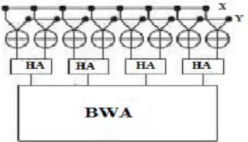
Xor bank represents the array of bit-wise comparators (exclusive OR gates). It performs XOR operations for every pair of bits in X and Y so as to generate a vector representing the bitwise difference of the two codewords. The output from the XOR bank is then fed into BWA consisting of half adders (HAs). The numbers of 1’s are accumulated by passing the value through the BWA.
FIGURE 1: XOR bank structure for (8,4) code
III. PROPOSED ARCHITECTURE
A. BUTTERFLY FORMED WEIGHT ACCUMULATOR
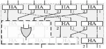
The proposed architecture grounded on the data path design is given below. It contains multiple butterfly-formed weight accumulators (BWAs) proposed to improve the latency and complexity of the Hamming distance computation. The basic function of the BWA is to count the number of 1’s among its input bits.
The proposed architecture consists of multiple stages of HAs as shown in figure where each output bit of a HA is associated with a weight. The HAs in a stage are connected in a butterfly form so as to accumulate the carry bits and the sum bits of the upper stage separately. In other words, both inputs of a HA in a stage, except the first stage, are either carry bits or sum bits computed in the upper stage. This connection method leads to a property that if an output bit of a HA is set, the number of 1’s among the bits in the paths reaching the HA is equal to the weight of the output bit.
B. GENERAL STRUCTURE OF BWA
In above figure 2 for example, if the carry bit of the gray-colored HA is set, the number of 1’s among the associated input bits, i.e., A, B, C, and D, is 2. At the last stage of above figure the number of 1’s among the input bits, d, can be
calculated as .
FIGURE 2 Proposed data path design
The output of the OR-gate tree is connected to the subsequent OR-gate tree at the second level, and the remaining weight bits are connected to the second level BWAs according to their weights.More precisely, the bits of weight w are connected to the BWA responsible for w-weight inputs. Each BWA at the second level is associated with a weight of a power of two that is less than or equal to Pmax, where Pmax is the largest power. As the weight bits associated with the fourth range are all ORed in the revised BWAs, there is no need to deal with the powers of two that are larger than Pmax.
C. GENERAL EXPRESSION FOR THE COMPLEXITY AND THE LATENCY
The complexity as well as the latency of combinational circuits heavily depends on the algorithm employed. In addition, as the complexity and the latency are usually conflicting with each other, it is unfortunately hard to derive an analytical and fully deterministic equation that shows the relationship between the number of gates and the latency for the proposed architecture and also for the conventional SA-based architecture.
To circumvent the difficulty in analytical derivation, we present instead an expression that can be used to estimate the complexity and the latency by employing some variables for the nondeterministic parts. The complexity of the proposed architecture,C, can be expressed as
whereCXOR, CENC, C2nd, CDU, and CBWA(n) are the complexities of XORbanks, an encoder, the second level circuits, the
decision unit, and a BWA forninputs, respectively. Using the recurrence relation,
The latency of the proposed architecture,L, can be expressed as
where LXOR, LENC, L2nd, LDU ,and LBWA(n)are the latencies of an XORbank, an encoder, the second level circuits, the
decision unit, and a BWA forninputs, respectively. Note that the latencies of the OR-gate tree and BWAs for x ≤n
inputs at the second level are all bounded by [log2 n].As one of BWAs at the first level finishes earlier than the other,
some components at the second level may start earlier. Similarly, some BWAs or theOR-gate tree at the second level may provide their output earlier to the decision unit so that the unit can begin its operation without waiting for all of its inputs. In such cases, L2nd and LDU can be partially hidden by the critical path of the preceding circuits, and becomes
shorter than the given expression.
D. DECISION UNIT
The decision unit is infact a combinational logic of which functionality is specified by a truth table that takes the outputs of the preceding circuits as inputs.For the (8, 4) code that the corresponding first and second level circuits are given above, the truth table for the decision unit is described in Table I. Since U and V cannot be set simultaneously.
IV. RESULTS
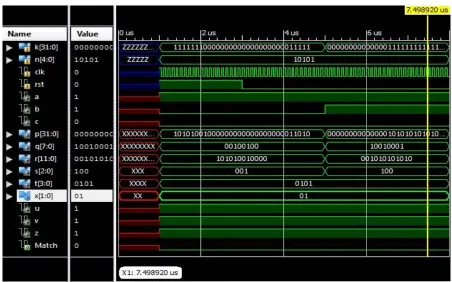
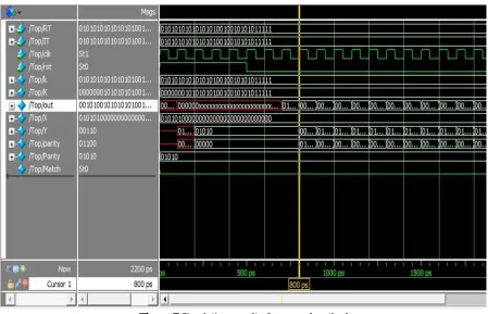
Figure 5 Simulation result of Data match
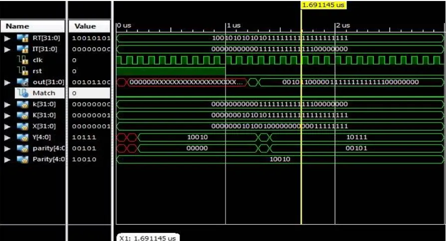
Figure 7 Simulation result of proposed method
V.CONCLUSION
To reduce the latency and hardware complexity, a new architecture has been presented for matching the data protected with an ECC. The proposed architecture examines whether the incoming data matches the stored data if a certain number of erroneous bits are corrected. To reduce the latency, the comparison of the data is parallelized with the encoding process that generates the parity information. The parallel operations are enabled based on the fact that the systematic codeword has separate fields for the data and parity. In addition, an efficient processing architecture has been presented to further minimize the latency and complexity. As the proposed architecture is effective in reducing the latency as well as the complexity considerably, it can be regarded as a promising solution for the comparison of ECC-protected data. Though this brief focuses only on the tag match of a cache memory, the proposed method is applicable to diverse applications that need such comparison.
REFERENCES
[1] J. Chang, M. Huang, J. Shoemaker, J. Benoit, S.-L. Chen, W. Chen, S. Chiu, R. Ganesan, G. Leong, V. Lukka, S. Rusu, and D. Srivastava,“The 65-nm 16-MB shared on-die L3 cache for the dual-core Intel xeon processor 7100 series,” IEEE J. Solid-State Circuits, vol. 42, no. 4, pp. 846–852,
Apr. 2007.
[2] J. D. Warnock, Y.-H. Chan, S. M. Carey, H. Wen, P. J. Meaney, G. Gerwig, H. H. Smith, Y. H. Chan, J. Davis, P. Bunce, A. Pelella, D. Rodko, P.Patel,T.Strach,D.Malone,F.Malgioglio,J.Neves,D.L.Rude, and W.V. Huott “Circuit and physical design implementation of the microprocessor chip for the z Enterprise system,”IEEE J. Solid-State Circuits, vol. 47, no. 1, pp. 151–163,
Jan. 2012.
[3] H. Ando, Y. Yoshida, A. Inoue, I. Sugiyama, T. Asakawa, K. Morita, T. Muta, and T. Motokurumada, S. Okada, H. Yamashita, and Y. Satsukawa, “A 1.3 GHz fifth generation SPARC64 microprocessor, inIEEE ISSCC. Dig. Tech. Papers, Feb. 2003, pp. 246–247.
[4] M. Tremblay and S. Chaudhry, “A third-generation 65nm 16-core 32-thread plus 32-scout-thread CMT SPARC processor,” inISSCC. Dig.Tech. Papers, Feb. 2008, pp. 82–83.
[5] W. Wu, D. Somasekhar, and S.-L. Lu, “Direct compare of information coded with error-correcting codes,” IEEE Trans. Very Large Scale Integr. (VLSI) Syst., vol. 20, no. 11, pp. 2147–2151, Nov. 2012.