Screen printed In
2O
3-SnO
2nanocomposite: Structural and
morphological properties and application for NO
2detection
I. Madhi,a, M. Saadoun and B. Bessaïs
Laboratoire de Photovoltaïque, Centre de Recherche et des Technologies de l’Energie, Technopole de Borj-Cédria, BP 95, 2050 Hammam Lif, Tunisie.
Abstract. In this work, we report on the sensing properties of screen-printed In2O3
(Indium Oxide) while adding a moderate quantity of SnO2. It was found that the addition
of SnO2 improves the response and decreases the operating temperature of the sensitive
element for NO2 detection. However, a non-controlled amount of SnO2 leads to opposite
result; for this reason in the present investigation we test films with different composition in order to optimize the quantity of SnO2 to be added. The crystallinity,
roughness and morphology of the obtained In2O3-SnO2 nanocomposite were analyzed
using X-ray Diffraction (XRD), Transmission Electronic Microscopy (TEM) and Atomic Force Microscopy (AFM). The atomic composition of the In2O3-SnO2 films was
determined with the energy dispersive spectroscopy (EDX) analysis during TEM observations. The effect of the composition on the cristallinity and morphological properties of the films was analyzed. Finally, the In2O3-SnO2 films were tested like
sensitive elements for NO2 detection, wherein the effect of the composition was
correlated with the sensor response in NO2 ambient. It was found that the addition of a
moderate quantity of SnO2 to In2O3 exhibited high sensitivity at rather lower operating
temperatures.
1 Introduction
Gas sensors are important in environmental monitoring, home safety and chemical controlling. Metal oxide sensors have been widely investigated because of the smallness of the dimensions, low cost and high compatibility with semiconductor processing [1]. In general, the gases that we seek to detect are carbon monoxide (CO), nitrogen oxides (NOx) or Ozone. SnO2 is the most popular
material for gas sensing, which is due to its suitable physical-chemical properties such as natural non-stoichiometry and phase stability. Many approaches have been studied to improve the gas sensors sensitivity at low working temperature; this includes the addition of active catalysts, the reduction of the crystallite grain size and in recent years the mixing of two metal oxides. The conductivity of the metallic oxides varies according to the gas environment change. The response and the optimal operating temperature, in presence of a particular gas, are characteristics of each metallic oxide. Several works reported that gas sensors based on In2O3 are promising candidates for
the detection of low concentration of oxidizing gases like O3,
ae-mail : [email protected] C
Owned by the authors, published by EDP Sciences, 2012
NOx,… In this work, we report on the sensing properties of screen-printed In2O3 (Indium Oxide)
while adding a moderate quantity of SnO2 (Tin Oxide). Screen printed In2O3-SnO2 nanocomposites
were prepared with different proportion of Indium and Tin. We studied the structural and the morphological properties of these semiconductors and their use as sensitive layers in our gas sensor devices.
2 Experimental
The SnO2 gel was synthesized from a solution containing 2 ml of SnCl4.2H2O and 40 ml of methanol
and stirred for 2 hours at room temperature. The obtained mixture was aged for 72 hours, and then 40 ml of absolute ethanol was slowly dripped into the former solution while stirring at a temperature of 80 °C during 2 hours. The obtained SnO2 was mixed in different proportion with an In2O3-based
one [2] and deposited by the screen printing method on a glass substrate. The obtained layer is annealed in an IR furnace at a temperature of 570 °C during 45 minutes [2]. Three types of layers have been prepared: In2O3-SnO2 (10 wt% Sn, 20 wt% Sn and 35 wt% Sn) nanocomposites. The
Structural analyses were carried out using a Panalytical X-Pert Pro X-Ray diffractometer (λ Cu Kα=1.54060 Å) with a scanning angle (2θ) varying from 25° to 65°. The Morphological characterization was investigated with transmission electron microscopy (Tecnai ultra Twin G2-Philips) and atomic force microscopy (AFM-NanoScope 2, Digital Co. Instruments, Veeco) using normal silicon nitride tips in taping mode. The atomic composition was determined with energy dispersive spectroscopy (EDX) analysis during TEM observation. After that, the layer to be tested is placed in a gas chamber that offers several possibilities of test and measurement.
3 Results and discussion
3.1 Structural analysis
Fig. 1 shows the XRD patterns of the screen printed In2O3-SnO2 (10 wt% Sn), In2O3-SnO2 (20 wt%
Sn) and In2O3-SnO2 (35 wt% Sn) nanocomposite. The XRD patterns of In2O3-SnO2 (Fig. 1) show
peaks that agree with the cubic structure of the In2O3 powder (JCPDS No. 89-4595). It is worth
noting that only peaks corresponding to In2O3 appear in the XRD patterns; these peaks are less
intense but finer as compared to that corresponding to In2O3 [3, 4, 5] indicating a possible increase of
the grain size.
The In2O3-SnO2 nanocomposite constant lattice ‘a’ has been estimated by refining the XRD data
(from the (222) peak) using the equation d=a/(h2+k2+ l2)1/2, Where ‘h’, ‘k’ and ‘l’ are the interplanar
indices and ‘d’ is interplanar spacing. The estimated lattice constants are a1 = 10,122 Å for In2O3
-SnO2 (10 wt% Sn), a2 = 10,131 Å for the In2O3-SnO2 (20 wt% Sn) and a3 = 10,148 Å for the In2O3
-SnO2 (35 wt% Sn) nanocomposite; the fact that a1 <a2< a3 may be explained by further substitutional
30 40 50 60 200 400 600 800 1000 1200 1400 1600 1800 2000 (a) 2 .9 2 2 1 9 [A °] 2 .5 2 6 6 2 [A °] 1 .7 8 9 7 4 [A °] 1 .5 2 8 2 0 [A °]
In2O3 (222)
In2O3 (400)
In2O3 (440) In2O3
(622) in te n s it y ( a .u .) 2Theta (degree)
30 40 50 60
0 50 100 150 200 250 300 (b)
In2O3 (622) 1 .5 2 6 3 0 [A °] In 2O3 (440) 1 .7 9 0 7 [A °]
In2O3 (400) 2 .5 3 6 7 [A °] In 2O3 (222) 2 .9 2 4 7 [A °] in te n s it y ( a .u .) 2Theta (degree)
30 40 50 60
50 100 150 200 250 300 350 400 (c)
In2O3 (222)
In2O3 (400)
In 2O3 (622) In
2O3 (440) 1 .5 3 5 1 3 [A °] 1 .7 9 6 7 3 [A °] 2 .5 4 5 2 7 [A °] 2 .9 2 9 5 9 [A °] in te n s it y ( a .u .) 2Theta (degree)
Fig. 1. XRD patterns of (a): In2O3 (10 wt% Sn), (b): In2O3-SnO2 (20 wt% Sn) and (c): In2O3-SnO2 (35 wt% Sn).
3.2 Morphological characterization
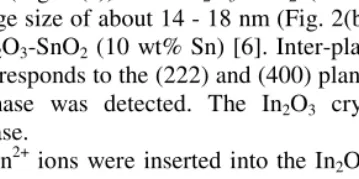
Fig. 2 shows TEM views of the samples. One may notice a non-uniform morphology and nanosized grain agglomeration (Fig. 2(a)). The In2O3-SnO2 (35 wt% Sn) nanocomposite has spherical-like
grains with an average size of about 14 - 18 nm (Fig. 2(b)), whereas an average size of about 12 nm was observed for In2O3-SnO2 (10 wt% Sn) [6]. Inter-planar spacing of about 0.29 nm and 0.25 nm
are found, which corresponds to the (222) and (400) plans of In2O3, respectively; hence, no evidence
crystalline SnO2 phase was detected. The In2O3 crystallites are therefore surrounded by an
amorphous SnO2 phase.
Thus, a part of Sn2+ ions were inserted into the In
2O3 lattice and other parts (in excess) formed
the SnO2 phase which remained amorphous. This result is in agreement with that obtained from
XRD analysis. In other works both In2O3 and SnO2 phase remained independent [4,7].
Fig. 2. (a) TEM image of the In2O3-SnO2 nanocomposite; (b) HRTEM image for 2 different interplanar spacing
patterns of In2O3
The AFM image (Fig. 3) shows that the roughness (rms) increases with the SnO2 content. The
rms increases from 10.8 nm for In2O3-SnO2 (10 wt% Sn ) to about 18.7 nm for In2O3-SnO2 (35 wt%
Sn) nanocomposite, indicating, at a first sight, that the active surface of the In2O3-SnO2 (10 wt% Sn )
nanocomposite becomes higher than that In2O3-SnO2 (35 wt% Sn ), presuming a high electric
response in presence of a reducing or an oxidizing gas.
Fig. 3. AFM image of (a) In2O3-SnO2 (10 wt% Sn) and (b) In2O3-SnO2 (35 wt% Sn) nanocomposite
3.3 Sensor response of the In2O3-SnO2 nanocomposite
We begin by studying the resistance behavior of In2O3-SnO2 nanocomposites in ambient flowing air
(without NO2) versus temperature. This study is of prime importance to point out the ability of the
sample to be used as a sensor. Figure 4 depicts the variation of the resistance of In2O3-SnO2
nanocomposites versus temperature under constant flowing air. It can be easily seen that the In2O3
-SnO2 (35 wt% Sn) nanocomposite is more resistive than the In2O3-SnO2 (10 wt% Sn ) film; on the
other hand the resistance increases while increasing Sn content, probably due to the presence of the amorphous SnO2 phase.
It is worth noting (Figure 4) that In2O3-SnO2 resistances nanocomposite decrease while varying
the temperature from ambient to 230 °C. It is well known that the value of the conductivity strongly depends on the nature of the predominant defects involved in the conduction mechanism (mainly oxygen defects in semiconducting oxides). On the other hand, defects and charge carriers may be activated by increasing the temperature leading to an increase of the conductivity.
50 100 150 200 250
103
104
105
106
107
108
109
In2O3-SnO2 (35 wt% Sn )
In2O3-SnO2 (20 wt% Sn )
In2O3-SnO2 (10 wt% Sn )
R
es
is
ta
nc
e
(
Ω
)
Temperature (°C)
Fig. 4. Resistance of the screen printed In2O3-SnO2 films measured at various operating temperatures in ambient
air.
As NO2 possesses the properties of an oxidant gas, in the present work, the sensor response of the
film was represented by S (%):
Where Ra is the resistance of the film in air and Rg is that upon exposure to NO2.
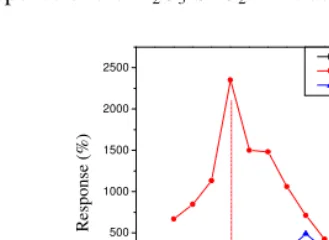
Figure 5 shows the response of the In2O3-SnO2 films as a function of the operating temperature.
120 140 160 180 200 220 240 260 280
0 500 1000 1500 2000 2500
R
es
po
ns
e
(%
)
Temperature (°C)
In
2O3-SnO2 (10 wt% Sn) In
2O3-SnO2 (35 wt% Sn) In2O3-SnO2 (20 wt% Sn)
Fig. 5. Effect of working temperature on the sensor response in presence of 100 ppm of NO2
According to Figure 5 we notice that the maximum of the response of the In2O3-SnO2 (10 wt%
Sn ) layer occurs at an operating temperature of about 180 °C, while the In2O3-SnO2 (20 wt% Sn and
35 wt%) nanocomposite exhibit a maximum at operating temperatures of about 200 °C and 160 °C, respectively. Therefore, one may note that the addition of a moderate quantity of SnO2 to the In2O3
increases the response and decreases the operating temperature for NO2 detection as already reported
with similar to nanocomposites [8].
4 Conclusions
In this work, the structural and morphological properties of a nanocomposite formed by crystalline In2O3 and amorphous SnO2 have been investigated. Subsequent to the increase of SnO2 content, grain
size, roughness (rms) and constant lattice ‘a’ increases. The nanocomposite-based sensor was found to be highly sensitive to NO2, as SnO2 content is optimized. It seems to be clear that the addition of a
moderate quantity of amorphous SnO2 to In2O3 (final Sn content = 35 wt%; final In content 65 wt %)
increases the response and decreases the operating temperature of the screen-printed layer. However, it should be noted that the addition of a random quantity (non-quantified) of SnO2 (exp: 20 wt% Sn )
could degrade the NO2 response and/or decrease the operating temperature.
References
1. Ting-Jen Hsueh, Cheng-Liang Hsu, Sens. Actuators, B131 572-576 (2008). 2. B. Bessaïs, N. Mliki, R. Bennaceur. Semicond. Sci. & Technol., 8 116-121 (1993). 3. Jaswinder Kaur, Rajesh Kumar, M.C. Bhatnagar, Sens. Actuators, B126 478-484 (2007). 4. Dewei Chu, Yu-Ping Zeng, Dongliang Jiang, Yoshitake Masuda, Sens. Actuators, B137
630-636 (2009).
5. A. Donato, F. Della Corte, M.Gioffrè, N.Donato, A.Bonavita, G.Micalli, G.Neri, Thin Solid Films, 517 (2009) 6184-6187.
6. H. Mbarek, M. Saadoun, B. Bessais, Sensor Letters, Vol. 6, 1-4, 2008.
7. Giovanni Neri, Anna Bonavita, Giuseppe Micali, Giuseppe Rizzo, Nicola Pinna, Markus Niederberger, Jianhua Ba, Sens. Actuators, B130 (2008) 222-230.