Electronic Thesis and Dissertation Repository
8-22-2012 12:00 AM
Delay Extraction Based Equivalent Elmore Model For RLC On-Chip
Delay Extraction Based Equivalent Elmore Model For RLC On-Chip
Interconnects
Interconnects
Shamsul Arefin Siddiqui
The University of Western Ontario
Supervisor
Dr. Anestis Dounavis
The University of Western Ontario
Graduate Program in Electrical and Computer Engineering
A thesis submitted in partial fulfillment of the requirements for the degree in Master of Engineering Science
© Shamsul Arefin Siddiqui 2012
Follow this and additional works at: https://ir.lib.uwo.ca/etd
Part of the Electrical and Electronics Commons, Systems and Communications Commons, and the
VLSI and Circuits, Embedded and Hardware Systems Commons
Recommended Citation Recommended Citation
Siddiqui, Shamsul Arefin, "Delay Extraction Based Equivalent Elmore Model For RLC On-Chip Interconnects" (2012). Electronic Thesis and Dissertation Repository. 748.
https://ir.lib.uwo.ca/etd/748
This Dissertation/Thesis is brought to you for free and open access by Scholarship@Western. It has been accepted for inclusion in Electronic Thesis and Dissertation Repository by an authorized administrator of
DELAY EXTRACTION BASED EQUIVALENT ELMORE MODEL
FOR RLC ON-CHIP INTERCONNECTS
(Spine title: Delay Extraction Based Elmore Model For On-Chip Interconnect)
(Thesis format: Monograph)
by
Shamsul Arefin Siddiqui
Graduate Program in Engineering Science Department of Electrical and Computer Engineering
A thesis submitted in partial fulfillment of the requirements for the degree of
Master of Engineering Science
The School of Graduate and Postdoctoral Studies The University of Western Ontario
London, Ontario, Canada
ii
CERTIFICATE OF EXAMINATION
Supervisor
______________________________ Dr. Anestis Dounavis
Supervisory Committee
Examiners
______________________________ Dr. Len Luyt
______________________________ Dr. Quazi Mehbubar Rahman
______________________________ Dr. Rajiv K. Varma
The thesis by
Shamsul Arefin Siddiqui
entitled:
Delay Extraction Based Equivalent Elmore Model
For RLC On-Chip Interconnects
is accepted in partial fulfillment of the requirements for the degree of Master of Engineering Science
iii
As feature sizes for VLSI technology is shrinking, associated with higher operating
frequency, signal integrity analysis of on-chip interconnects has become a real challenge
for circuit designers. For this purpose, computer-aided-design (CAD) tools are necessary
to simulate signal propagation of on-chip interconnects which has been an active area for
research. Although SPICE models exist which can accurately predict signal degradation
of interconnects, they are computationally expensive. As a result, more effective and
analytic models for interconnects are required to capture the response at the output of
high speed VLSI circuits. This thesis contributes to the development of efficient and
closed form solution models for signal integrity analysis of on-chip interconnects. The
proposed model uses a delay extraction algorithm to improve the accuracy of two-pole
Elmore based models used in the analysis of on-chip distributed RLC interconnects. In
the proposed scheme, the time of fight signal delay is extracted without increasing the
number of poles or affecting the stability of the transfer function. This algorithm is used
for both unit step and ramp inputs. From the delay rational approximation of the transfer
function, analytic fitted expressions are obtained for the 50% delay and rise time for unit
step input. The proposed algorithm is tested on point to point interconnections and tree
structure networks. Numerical examples illustrate improved 50% delay and rise time
estimates when compared to traditional Elmore based two-pole models.
Keywords
iv
There were many steps to take to complete this work. Each step would have been
impossible without the help of many people. First of all, I am deeply grateful to my
supervisor Dr. Anestis Dounavis of the Department of Electrical and Computer
Engineering, University of Western Ontario. I really appreciate him for introducing me
to the area of interconnect modeling and motivating me in this field of research. His
patience towards my project and friendly disposition has always had a positive effect on
my work. I really acknowledge his advice and guidance throughout my whole master’s
program.
I would also like to extend my thanks towards every faculty member, staff
member and friend of the Department of Electrical and Computer Engineering,
University of Western Ontario for their support and help at various stages of my thesis
work. I would like to specially mention my colleagues Sourajeet Roy, Amir Beygi and
Ehsan Rasekh for their invaluable advice.
Last but not the least; I would like to thank my parents, Mr. Abdur Rahman
Siddiqui and Mrs. Nargis Siddiqui and my wife Jisana Noorjahan for their continuous
v
Certificate of Examination……….…...ii
Abstract….……….………...iii
Acknowledgements..….……….………...iv
Contents ……….………....v
List of Figures ………viii
List of Tables………...x
Abbreviations………..xiii
1. Introduction………..1
1.1Background Review and Problem Identification……….1
1.2Objectives and Contribution………....6
1.3Organization of the Thesis………...7
2. Literature Review………8
2.1Introduction ………...………..8
2.2VLSI Interconnect with Physical and Electrical Parameters ………..………9
2.3 Introduction to Closed Form Interconnect Modeling…...……….12
2.4 Review of Closed Form RLC Interconnect………...14
2.4.1 Frequency Domain Representation of Transfer Function………...14
2.4.2 Elmore Delay Based Models (Single Pole Model)………17
2.4.3 Elmore Delay Based Models (Two Pole Lumped Model)……….20
2.2.4 Two Pole Distributed RLC Interconnect Model ….………..……26
vi
3.3.1 Extracting Time of Flight Delay…...……….29
3.3.2 Fitted Functions for f50%(,)and frise(,)………34
3.3 Proposed Model for Ramp Input ………...42
3.3.1 Time Domain Solution for Ramp Input…..………...42
3.3.2 Prediction of 50% Delay and Rise Time for Ramp Input………..45
3.4 Conclusion……….………....46
4. Numerical Examples………..……….47
4.1 Introduction…...………...…...47
4.2 Selecting Unit Step Input………...47
4.2.1 Example 1-Single Line Interconnect……….47
4.2.2 Example 2-Symmetrical Tree Structure Interconnect………53
4.2.3 Example 3-Unsymmetrical Tree Structure Interconnect ………..56
4.2.4 Summary of the Results……….59
4.3 Selecting Ramp Input……….………59
4.3.1 Example 1-Single Line Interconnect……….60
4.3.2 Example 2-Symmetrical Tree Structure Interconnect………..…..71
4.3.3 Example 3-Unsymmetrical Tree Structure Interconnect ………...75
4.3.4 Summary of the Results……….75
4.4 Conclusions………....…...……….75
5. Conclusions……….……….…...77
vii
viii
2.1 Interconnect and gate delay with IC technology evolution .…..………....10
2.2 Cross-section of a single-strip shielded transmission line…………..….………..11
2.3 Circuit Model for Single Line Interconnect………....……...13
2.4 Circuit Model Tree Structure Interconnects ……….………15
2.5 Circuit model of Elmore RC interconnect………..………...17
2.6 Circuit Model Elmore RC Tree Structure Interconnects..……….18
2.7 Lumped RLC Section for Equivalent Elmore Delay ...……….20
2.8 Circuit model for lumped RLC trees ………….……...……….………21
2.9 Time Scaled 50% delay versus …………...……...……….25
2.10 Time Scaled Rise Time versus …………...26
3.1 The time scaled 50% delay for different values of and ...…………...………..32
3.2 The time scaled rise time for different values of and ...…………...33
3.3 The time scaled 50% delay for different values of and (a) P=0.3 (b) P=4...44
4.1 Transient response of Example in 4.2.1 for 0.05cm line length……...49
4.2 Transient response of Example in 4.2.1 for 0.2cm line length………...50
4.3 Example of symmetrical tree structure………..53
4.4 Transient response of symmetrical tree structure of node N4...54
4.5 Transient response of unsymmetrical tree structure………..57
ix
4.8 Transient response of Example in 4.3.1. For ramp input of 0.1ns for 0.2cm of line
length……….….63
4.9 Transient response of Example in 4.3.1. For ramp input of 0.1ns for 0.5cm of line
length………..64
4.10 Transient response of tree structure of node N4 for ramp input of 0.05ns rise
time.………...69
4.11 Transient response of tree structure of node N4 for ramp input of 0.1ns rise
time………70
4.12 Transient response of unsymmetrical tree structure for ramp input of 0.1ns rise
x
2.1 Increasing clock speed in IC technology………...9
3.1 Coefficients of i,j,k ………..……...38
3.2 Coefficients of i,j,k ……….39
3.3 Coefficients of ir,j,k………..…….………...40
3.4 Coefficients of ir,j,k………..41
4.1 Single line interconnect parameters ..………....………48
4.2 Comparisons of 50% delay and rise time for single line interconnect of proposed model with conventional two pole model and HSPICE for unit step input. The line length is 0.05 cm (Example 4.2.1.………..…...51
4.3 Comparisons of 50% delay and rise time for single line interconnect of proposed model with conventional two pole model and HSPICE for unit step input. The line length is 0.2 cm (Example 4.2.1)...….……..………...……..52
4.4 Tree structure Interconnect lengths normalized to lx…...…….………...53
4.5 Capacitance normalized to Cx………...……….55
4.6 Comparisons of 50% delay and rise time for symmetrical tree structure interconnect of proposed model with conventional two pole model and HSPICE for unit step input. For tree example outputs are observed at node N4…………..55
4.7 Interconnect lengths normalized to lx for unsymmetrical tree structure...……56
xi
for unit step input. Outputs are observed at node N5 and Node N7..……….58
4.10 Comparisons of 50% delay and rise time for ramp response of 0.025ns of
proposed model with conventional two pole model and HSPICE. The line length
is 0.2 cm (Example 4.3.1)...………...65
4.11 Comparisons of 50% delay and rise time for ramp response of 0.025ns of
proposed model with conventional two pole model and HSPICE. The Line Length
is 0.5 cm (Example 4.3.1)…...………...………66
4.12 Comparisons of 50% delay and rise time for ramp response of 0.1ns of proposed
model with conventional two pole model and HSPICE. The line length is 0.2 cm
(Example 4.3.1)………..67
4.13 Comparisons of 50% delay and rise time for ramp response of 0.1ns of proposed
model with conventional two pole model and HSPICE. The Line Length is 0.5 cm
(Example 4.3.1)…...………...………68
4.14 Comparisons of 50% delay and rise time for symmetrical tree structure
interconnect of proposed model with conventional two pole model and HSPICE
for ramp input of 0.05ns. For tree example outputs are observed at node N4……71
4.15 Comparisons of 50% delay and rise time for symmetrical tree structure
interconnect of proposed model with conventional two pole model and HSPICE
xii
xiii
AWE ASYMPTOTIC WAVEFORM EVALUATION
CAD COMPUTER AIDED DESIGN
CFH COMPLEX FREQUENCY HOPPING
CPU CENTRAL PROCESSING UNIT
IC INTEGRATED CIRCUITS
MEMS MICRO ELECTRO MECHANICAL SYSTEMS
MNA MODIFIED NODAL ANALYSIS
ODE ORDINARY DIFFERENTIAL EQUATION
PDE PARTIAL DIFFERENTIAL EQUATION
PRIMA PASSIVE REDUCED ORDER INTERCONNECTS MACROMODELING ALGORITHM
PUL PER-UNIT-LENGTH
RC RESISTIVE-CAPACITIVE
RLC RESISTIVE-INDUCTIVE-CAPACITIVE
SPICE SIMULATION PROGRAM WITH INTEGRATED CIRCUIT EMPHASIS
VLSI VERY LARGE SCALE INTEGRATION
xiv
CMOS COMPLEMENTARYMETALOXIDESEMICONDUCTOR
MOS METALOXIDESEMICONDUCTOR
SSN SIMULTANEOUS SWITCHING NOISE
CHAPTER 1
INTRODUCTION
1.1
Background Review and Problem Identification
The process of creating integrated circuits by combining hundreds of thousands of
transistors into a single chip is usually referred to very-large-scale-integration (VLSI).
VLSI began in early 1970s when complex semiconductor and communication
technologies were being developed. Now a days, VLSI circuits and integrated circuit (IC)
chips find application in numerous fields like mobile and satellite communication,
computer hardware, micro-electromechanical systems (MEMS) devices, robotics and
other electronic systems. VLSI circuit density and complexity has exponentially
increased over the years leading to miniaturization of electronic systems, increase in
speed of production from circuit specifications to actual hardware development and a
resulting decline in prices of electronic devices. The rapid decrease in featured size has
followed by a commensurate increase in operating frequencies. At gigahertz range [1]
frequencies, design of clocks has been very critical which mainly determines the speed of
operation of such circuits. As anticipated by Moore’s law, the number of transistors in an
integrated circuit (IC) has doubled every two to three years. Modern ICs are now
composed of millions of transistors switching simultaneously within a fraction of a
At present, 32 nm technology is in production and microprocessor clock frequencies
are well above GHz range. The speed of an electrical signal in an IC is governed by two
components. The first component is the switching time of an individual transistor, known
as transistor gate delay, and the second one is the signal propagation time between
transistors, known as wire delay or interconnect delay. In modern VLSI circuits, major
challenges include layout optimization, high power dissipation at high frequencies of
operation, increased interconnect delays, crosstalk noise between mutually coupled
interconnects and simultaneous switching noise (SSN) in the power/ground plane pair. It
has been analyzed that signal integrity problems in interconnects determines the
performance of overall circuits. It is important to predict signal degradation like
propagation delay, crosstalk noise, signal overshoot, ringing and attenuation in the early
design cycles [2]-[5] which can critically affect system response. Using computer aided
design (CAD) tools for signal integrity, simulations have replaced the more
time-consuming and inefficient practice of circuit development and testing at every stage of
the design cycle for modern IC circuitry. However interconnect simulations suffer from a
myriad of issues which require sophisticated CAD tools for analysis.
In the past, interconnects were modeled as a single lumped capacitance. Then
lumped resistance-capacitance (RC) models were introduced in the analysis of the
performance of on-chip interconnects [6], [7]. However, the electrical length of
interconnects have become a significant fraction of the fundamental and harmonic
wavelength of the transient signal [8] at the gigahertz speed of operation with multiple
when dealing with these high speed interconnects. At such high speeds, interconnects
must be modeled as distributed resistive-inductive-capacitive (RLC) transmission lines as
opposed to lumped resistive-capacitive (RC) models to account for the non monotonic
nature of the response [9].
Since overall circuit performance depends on interconnect delay, low dielectric
metals like copper has been used in IC technology to decrease the line resistance and
capacitances [10]. However this does not significantly decrease the line inductances. This
has led to inductive line effects being a significant contributor to signal degradation. As
the inductive effect of the line becomes dominant, the propagation delay of the line
increases. Since feature sizes shrink in deep sub-micrometer technology to 90nm and
beyond, signal propagation delay in interconnect has been found to outweigh the gate
delay [10], [11]. This delay, if not effectively quantified can cause improper triggering
and timing uncertainty. Line inductance can also lead to effects like ringing and
non-monotonic response contaminated with spurious glitches on active lines.
As mentioned in the previous paragraphs, on-chip interconnects were modeled as
RC lines and single-pole Elmore-based models [6], [12]–[14] were most widely used to
estimate signal delay. However predicting signal waveform in tree structure interconnects
has been prime concern. Elmore based model is used as a delay model for the
buffer insertion in RC trees and wire sizing [15]-[24]. The popularity of this model
is due to the fact that it has analytic expression for predicting 50% delay and rise
time which is computationally fast and well suited for considering simulations of
limitations modeling RLC distributed interconnect networks, since these RLC lines may
give non monotonic responses. As a result modeling RLC interconnects for modern
circuit designers has been the centre of intense research [25]-[43]. To predict signal
transients in high-speed interconnects, the lines are modeled as single line, coupled line
and tree structure interconnects. In broad perspective there are mainly two ways to model
on-chip interconnects which are SPICE macromodels and closed-form analytic models.
SPICE is the most common simulation tool that generally uses numerical
integration or convolution techniques to provide accurate results. SPICE
macromodels include both lumped model and models based on delay extraction using
techniques such as method of characteristics [25]. The conventional lumped models or
rational approximation models (such as PRIMA [44], MRA [29]-[30], compact
differences [45]) represent interconnects as resistive, inductive and capacitive circuit
elements or as ordinary differential equations (ODE). However for high frequency
applications, the signal delay can be significant. These algorithms approximate the
propagation delay implicitly without using delay extraction. Nonetheless to model long
lines with significant delay these algorithms require higher order rational approximations
to accurately capture the delay of the signal leading to inefficient transient SPICE
simulation. For more compact class of models the method of characteristics [25] has
been used which is based on extracting the line-propagation delay [26]-[30] .Since the
delay terms can account for the high frequency characteristics of an interconnect, these
models allow more compact discretization of the line and lead to smaller matrices when
or method of characteristic algorithms requires numerical integration or convolution
techniques which obviously provide excellent accuracy but they are computationally
expensive to be used in layout optimization [23] since this requires simulating
circuit networks composed of millions of logic gates.
In order to avoid the computational complexity of SPICE simulations closed-form
analytic models have been developed. In order to derive closed form analytic models for
on-chip interconnects, far end transistor is modeled as parasitic capacitor and near end
transistor is modeled as resistor serially connected to a voltage source. These models are
usually effective for obtaining the far end solutions. Such circuit scenarios represent a
point-to-point interconnect system in IC designs ([16]-[24]) useful for initial design or
layout optimization cycles and use simple low order rational function to approximate the
transfer function so that it can be easily converted to the time-domain in a closed form
manner without requiring any numerical integration. Since these methods don’t use
numerical integration of large matrices they are computationally more efficient. Single
pole Elmore based RC model [12] was the first analytic closed form model for
on-chip interconnects. Considering the inductance effect of RLC interconnects, two
pole model (second order approximation) was developed in order to capture non
monotonic responses of RLC lines. To obtain more accurate models, multi-pole
transfer functions [12]-[14], [31]-[32], traveling-waveform technique [34]-[35], modified
Bessel function [37]-[40] and Fourier analysis [41] were introduced later on. However,
extending these techniques to efficiently analyze RLC tree structures is a challenging
Even though Elmore based models have limited accuracy, they are commonly used
to analyze integrated circuits composed of millions of gates, since it is often impractical
and time consuming to use accurate modeling techniques to evaluate the signal delay at
each node in the circuit . These techniques can provide quick relative delay estimates of
different paths in large circuit networks, allowing for more in-depth and time consuming
simulations to be performed on critical paths. The difficulty, in modeling inductive
dominant RLC interconnects is that these networks may exhibit significant signal delays.
Elmore based models rely on one or two pole approximations to estimate the delay. As a
result, it is extremely difficult to capture the delay of longer lines of interconnect. To
overcome this problem a new algorithm is proposed in this thesis.
1.2
Objectives and Contributions
The objective of this work is to use a delay extraction technique to improve the
accuracy of two-pole Elmore-based models for RLC interconnects. Since inductive
dominant RLC interconnects may exhibit significant signal delays, it is extremely
difficult to model these networks using only a two-pole transfer function. As a result, the
proposed algorithm provides a mechanism to explicitly model the signal delay caused by
RLC on-chip interconnect without significantly increasing the computational complexity
of the model.
The proposed delay extraction based equivalent Elmore model is derived from the
second order approximation of distributed RLC model since they provide better accuracy
is extracted without increasing the number of poles or affecting the stability of the
transfer function. This algorithm is used to obtain the far end time domain responses for
both unit step and ramp inputs. From this analysis, analytic fitted expressions are
obtained for the 50% delay and rise time for unit step inputs using curve fitting
techniques. The proposed algorithm is tested on point to point single line interconnects
and balanced and unbalanced tree structure networks. Numerical examples illustrate
improved 50% delay and rise time estimations when compared to traditional Elmore
based two-pole models.
1.3
Organization of the Thesis
The thesis is organized as follows. Chapter 2 reviews the challenges of
interconnect simulation in detail. Contributions made in literature to address these
problems are also reviewed with special emphasis on some of the latest closed form
models proposed. Chapter 3 deals with the proposed algorithms and shows the
development of this model. Extracting the time of fight signal delay, the model is
developed using the idea of second order approximation of distributed RLC model for
both unit step and ramp inputs. Using curve fitting techniques, analytic expressions are
provided for the 50% delay and rise time signals for unit step inputs. Chapter 4 deals with
several numerical examples (single line, balanced and unbalanced tree structures) to
proof the validity of the proposed model with HSPICE analysis and traditional two pole
model for both unit step and ramp inputs of different rise times. The thesis is concluded
Chapter 2
LITERATURE REVIEW
2.1 Introduction
There are many different technologies in which chips can be made but
complementary metal oxide semiconductor (CMOS) technologies are the most important
and common technologies for very large scale integrated (VLSI) applications such as
computers, digital signal processing, telecommunication, medical image processing,
cryptography and digital control systems. CMOS circuitry dissipates less power than
logic families with resistive loads. Since this advantage has increased and grown more
important, CMOS processes have become very popular and dominate, thus the vast
majority of modern integrated circuit manufacturing is on CMOS processes [46].
In a CMOS technology, doped silicon substrate is used to fabricate MOS device
with a gate of polysilicon on top of a thin layer of oxide. Then n+ or p+ doping is used to
make drain and source of the transistor. At first some voltage is applied to gate in order to
create the channel between source and drain. Then voltage is applied at the drain terminal
As a result, current flows from drain to source. In order to interconnect transistors, a stack
of metal layers is available to the designer. Lower level metal layers have higher
resistance values and upper level metal layers have lower resistance values. Also the
parasitic capacitances and inductances of on-chip interconnect vary from one metal layer
As Moore’s law predicts, the number of transistors in an integrated circuits (IC)
will double every two to three years. For over 30 years, the feature size of CMOS
technology has shrunk to dimensions into the nanometer region. According to
International Technology Roadmap for Semiconductors (ITRS) [47], [48], feature sizes
will further decrease at the rate of 0.7x per generation [1]. As a result of this continuous
scaling, higher circuit speeds, lower power and larger packing densities of transistors are
achieved. At present, Intel has started producing 32 nm technology microprocessor with a
clock frequencies of well above GHz. The speed of an electrical signal in an IC depends
on transistor gate delay (i.e. switching time) and the interconnect delay. Since
interconnect delay is more important that switching delay, modeling of on-chip
interconnects have been an intense area for research.
2.2 VLSI Interconnect with Physical and Electrical Parameters
As technology is scaled, interconnect delay starts to dominate the gate delay
which is shown in Fig. 2.1. Because of high operating frequencies and technology shrink
inductance effect can no longer be ignored. Inductance is a physical property of a closed
current loop. Inductive coupling can occur over a long distance, whereas capacitive
INCREASING CLOCK SPEED IN ICTECHNOLOGY
Year Technology (nm) Maximum Clock Speed (GHz)
2004 90 4
2007 65 6.7
2010 45 11.5
2013 32 19.3
coupling is limited to adjacent interconnects. As a result, it is not straightforward to
extend the existing parasitic extraction approach to perform inductance extraction in
on-chip interconnects.
Interconnects in VLSI and integrated circuits can be considered as strip lines or
microstrip transmission lines. For microstrip lines it consists of a conductive strip of
controlled width on a low-loss dielectric material mounted on a conducting ground plane.
Microstrip is by far the most popular structure, especially for VLSI and other integrated
circuits. The major advantage of microstrip is that all active components can be mounted
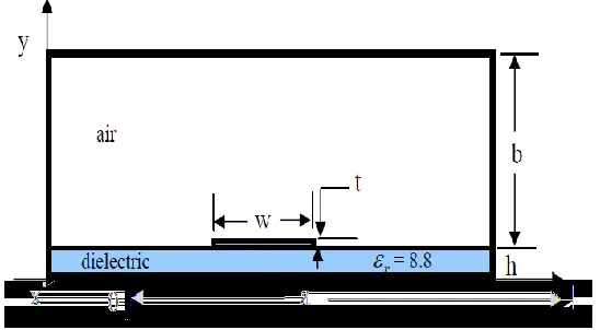
on top of the board. The physical structure of such interconnect is shown in Fig. 2.2
where w, t, h are the interconnect width, height (or thickness), inter-layer dielectric
thickness respectively. Interconnect width, height and length can be controlled by the
circuit designer. Transmission lines are best described by Telegraphers equation where
per unit length resistance, inductance and capacitance (R , L ,C) are needed. From the
physical design of interconnect structures it is important to extract the electrical
parameters of the interconnect in terms of per unit length resistance (R), capacitance (C)
and inductance (L) before performing the timing analysis in the design flow. In standard
cell design, quick interconnect parasitic extraction and delay estimation are done at the
place and route stage for optimum placement. These extraction becomes important since
the interconnect design affects every stage of the design flow.
There are usually two ways to extract interconnect electrical parameters from
their physical parameters. One is analytical expressions which are fast to calculate and
another way is to use field solver [49], [50]. Analytical expressions of the interconnect
per unit length resistance and capacitance are given by following equations [51] for the
structure shown in Fig 2.2
tw l R
(2.1)
h t t
h l
C 0r ( 0.5 )0r )
/ ln(
2
. (2.2)
where 0 and rare dielectric constant, and relative permittivity respectively. The
interconnect inductance equation is from the predictive technology model [52]
l t w t
w l l
L ln 2 0.5 0.22( )
2
0
(2.3)
where µ0is the permeability in free space.
Another approach for determining the per unit length parameters is to use 2-D and
3-D electro-magnetic field-solvers [50], [53]. In HSPICE the physical parameters of
interconnect based on latest technology can be given to extract the electrical R, L, C
parameters. Field solver provides better accuracy when compared to analytical formulas
at the expense of computational complexity. Once the electrical parameters are identified,
it is necessary to develop a model to estimate the delay. There are several closed form
interconnect models which have been developed over the years. Next section will discuss
some of those closed form models.
2.3 Introduction to Closed Form Interconnect Modeling
Analysis of on-chip interconnects are based on either simulation techniques or
closed-form analytic formulas. When it comes to modeling of on-chip interconnects for
signal integrity verification, the most important difficulty is the numerical integration
problem. This is because the distributed interconnects are best described by Telegraphers
partial differential equations which can provide an exact transfer function for the far end
response in the frequency domain only. However it does not have an exact time domain
representation. To provide an accurate time domain representation, numerical integration
techniques [54] are required at every time step. Simulation tools such as SPICE use
numerical integration or convolution techniques at every time step to provide accurate
results. However, these techniques are computationally expensive to be used in layout
For an iterative layout design of densely populated integrated circuits composed
of hundred millions of gates, accurate analytic models are needed to efficiently predict
the delay and rise times of interconnects. One of the traditional methods was to express
the frequency domain transfer function of interconnects as a simple rational function
which could then be converted to poles and residues form [12]-[14], [31]-[33]. As poles
and residues have a direct representation in the time domain, the interconnect response
can now be evaluated without numerical integration at every time step. Using this idea,
on-chip interconnects were analyzed as single-pole Elmore-based RC models [6],
[12]-[14] to estimate signal delay at early stages. In current integrated circuit designs, wire
inductance can no longer be ignored due to higher operating speeds and longer electrical
line lengths. Thus, analytic RLC interconnect models are required to efficiently
characterize the signal responses of today’s high-performance integrated circuits.
All of the above factors contribute to make on-chip interconnect modeling highly
challenging. Closed form models are important because of their simplicity while
maintaining reasonable accuracy as compared to SPICE. The next section deals with
various closed form models proposed in the literature.
Fig. 2.3: Circuit Model for Single Line Interconnect
+
-Vin
Rs
R, L, C
2.4 Review of Closed Form RLC Interconnect Models
2.4.1
Frequency Domain Representation of Transfer Function
The analysis of on-chip RLC interconnects starts with Telegraphers equation in
frequency domain. All closed form RLC models assume a quasi-TEM mode of signal
propagation. This means that the effect of imperfect line conductors and inhomogeneous
surrounding medium resulting in a component of the mutually transverse electric and
magnetic fields along the line axis is considered negligible [3]. The Telegrapher's
equations are a pair of linear differential equations which describe the voltage and current
on a transmission line with distance and time. The equations come from Oliver Heaviside
who in the 1880s developed the transmission line model. These equations are [55]
R sL
I(x,s) s)V(x,
x
I(x,
s)
sCV
(
x,
s
)
x
(2.4)
where s is Laplace transform variable, x is the position variable; V(x,s) and I(x,s)
represent the voltage and current of the transmission line respectively in the frequency
domain; R, L and C are the per-unit-length resistance, inductance and capacitance
respectively. The per unit length conductance G is assumed to be negligible for on-chip
interconnects. The solution of (2.4) can be expressed using the exponential matrix as
I(0,s)
s) V(0, e
s) I(l,
s)
V(l, Φl
where 0 Y Z 0
Φ (2.6)
Z=R+sL, Y=sC and l is the length of the transmission line. The exponential matrix of (2.5)
can be expressed using the cosh and sinh functions as shown below [55]:
s I s V ) ZY (l cosh ) YZ l sinh Y -YZ l sinh Y ) ZY l cosh( s l I s l V 0 -1 0
(0, )
) , 0 ( ( ) ( ) , ( ) , ( (2.7)
where Y0 Y( YZ )1. Now we look the circuit network for a RLC interconnect line
which is shown in Fig. 2.3. This represents a point-to-point interconnection driven by a
transistor (modeled as voltage source Vin serially connected to a linear resistanceRs) and
connected to the next gate (modeled as a capacitanceCl) and is commonly used in VLSI
design theory [17]-[30]. Considering this interconnect circuit as shown in Fig. 2.3, the
boundary conditions are represented as
Vin
+
-Rs C5 C6 C7 C8 C9 N7 l0 N0 N6 N3 N5 N2 N1 N9 N4 N8 l3 l1 l2 l5 l6 l7 l8 l9Vin V(0,s)RsI(0,s) (2.8)
V(l,s)sClI(l,s) (2.9)
Using (2.7)-(2.9), the far end transient response of single line interconnect can be
described as ) sinh( ) ( ) cosh( ) 1 ( 1 0
0
Y sC Y R C sR V V l s l s in
f (2.10)
where (l YZ).
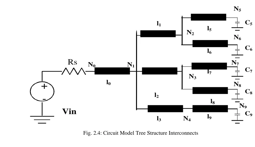
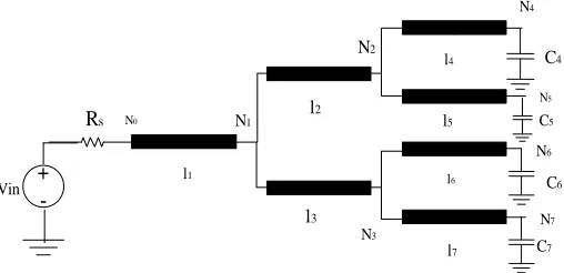
Figure 2.4 shows an example of a distributed RLC tree which is often used to
analyze clock distribution networks. In that example, a driver with an output resistance is
Rs connected to the root of the tree N0. All of the output nodes (N5…..N9) are called leaves
and connected with load buffers which can be used to drive the RLC trees in the next
level. The load buffers are modeled by capacitors. All of the branches in the tree are
represented by distributed RLC lines. The tree can be balanced or unbalanced; but
unbalanced trees exhibit more complex characteristics than balanced trees [41].
The output voltage Vouti from the voltage source to a certain node Ni is [41],
k k k Lk k
L d L in i out Z Z Z R Z V V )) sinh( ) / ( ) cosh( 1 , , 0 0 , 0 , (2.11)
where k and Z0,k are the propagation operator and characteristic impedance of the k th
following each branch in the path from node N0 to Ni. If node Nj branches out to a single
interconnect k (such as nodes N4 of Fig. 2.4), then the input impedance ZL,j is defined as
k k
L k k
k k
k k
L k j L
Z Z
Z Z
Z Z
sinh cosh
sinh cosh
, ,
0
, 0 ,
, 0
, (2.12)
If node Nj branched out to multiple interconnects (such as node N1 of Fig. 2.4), then the
input impedance ZL,j at node Nj is the parallel combination of the input impedances of
the downstream branches which are connected to node Nj.
These transfer functions of single line and tree structure interconnect (2.10),
(2.11) have no direct representation in the time domain and thus real-time prediction of
delay of RLC interconnects. Various closed form models [12]-[14], [31]-[41] were
developed to provide efficient representation of (2.10)-(2.12) in time domain and will be
now discussed.
2.4.2
Elmore Delay Based Models (Single Pole Model)
One of the earliest and popular models for SI verification in interconnects was the
Elmore delay based models as proposed in [12]. For ease of presentation without loss of
R
Vin C
Rs
Cl
+
CT Vin
+
generality, each interconnect is explained as simple lumped RC circuits as shown in Fig.
2.5. This model is commonly used in VLSI design theory [17]-[30].
Transfer function of such RC circuit is given by
) 1
( 1 )
(
T TC sR s
H
(2.13)
where RT =Rs+R and CT =Cl+C are the total interconnect resistances and capacitances
respectively which includes sources resistance and load capacitance. Now if the input is a
unit step function, then the time domain solution is given by
) / exp( 1
( )
( D
out t t T
V
(2.14)
where TD represents the time constant which is RT CT.
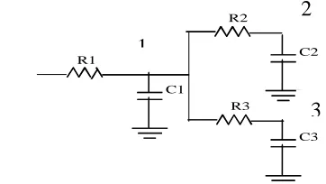
Elmore model is particularly appealing for tree structure interconnects where each
interconnect in tree structure is considered as lumped RC circuits which is shown in Fig.
2.6. The transfer function of such tree structure at node i is given by
) 1
(
1 )
(
k ik kR C s s
H (2.15)
R1
C1
R3
C3 C2
Fig. 2.6: Circuit Model Elmore RC Tree Structure Interconnects
1
where k is the index that covers every capacitor in the circuit; Rik is the common
resistance respectively, from the input to the node i and k [12],[56]. This first-order
approximation matches the first moment of the transfer function at node i but
approximates the higher-order moments by
i
k ik k
i C R
m
(2.16)as seen by the expansion
... 1 ... 1 ) ( 2 2 2 2
1
k ik k k ikkR s C R
C s s m s m s H (2.17)
Elmore model is basically single pole model (first order approximation).There is a simple
closed-form solution for the time constant
i D
T for the tree shown in Fig. 2.6. The time
constant at node i is given by
k ik k
D C R
T
i (2.18)
The equation of 50% delay for unit step input becomes
t50% 0.693TD (2.19)
Since, the delay of an exponential function of (2.14) is well defined and easy to
analyze, this model was very popular among circuit designers. However, this model does
not consider inductance effect which is very obvious when modern switching speeds
monotonic due to the large line inductances. For such cases instead of RC model, RLC
models (two pole) or even multi-pole models are required.
2.4.3
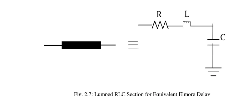
Equivalent Elmore Delay Model (Two Pole Lumped Model)
The transfer functions of (2.10) and (2.11) include hyperbolic functions of the
complex frequency variable s and do not have a direct representation in the time domain.
This makes it difficult to analytically predict the signal delay of interconnect networks.
As a result the extension of equivalent two-pole Elmore delay models for RLC tree
networks is developed in [42]-[43],[56]. For the case of two pole lumped model [56],
single line interconnect is represented as lumped resistive-inductive-capacitive (RLC)
elements as shown in Fig. 2.7. As a result, the circuit of Fig. 2.7 has second order transfer
function which is given by
1 1
)
( 2
RCs LCs
s
H (2.20)
R
L
C
This transfer function is expressed in terms of its damping factor and natural
frequency n as
2 2
2
2 )
(
n n n
s s
s H
(2.21)
where
LC RC
2
&
LC n
1
(2.22)
The poles of the transfer function of (2.21) are
1( 2
2 ,
1 n
P (2.23)
R5 L5
C5 R1 L1
C1
Vin
R3 L3
C3 R2 L2
C2
R4 L4
C4
R6 L6
C6
R7 L7
C7 N1 N1
N
2N3
N4
N5
N
6N7
For the case of tree structure network, each interconnect in the tree is modeled as
lumped resistive-inductive-capacitive (RLC) elements, as shown in Fig. 2.8. Typically,
moment matching techniques are used to express the transfer functions of this tree
structure interconnect as a power series [43]
2 2 1 2 2 1 1 1 1 ) ( s b s b s m s m V V s H in out
(2.24)
where the moments mj are
( ), 1,2,.... !
1
j ds s H d j m j j
j (2.25)
and
b1 m1 2 2 1
2 m m
b (2.26)
The first two moments of this tree network at node Nj can be calculated using the
following simple closed-form expressions [56] where first moment is similar to equation
(2.16) of RC circuit of Fig. 2.8.
k ik k i R Cm1 (2.27)
k ik k k ik k i L C R C m 2where k is the index that covers every capacitor in the circuit; Rik and Lik are the
common resistance and inductance, respectively, from the input voltage node to node Ni
and Nk [56].
For the general RLC tree shown in Fig. 2.8, the voltage drop at any node as Ni
compared to the input voltage is
k
ki ki k
k i
in s V s CV s s R L s
V ( ) ( ) ( ) ( ) (2.29)
If the input is a unit impulse, Vin(s)is equal to 1.0 and the voltages at the nodes of the tree
are the unit impulse responses of these nodes. Thus, the normalized transfer function gi(s)
at node Niof tree structure is given by Vi(s)and is
k
kI ki k
k
i s C V s s R L s
g ( ) 1 ( ) ( ) (2.30)
Using the moment matching techniques
i n
and iat this transfer function of node Ni of
general tree structure is given by
k ik k k
ik k
i
L C
R C
2
&
k ik k ni
L C 1
(2.31)
The time constants RC and LC in single line structure are replaced by the summations
Once the transfer function of single line or tree structure interconnect is obtained
in the form of damping factor and natural frequency, the time domain response of (2.21)
for a step input with supply voltage of VDD is given by
1 1 1 2 ) ( 2 ) 1 ( 2 ) 1 ( 2 2 2 n n t t DD DD n out e e V V t
V (2.32)
where tn is a dimensionless time variable defined as tn tn. The output voltage of (2.32) is a nonlinear function with respect to the variable . As a result, an analytic
formula is not directly available for the 50% delay since the solution of (2.32) is obtained
iteratively using methods such as Newton-Rhapson’s method. For this reason, (2.32) is
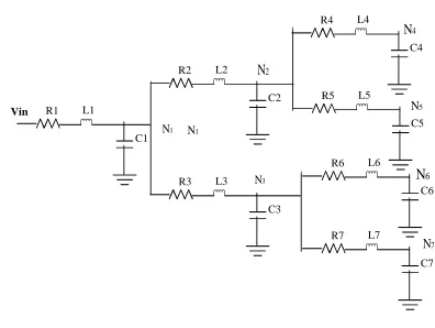
solved for various values of by setting Vout to 0.5VDD and solving for tn. Fig. 2.9 plots
the time scaled 50% delay for various values of . The results of this analysis are stored
and fitted to the following functions [56]
t50% (1.047e/0.851.39)/n (2.33)
where t50% corresponds to 50% delay with respect to time t. This equation is like the extension of 50% delay of single pole Elmore model of (2.19) considering inductance
effect of the interconnect. Equation (2.32) can also be used to calculate the rise time by
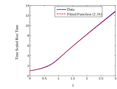
setting Vout to 0.1VDD and 0.9VDD and solving tnfor different values of . Fig. 2.10 plots
the time difference of Vout to reach 0.1VDD to 0.9VDD. Similar fitted expressions can also
So the expression of rise time is given by [56]
tr (6.017e1.35/0.4 5e1.25/0.64 4.39)/n (2.34)
where tr corresponds to the rise time.
2.4.4 Two
Pole Distributed RLC Interconnect Model
The exact transfer function of single line and distributed RLC trees are hyperbolic,
but very complicated. In [43], the accuracy of the two pole model is improved by directly
approximating the distributed hyperbolic functions of (2.10) and (2.11) as a power series
2.9: Time Scaled 50% delay versus
0 0.5 1 1.5 2 2.5 3
1 1.5 2 2.5 3 3.5 4 4.5
Data
Fitted Function(2.33)
Time Sca
led
50%
D
2 4 2 2 2 2 ) ! 4 1 ! 2 1 ( ! 2 1 1
coshk RkCklks LkCklk RkCklk s (2.35)
2 5 2 3 3 3 2 , 0 ) ! 4 1 ! 3 2 ( ) ! 3 1 ( sinh s l C R l C L R s l C R l L l R Z k k k k k k k k k k k k k k k k (2.36)
0,1 2 3) 2
! 3 1 (
sinh C l s C R l s
Zk k k k k k k (2.37)
to convert the transfer function to the form of (2.24) as
2 2 1 1 1 ) ( s b s b s H (2.38)
Fig. 2.10: Time Scaled rise time versus
0 0.5 1 1.5 2 2.5 3
0 2 4 6 8 10 12 14 Data
Fitted Function (2.34)
Time Sca
led
R
where
2 1 2 b
b
&
2
1
b n
(2.39)
In [43], it is shown that the Maclaurin series approximation from (2.35)-(2.37) to
obtain the moments of the transfer function of (2.38) are more accurate than the moments
calculated from the lumped model since the distributed RLC model are directly derived
from the hyperbolic functions of (2.10) and (2.11). Once the transfer function of (2.38) is
derived the fitted expressions of (2.33) and (2.34) can be used to analytically calculate the
50% delay and the rise time.
Elmore based models such as the fitted expression of (2.33) & (2.34) are widely
used in VLSI circuit design for fast delay estimation due to its computational efficiency.
However, the accuracy of Elmore models is limited since two poles may not be accurate
enough to capture the high frequency effects and signal delays of RLC lines. The next
chapter provides a methodology to improve Elmore based two pole model of RLC
Chapter 3
Delay Extraction Based Equivalent Elmore Model
For RLC On-Chip Interconnects
3.1 Abstract
In this chapter a delay extraction algorithm is utilized to improve the accuracy of
two-pole Elmore based models used in the analysis of on-chip distributed RLC
interconnects. In the proposed scheme, the time of flight signal delay is extracted without
increasing the number of poles or affecting the stability of the transfer function. This
algorithm is used for both unit step and ramp inputs. From the analysis, analytic fitted
expressions are obtained for the 50% delay and rise time for unit step input. For ramp
input, a lookup table can be created for the 50% delay and rise time. Since the time of
flight delay is extracted from the transfer function, the proposed algorithm provides a
mechanism to improve the accuracy of two-pole Elmore-based models without
significantly increasing the computational complexity.
Elmore based models rely on one or two-pole transfer functions to estimate the
delay. As a result, these approximations are not capable of capturing the early transient
responses required for predicting long signal delays and rise times caused by inductive
dominant on-chip interconnects.The proposed model basically extends the concepts of
two pole model [43], [56] to obtain the time domain analysis for any balanced and
function is obtained analytically in terms of predetermined coefficients and the per unit
length parameters. As a result, the proposed model provides a mechanism to improve the
accuracy for cases when inductive effects are significant, length of the line increases or
when rise time of the signal becomes sharper. The algorithm is used for various single
and tree structures interconnect scenarios for both unit step and ramp inputs.
The organization of the chapter is as follows: Section 3.2 develops the proposed delay
extraction based equivalent Elmore model for unit step input. Analytic fitted expressions
have been obtained for calculating 50% delay and rise time. Then the model is extended
for ramp inputs in section 3.3 where prediction of 50% delay and rise time has also been
discussed.
3.2 Proposed Model for Unit Step Input
Even though Elmore based models have limited accuracy, they are still commonly
used to analyze integrated circuits composed of millions of gates, since it is often
impractical and time consuming to use accurate modeling techniques to evaluate the
signal delay at each node in the circuit The objective of this work is to use a delay
extraction algorithm to improve the accuracy of this Elmore-based models for RLC
interconnects.
3.2.1 Extracting Time of Flight Delay
As illustrated in chapter 2, moment matching techniques are used to express the
2 2 1 1 1 ) ( s b s b s H
(3.1) Equation (3.1) usually refers to Elmore based two pole model. The proposed algorithm
uses a delay extraction based rational approximation to improve the accuracy of (3.1).
The first two moments of (3.1) are calculated using the same conventional moment
matching techniques such as the methodologies described in section 2.4.3 and 2.4.4. In
this paper, the procedure outlined in [43] is used since the hyperbolic approximations of
(2.35)-(2.37) were shown to be more accurate than the lumped model moment
calculations of (2.27)-(2.28). Once, the moments of the transfer function are calculated,
the time of flight delay Td is extracted from (2.21) as proposed in [57] to obtain
2 2 2 2 2 2 5 . 0 1 ) ( n n sT d d n s s e T s sT s H d (3.2)where 1sTd 0.5s2Td2 corresponds to a Maclaurin series approximation of esTd. The
delay operator esTd ensures that the voltage at the far end appears only after the
time-of-flight delay Td. Furthermore, the Maclaurin series approximation of esTd only changes
the numerator of (3.2) and does not increase the number of poles or affect the stability of
the transfer function. For the interconnect network of Fig. 2.3, a lower bound estimate of
the time of flight delay is
Td l LC (3.3)
estimate of the amount of delay that should be extracted from (3.2), since the voltage
signal at the far end can only appear after Td delay has occurred with respect to the input
voltage at the near end [57]. For the interconnect tree network of Fig. 2.4, a lower bound
estimate of the time of flight delay at node Niis calculated as a summation of propagation
delay of lossless lines as
k k k k id l L C
T (3.4)
where k is the index following each branch in the path from node N0 to Ni. The time
domain response of (3.2) corresponding to a step input with supply voltage of VDD can be
expressed as
Vout(tn) VDD 1 K1e tn( 2 1) K2e tn( 2 1)u(tn)
(3.5) where ) 1 )( 1 ( 2 ) 1 ( 5 . 0 ) 1 ( 1 2 2 2 2 2 2 1
K (3.6)
) 1 )( 1 ( 2 ) 1 ( 5 . 0 ) 1 ( 1 2 2 2 2 2 2 2
K (3.7)
The coefficient u(tn) is the unit step response, tn (tTd)n and Tdn. The
the equation of (2.32).
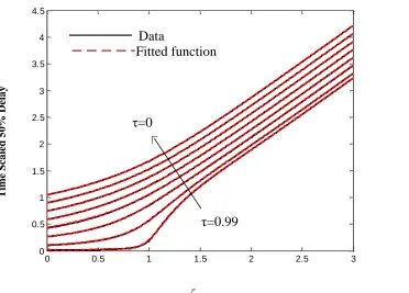
To calculate the 50% delay requires solving the nonlinear function of (3.5) for
specific values of and . Fig. 3.1 shows the solution of (3.5) for various values of
and by setting Vout to 0.5VDD and solving for tn. The results of this analysis can be
stored or fitted to some function to obtain quick estimates of the 50% delay. Let the fitted
function be defined as f50%(,). Thus, the 50% delay with respect to time t can be
calculated as
n d
f T t
, ) ( % 50 %
50 (3.8)
Note, when the time of flight delay is not extracted (i.e. 0), the fitted expression of
) , ( % 50
f will give similar 50% delay predictions as (2.33).
0 0.5 1 1.5 2 2.5 3
0 0.5 1 1.5 2 2.5 3 3.5 4 4.5
Data
Fitted function
τ=0
τ=0.99
Fig. 3.1 The time scaled 50% delay for different values of and
T
ime Sca
led 5
0
%
Dela
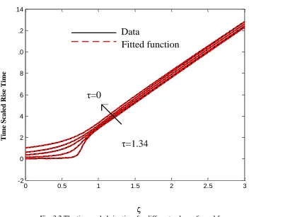
Equation (3.5) can also be used to calculate the rise time by setting Vout to 0.1VDD
and 0.9VDD and solving tn for different values of and . The results of this analysis
are shown in Fig. 3.2 which plots the time difference of Vout to reach 0.1VDD to 0.9VDD.
Let the fitted function for the rise time be defined as frise(,). Thus the rise time with
respect to time t can be calculated as
n rise rise
f t
, ) (
(3.9)
Section 3.2.2 discusses how f50%(,) and frise(,) are fitted to the data values of Fig.
0 0.5 1 1.5 2 2.5 3
-2 0 2 4 6 8 10 12 14
τ=0
τ=1.34
Data
Fitted function
Fig. 3.2 The time scaled rise time for different values of and
T
ime Sca
led
R
is
e
T
3.1 and Fig. 3.2, and how these functions are used to calculate the 50% delay and rise
times.
3.2.2 Fitted Functions for
f50%(,)and
frise(,)The numerical solutions for the 50% delay is fitted to rational functions for
specified ranges of as
1 0 99 . 0 9 . 0 / 9 . 0 8 . 0 / 8 . 0 6 . 0 / 6 . 0 4 . 0 / 4 . 0 2 . 0 / 2 . 0 0 / ) , ( 6 6 5 5 4 4 3 3 2 2 1 1 % 50 D N D N D N D N D N D N
f (3.10)
where Ni and Di are defined as polynomials with respect to ,
4 4 , 3 3 , 2 2 , 1 , 0
, i i i i
i
i a a a a a
N
Di bi,0 bi,1 bi,2 2 3 (3.11)
and ai,j and bi,j are polynomials with respect to ,
, ,3 3
2 2 , , 1 , , 0 , ,
,j i j i j i j i j i
a
, ,3 3
2 2 , , 1 , , 0 , ,
,j i j i j i j i j i
b (3.12)
The coefficients of i,j,k and i,j,k are listed in Table 3.1 and Table 3.2. The curve fitting