Design and Development of Coax-Fed Electromagnetically Coupled
Stacked Rectangular Patch Antenna for Broad Band Application
Manotosh Biswas1, * and Mausumi Sen2
Abstract—In this article, a set of closed-form expressions is proposed to predict the resonant frequency, quality factor, input impedance, bandwidth efficiency, directivity and gain for a coax-fed electromagnetically coupled stacked rectangular patch antenna. The computed results obtained with the present model are compared with the experimental and HFSS simulated results. The present model shows less error against the experimental and simulated results.
1. INTRODUCTION
Today, microstrip patch antennas are installed in portable wireless equipments, aircraft radomes, missiles, satellites and various radars [1]. Microstrip patch antennas possess many advantages such as low profile, light weight, small volume, and easy implementation. However, due to their resonant behavior, they radiate efficiently only over a narrow band of frequencies, with bandwidths typically only a few percent (about 5%) [2]. Due to this inherent limitation, the patch antenna is the major obstacle that restricts wide applications. Various radars and telecommunication systems employ multiband (broad bandwidth) characteristics. Therefore, the design and development of broad-band techniques are very important to enhance the bandwidth of microstrip antennas.
While maintaining the advantages of conventional single patch microstrip antennas, microstrip antennas of stacked configurations, consisting of one or more conducting patches parasitically coupled to a driven patch, overcome the inherent narrow bandwidth limitation by introducing additional resonances in the frequency range of operation, achieving bandwidths up to 6–20%. In addition, stacked microstrip configurations have achieved higher gains and offer the possibility of dual-frequency operation [3]. Today, the stacked patch antennas are used in radars, mobile, satellites, UHF RFID, MIMO and reconfigurable antennas [3–14]. Thus, the accurate computation of resonant frequency, input impedance, quality factors, bandwidth and gain of stacked patch antenna is very important to install properly in wireless equipments.
Stacked patch antennas have been investigated by several researchers reported in [15–24]. Among them, most of the articles [15–20] are experiment based, and some of the articles [21–23] are based on numerical methods. The useful parameters of a probe-fed electromagnetically coupled stacked rectangular patch antenna (PFEMCSRPA) are computed by numerical techniques [21–23] and also by commercial software [25]. The numerical methods are rigorous and computationally slow. So, they are not suitable for the design oriented interactive computer-aided design (CAD) for the direct synthesis of PFEMCSRPA. The CAD oriented conformal mapping, cavity model and single resonant parallelL-C-R
circuit are ideal for design purpose because it is very simple, easy to analysis, takes less computational time and can be directly applied to the CAD programs.
Received 21 April 2017, Accepted 17 September 2017, Scheduled 14 October 2017 * Corresponding author: Manotosh Biswas ([email protected]).
To the best of our knowledge, only one article [24] is available in open literature which provides the closed form expressions. However, this model has some drawbacks: (i) the lower cavity is treated as an uncovered patch, but the lower cavity is actually a patch covered with dielectric layer [26]; (ii) the fringing field effect, i.e., the effective patch lengthb1eff of lower patch has not been considered, but the fringing field effect very much depends on relative characteristics of substrates and dielectric cover layers [27]; (iii) it considers both the patches with the same ground plane, but the lower patch is treated as ground plane of upper patch [26]; (iv) it studies only the resonant frequency; (v) the design guideline has not been presented for quality factor, efficiency, directivity, gain and input impedance; and (vi) it has not considered the coupling between lower and upper patches.
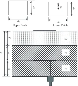
We have addressed these problems and proposed a simple model based on conformal mapping, cavity model and single resonant parallel L-C-R circuit to predict accurately the resonant frequency, input impedance, quality factor, efficiency, directivity and gain for a PFEMCSRPA as shown in Fig. 1. This model is very simple, efficient, fast and employs fewer mathematical steps. Microstrip is an old topic. So, we have employed an old theory for developing the present model. Though the present model employs the old theory or model, it is very efficient to overcome the disadvantages of the previous closed form model [24]. This efficient model is capable of predicting accurately above characteristics for wide range of variations of antenna, substrate and superstrate geometric and electrical parameters.
a2
b2 ρ
a1
b1
Upper Patch Lower Patch
Figure 1. Geometry of probe-fed stacked rectangular microstrip patch antenna.
The expressions for this model are introduced in Section 2. Section 3 includes the experimental tests. In Section 4, we present the predicted, measured and simulated results.
2. THEORY
lower patch. The lower and upper cavities have their own resonances, and they are in parallel [3].
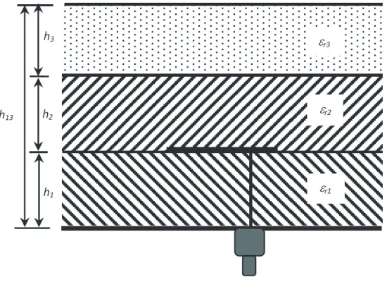
2.1. Lower Cavity
The lower cavity is analyzed as a rectangular patch in multi-dielectric layers [26] as shown in Fig. 2.
Figure 2. Geometry of lower cavity.
2.1.1. Effective Permittivity
When a patch is in multi-dielectric layers, the fringing field between the patch and ground plane is changed, and this effect is accounted for by the effective permittivityεr,eff1. The effective permittivity for this structure (Fig. 2) is obtained as [28, 29]:
εr,eff1=εr1p1n+εr1(1−p1n) 2
×
ε2
r2p2np3+εr2εr3
p2np4+ (p3+p4)
2
ε2r2p2np3p4+εr1(εr2p3+εr3p4) (1−p1n−p4)2 +εr2εr3p4
p2np4+{p3+p4} 2
(1)
where, p1n, p2n, p3 and p4 are the dielectric filling fractions. The derivation of εr,eff1 and the computational details of these filling fractions are presented in Appendix A.
2.1.2. Effective Patch Length
The effective patch length b1eff is defined as
b1eff =b1(1 +qb1)1/2 (2) here, qb1 is the fringing field factor which strongly depends on the relative characteristics of substrate and superstrates.
Theqb1 for this structure is obtained from [30] as
qb1 = v1+v2+v3+v4 (3)
v1 = 0.882
h1
b1
(4)
v2 = 0.164
(εr−1)
ε2 r
h1
b1
(5)
v3 =
(εr+ 1) [0.758 + ln (b1/h1+ 1.88)]
πεr
h1
b1
v4 =
h1
b1
(0.268εr+ 1.65) (7)
εr =
εr1
εr,eff1
(8)
2.1.3. Resonant Frequency
The dominant mode resonant frequency of a rectangular patch covered with several dielectric layers as shown in Fig. 2 can be expressed by the following formula for conventional geometry [29]:
fr1 =
c
2b1eff√εr,eff1
(9)
where, c is the velocity of light in free space, εr,eff1 the effective permittivity defined in Eq. (1), and
b1eff the effective patch length obtained from Eq. (2).
2.1.4. Quality Factor
The total quality factor (QT1) consists of quality factor due to radiation loss Qr1, quality factor due to dielectric lossQd1 and quality factor due to conductor lossQc1. TheQT1 is defined as
QT1=
1
Qr1
+ 1
Qd1
+ 1
Qc1 −1
(10)
The Qr1 is defined as [31]:
Qr1 =
cεr1 4h1fr1εr,eff1 −
h13
h1
εr,eff1
εr1
(11)
Qd1 = 1 tanδe1
(12)
tanδe1 = εr1p1ntanδ1+εr2p2ntanδ2+εr3p3tanδ3 (13)
Qc1 = h1
πfr1μ0σ (14)
where, εr,eff1 is defined in Eq. (1), andfr1 is obtained from Eq. (9). The computational details ofp1n,
p2nand p3 are given by Appendix A.
2.1.5. Efficiency, Directivity and Gain
The efficiency (η1), Directivity (D1) and gain (G1) can be computed as [3]:
η1 =
QT1
Qr1
(15)
D1 =
4 (kr1a1)2
πη0GS1 cos2
π(0.5b1−ρ)
b1
(16)
GS1 = a1
7.75 + 2.2 (kr1h1) + 4.8 (kr1h1)2 1000λr1
1 +(εrr−2.45) (kr1h1) 3
1.3
(17)
G1 = η1D1 (18)
The derivation ofεrr is provided in Appendix A (A11).
2.1.6. Input Impedance
The current through the central conductor of the probe produces an inductive reactance which is in series with the patch reactance itself. The feed reactance XF may be obtained from [32] as
XF = 377fr1h1
c ln
c πfr1d0√εrr
here, d0 is probe diameter, fr1 defined in Eq. (9), and the derivation of εrr presented in Eq. (A11) of Appendix A.
Based on the cavity model analysis, the lower rectangular patch can be treated as a resonant cavity modeled by a single resonant parallelL1,C1 andR1 circuit as shown in Fig. 3. So, the input impedance seen by a coaxial probe located at a distanceρ from the centre of the patch is obtained as [33]:
Zin1 =
Rin1
1 +Q2T1B2 +j
XF + Rin1QT1B 1 +Q2T1B2
(20)
where,
Rin1 = Rr1cos2
π(0.5b1−ρ)
b1
(21)
B =
fr1
f − f fr1
(22)
Rr1 =
QT1h1
πfr1εr,eff1ε0b1a1
(23)
whereεr,eff1 is determined from Eq. (1),fr1 given by Eq. (9), andQT1 obtained from Eq. (10).
Figure 3. Equivalent resonant parallelR-L-Ccircuits to calculate the input impedance of lower patch.
2.2. Upper Cavity
2.2.1. Effective Permittivity
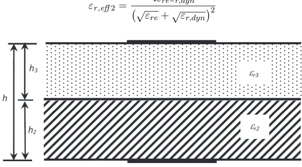
The lower patch is treated as a ground plane of upper patch [26], and the upper patch is analyzed as a rectangular patch on two dielectric layers as shown in Fig. 4. The effective permittivity of this two-layer structure (Fig. 2) is obtained as [34]:
εr,eff2 =
4εreεr,dyn
√
εre+√εr,dyn2 (24)
here, εre is the equivalent relative permittivity of the medium below the patch, and εr,dyn is dynamic permittivity. The term εr,eff2 is introduced to take into account the effect of εre, the equivalent permittivity of the medium below the patch in combination with the dynamic permittivity εr,dyn to improve the model. The computational details ofεreand εr,dyn are presented in Appendix B. The sizes of the lower and upper patches may be same or different.
2.2.2. Effective Patch Length
The effective patch length for this cavity is obtained as
b2eff =b2(1 +qb2)1/2 (25)
The derivation ofqb2 is presented in Eq. (B13) of Appendix B.
2.2.3. Resonant Frequency
The dominant mode resonant frequency for the upper patch is defined as [33]:
fr2 =
c
2b2eff√εr,eff2
(26)
withεr,eff2 and b2eff given by Eqs. (24) and (25), respectively.
2.2.4. Quality Factor
The field radiated from the lower patch depends on the lower substrate. A thicker lower substrate will increase the radiated power from the lower patch. A lower patch stops resonating for lower substrate thickness greater than 0.11λ0 (εr1 = 2.5). The dielectric constant of lower substrate plays a role similar to that of its thickness. A low value ofεr1 for the substrate will increase the fringing field at the patch periphery, and thus the radiated power [3]. The fields that radiate from the lower patch are coupled with the upper patch [26]. So, the lower substrate will affect the upper cavity.
QT2 is defined as [26]:
QT2 =
h h1
1
Qr2
+ 1
Qd2
+ 1
Qc2 −1
(27)
hereh/h1 represents the coupling factor.
Qr2 is defined in [30] as
Qr2 =
c√εr,eff2 4hfr2
(28)
whereεr,eff2 is defined in Eq. (24), and fr2 is obtained from Eq. (26).
Qd2 and Qc2 can be computed as [35]:
Qd2 =
π√εr,eff2
λr2αd
(29)
Qc2 =
π√εr,eff2
λr2(αc+αf eed)
(30)
hereαd is the dielectric loss, andαc is the conductor loss. The computational details ofαdand αc are available in [36]:
αd =
εre
εre−1
εr,eff2−1
√ε
r,eff2
tanδe2
λr2
(31)
tanδe2 =
εr2h2tanδ2+εr3h3tanδ3
hεre (32)
αc =
RS
Zrα2
Zr = √120π
εr,eff2
α
2
h + 1.393 + 0.667 ln
α
2
h + 1.444
−1
(34)
RS = πfr2μ0/σ (35)
αf eed is the loss due to the feed, and it can be neglected. εr,eff2, εre and fr2 are given by Eqs. (24), (B1) and (26), respectively.
2.2.5. Efficiency, Directivity and Gain
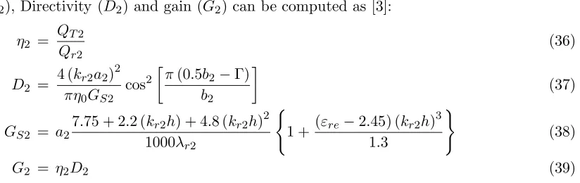
The efficiency (η2), Directivity (D2) and gain (G2) can be computed as [3]:
η2 =
QT2
Qr2
(36)
D2 =
4 (kr2a2)2
πη0GS2 cos2
π(0.5b2−Γ)
b2
(37)
GS2 = a2
7.75 + 2.2 (kr2h) + 4.8 (kr2h)2 1000λr2
1 +(εre−2.45) (kr2h) 3
1.3
(38)
G2 = η2D2 (39)
2.2.6. Input Impedance
Like the lower patch, the upper patch is also treated as a resonant cavity modeled by a single resonant parallelL2,C2 and R2 circuit as shown in Fig. 5. The input impedance of upper cavity is defined as
Zin2 =
Rin2
1 +Q2T2A2 +j
Rin2QT2A 1 +Q2T2A2
(40)
here,
Rin2 = Rr2cos2
π(0.5b2−Γ)
b2
(41)
A =
fr2
f − f fr2
(42)
Rr2 is obtained from [37] as
Rr2 =
2η0QT2h
π√εr,eff2a2eff
(43)
a2eff = a2(1 +qa2)1/2 (44)
withεr,eff2 defined in Eq. (24),qa2 obtained from Eq. (B14), andQT2 given by Eq. (27).
3. ANTENNA DESIGN AND EXPERIMENTAL TESTS
The prototypes are etched on a Taconic substrate having a1 = a2 = 30.0 mm, b1 = b2 = 30.0 mm,
h1 = h3 = 0.7875 mm, εr1 = εr3 = 2.33, tanδ1 = tanδ3 = 0.001. The lower patch is excited with a coaxial probe of diameter d = 1.24 mm located at a distance ρ = 8.0 mm as shown in Fig. 1. To validate the models developed in Section 2, we perform some of the experiments using Network Analyzer Agilent E5071B. The measured resonance is defined as the maximum resistance point. We have previously mentioned in Sections 2.1 and 2.2 that the lower patch is analyzed as a patch covered with multi-dielectric layers, and upper patch is analyzed as a patch without dielectric cover. The effective permittivity of microstrip structure is enhanced, and thus the fringing field effect is decreased for a patch covered with multi-dielectric layers compared to the patch without dielectric cover [28, 29]. Thus, the resonant frequency for a dielectric covered patch antenna is lowered compared to the patch without dielectric cover. So, the lower resonance is treated for lower patch, and upper resonance is considered for upper patch.
4. RESULTS AND DISCUSSIONS
In this section, we present the theoretically predicted, simulated and measured results for the resonant frequency, quality factors, bandwidth, efficiency, directivity, gain and input impedances for this structure.
4.1. Three Layers Structure with Both Driven and Parasitic Patches
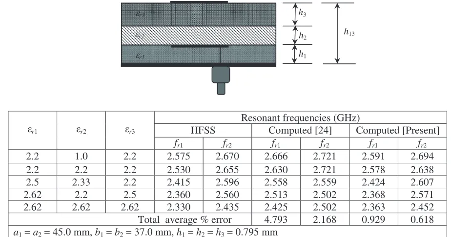
In Table 1, we compare the computed resonant frequencies employing the present model with the results of model reported in [24] and HFSS [25] simulation results for different sets of relative permittivities of the layered substrate. The thicknesses of the layers are assumed as h1 =h2 =h3 = 0.795 mm, and the dimensions of both patches are considered to bea1 =a2 = 45.0 mm andb1 =b2 = 37.0 mm. The errors in results against the HFSS simulation results of the present model are much less than the errors in results of the model reported in [24].
Table 1. Comparison of theoretically predicted resonant frequencies and HFSS simulated resonant frequencies for a three-layer stacked rectangular patch antenna with different sets of relative permittivities of the layered substrate.
εr1 εr2 εr3
Resonant frequencies (GHz)
HFSS Computed [24] Computed [Present]
fr1 fr2 fr1 fr2 fr1 fr2
2.2 1.0 2.2 2.575 2.670 2.666 2.721 2.591 2.694
2.2 2.2 2.2 2.530 2.655 2.630 2.721 2.578 2.638
2.5 2.33 2.2 2.415 2.596 2.558 2.559 2.424 2.607
2.62 2.2 2.5 2.360 2.560 2.513 2.502 2.368 2.571
2.62 2.62 2.62 2.330 2.435 2.425 2.502 2.363 2.452
Total average % error 4.793 2.168 0.929 0.618
a1 = a2 = 45.0 mm, b1 = b2 = 37.0 mm, h1 = h2 = h3 = 0.795 mm
h1
h2
h3
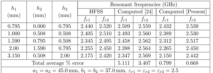
The computed resonant frequencies employing the present model and the model reported in [24] along with corresponding HFSS resonant frequencies of two patches versus the thickness of the layers are presented in Table 2. The permittivities of the layers are assumed asεr1 =εr2 =εr3= 2.5, and the dimensions of both patches are considered to bea1 =a2= 45.0 mm andb1 =b2 = 37.0 mm. The errors in results of present model and model in [24] are calculated against HFSS simulation results. The total average error indicates that the present model more accurately computes the resonant frequencies.
Table 2. Comparison of theoretically predicted resonant frequencies and HFSS simulated resonant frequencies for a three-layer stacked rectangular patch antenna with different sets of thickness of the layered substrate.
h1 (mm)
h2 (mm)
h3 (mm)
Resonant frequencies (GHz)
HFSS Computed [24] Computed [Present]
fr1 fr2 fr1 fr2 fr1 fr2
0.795 0.000 0.795 2.440 2.520 2.509 2.559 2.432 2.539
1.000 0.508 0.508 2.405 2.510 2.493 2.560 2.389 2.530
1.590 0.795 0.508 2.345 2.495 2.458 2.562 2.312 2.517
2.00 1.590 0.795 2.255 2.450 2.398 2.564 2.265 2.450
3.150 0.508 2.00 2.175 2.420 2.347 2.569 2.150 2.442
Total average % error 5.111 3.407 0.799 0.668
a1 =a2= 45.0 mm, b1=b2= 37.0 mm, εr1 =εr2 =εr3= 2.5
The required frequency separation (fr2 −fr1) can be obtained by adjusting the parameters and thickness of the layers. Once fr2 and fr1 are determined, the bandwidth can be enlarged considering the center frequency as the matching frequency given byfr= 0.5×(fr1+fr2). The required frequency separation can also be obtained by adjusting the dimensions of the patches. There is a mutual coupling between the two resonances. The mutual coupling between two resonances is not adjusted by the change of dimensions of the patches, but the substrate thickness and permittivity variation between two resonators adjust the mutual coupling between them resulting in wide bandwidth [3]. Thus, we consider the variation of dielectric structure instead of variation of dimensions of patches.
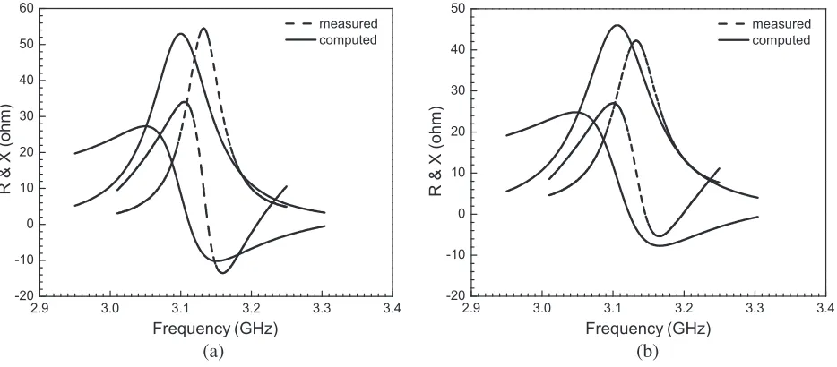
The computed resistance (R) and reactance (X) curves employing the present model are compared with HFSS simulated curves in Fig. 6, and very good agreements are observed between them. The parameters for this study are considered as a1 = a2 = 45.0 mm, b1 = b2 = 37.0 mm, h1 = 1.0 mm,
h2 =h3= 0.508 mm, εr1=εr2 =εr3 = 2.5, tanδ1= tanδ2 = tanδ3 = 0.0025 andρ= Γ = 15.00 mm. In Fig. 7 we compare the computed R and X curves employing the present model with our experimental curves for two different air dielectric spacings (h2 = 5.0 mm and 8.0 mm) in between lower patch and the substrate of upper patch. The parameters for this study are taken asa1 =a2= 30.0 mm,
b1 = b2 = 30.0 mm, h1 = h3 = 0.7875 mm, εr1 = εr3 = 2.33, εr2 = 1.0, tanδ1 = tanδ3 = 0.001, tanδ2= 0.000 andρ= Γ = 8.00 mm.
The comparison between our measuredRandXcurves and computed curves employing the present model for two different PTFE dielectric spacings (h2 = 0.508 with εr2 = 2.2 mm and 0.7875 mm with 2.33) in between lower patch and the substrate of upper patch in Fig. 8. The parameters for this study are considered as a1 = a2 = 30.0 mm, b1 = b2 = 30.0 mm, h1 = h3 = 0.7875 mm, εr1 = εr3 = 2.33, tanδ1 = tanδ3= 0.001 and ρ= Γ = 8.00 mm. The second resonance is disappearing in this case [24].
2.25 2.30 2.35 2.40 2.45 2.50 2.55 2.60 2.65 -100
-50 0 50 100 150
Upper Cavity computed
HFSS
Lower Cavity
Frequency (GHz)
R
&
X
(ohm)
Figure 6. Computed and HFSS simulated input impedances for a three-layer stack patch. a1 =
a2 = 45.0 mm, b1 = b2 = 37.0 mm, h1 = 1.0 mm, h2 = h3 = 0.508 mm, εr1 = εr2 = εr3 = 2.5, tanδ1= tanδ2 = tanδ3= 0.0025, ρ= Γ = 15.00 mm.
2.9 3.0 3.1 3.2 3.3 3.4
-20 -10 0 10 20 30 40 50 60
measured computed
2.9 3.0 3.1 3.2 3.3 3.4
-20 -10 0 10 20 30 40 50
measured computed
(a) (b)
Frequency (GHz)
R
&
X
(ohm)
Frequency (GHz)
R
&
X
(ohm)
Figure 7. Computed and measured input impedances for a three-layer stack patch. a1 =a2= 30.0 mm,
b1 = b2 = 30.0 mm, h1 = h3 = 0.7875 mm, εr1 = εr3 = 2.33, εr2 = 1.0, tanδ1 = tanδ3 = 0.001, tanδ2= 0.000, ρ= Γ = 8.00 mm. (a)h2 = 5.0 mm, (b) h2 = 8.0 mm.
structures in Sections 4.1 and 4.2. Sections 4.3 and 4.4 are introduced to validate the model developed for a patch covered with dielectric layers and the patch without dielectric layer, respectively. At the end of Section 4.1, we use the same superstrate permittivity as that in Section 4.2 in order to observe the change of lower and upper resonances for the three-layer structure compared to the two-layer structure.
4.2. Two Layers Structure with Both Driven and Parasitic Patches
2.8 2.9 3.0 3.1 3.2 3.3 -40
-30 -20 -10 0 10 20 30 40 50 60 70
computed measured
2.8 2.9 3.0 3.1 3.2 3.3
-40 -30 -20 -10 0 10 20 30 40 50 60 70
computed measured
(a) (b)
Frequency (GHz)
R
&
X
(ohm)
Frequency (GHz)
R
&
X
(ohm)
Figure 8. Computed and measured input impedances for a three-layer stack patch. a1 =a2= 30.0 mm,
b1 =b2 = 30.0 mm, h1 =h3 = 0.7875 mm, εr1 =εr3 = 2.33, tanδ1 = tanδ3 = 0.001, ρ= Γ = 8.00 mm. (a)h2= 0.508 mm, εr2= 2.2, tanδ2 = 0.0009, (b)h2 = 0.7875 mm,εr2 = 2.33, tanδ2 = 0.001.
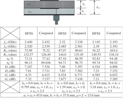
Table 3. Comparison of theoretically predicted and HFSS simulated resonant frequencies, input impedances, efficiencies, directivities and gains for a two-layer stacked rectangular patch antenna with different layered thicknesses.
HFSS Computed HFSS Computed HFSS Computed
fr1 (GHz) 2.440 2.432 2.32 2.338 .145 .193
fr2 (GHz) 2.520 2.539 2.485 2.501 2.39 2.393
Rr1 (ohm) 72.99 75.22 87.07 90.63 1.22 104.4
Rr2(ohm) 132.57 126.49 144.0 135.45 149.55 138.14
η1 % 73.21 77.43 87.10 88.59 2.82 4.48
η2 % 90.13 89.656 94.71 96.75 9.74 8.92
D1 (dB) 7.247 7.526 7.06 7.297 6.524 6.898
D2 (dB) 7.81 7.711 7.83 7.582 7.23 7.252
G1 (dB) 6.33 6.415 6.524 6.771 6.585 6.652
G2 (dB) 7.32 7.237 7.677 7.438 7.21 7.205
h2 = 0.0 mm, h1 = h3 =
0.795 mm, εr2 = 1.0, εr1
= εr3 = 2.5
h2 = 0.0 mm, h1 = h3
= 1.59 mm, εr2 = 1.0,
εr1 = εr3 = 2.5
h2 = 0.0 mm, h1 = h3 =
3.18 mm, εr2 = 1.0, εr1
= εr3 = 2.5
a1 = a2 = 45.0 mm, b1 = b2 = 37.0 mm, ρ = = 15.0 mm
r1 h1
h3
r3
h13
Γ ε
ε
2 2
9
9 9
2.9 3.0 3.1 3.2 3.3 3.4 0
10 20 30 40 50 60 70 80 90
Upper Cavity computed
HFSS
Lower Cavity
Frequency (GHz)
R
(ohm)
in
Figure 9. Computed and HFSS simulated input resistances for a two-layer stack patch. a1 = a2 = 30.0 mm, b1 = b2 = 30.0 mm, h1 = h3 = 0.7875 mm, h2 = 0.0 mm, εr1 = εr3 = 2.33, εr2 = 1.0, tanδ1= tanδ3 = 0.001, tanδ2 = 0.000,ρ= Γ = 7.00 mm.
2.2 2.3 2.4 2.5 2.6
-150 -100 -50 0 50 100 150 200
Upper Cavity computed
HFSS measured [21]
Lower Cavity
Frequency (GHz)
R
&
X
(ohm)
Figure 10. Computed, measured and HFSS simulated input impedances for a two-layer stack patch.
a1 =a2 = 45.0 mm, b1 =b2 = 37.0 mm, h2 = 0.0 mm, h1 =h3 = 1.59 mm, εr1 =εr3 = 2.5, εr2 = 1.0, tanδ1= tanδ3 = 0.0025, tanδ2 = 0.000,ρ= Γ = 15.00 mm.
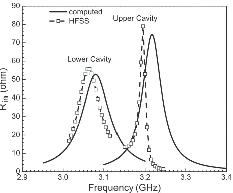
In Fig. 9, the computed input resistance curves are compared with the HFSS simulated curves, and close agreement is seen between them. For this study, we consider the parameters asa1 =a2= 30.0 mm,
b1 = b2 = 30.0 mm, h1 = h3 = 0.7875 mm, h2 = 0.0 mm, εr1 = εr3 = 2.33, εr2 = 1.0, tanδ1 = tanδ3= 0.001, tanδ2 = 0.000 and ρ= Γ = 7.00 mm.
The computed, measured [21] and HFSS simulated input resistance and reactance curves are depicted in Fig. 10. The computed curves agree very well with the HFSS simulated ones. The parameters are taken for this study as a1 =a2 = 45.0 mm, b1 =b2 = 37.0 mm, h2 = 0.0 mm, h1 =h3 = 1.59 mm,
εr1=εr3 = 2.5,εr2 = 1.0, tanδ1= tanδ3 = 0.0025, tanδ2= 0.000 and ρ= Γ = 15.00 mm.
0 2 4 6 8 10 12 14 16 0
20 40 60 80 100 120 140 160 180 200 220
Lower Cavity computed
HFSS Upper Cavity
Feed location (mm)
R
(ohm)
in
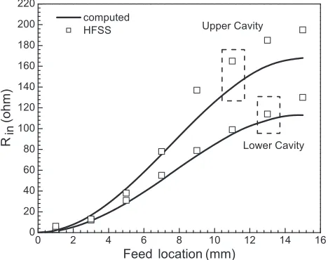
Figure 11. Theoretical and HFSS simulation input resistances at resonances as a function of feed location. a1 =a2 = 30.0 mm,b1 =b2 = 30.0 mm, h1 =h3= 0.7875 mm, h2 = 0.0 mm,εr1 =εr3= 2.33,
εr2= 1.0, tanδ1 = tanδ3= 0.001, tanδ2= 0.000.
The discrepancy is observed between the computed and simulated values for the upper cavity. This is because we have assumed that the field radiated by the lower patch is coupled with the upper patch, and a virtual feed location Γ exists. Γ is not an actual feed location point but held as a virtual feed location point.
The discrepancy is observed among the measured, HFSS and theoretical curves in Figs. 7–11. This is due to the following facts: (i) In experimental procedure, a little air gap may be present with the PTFE dielectric spacing or in between lower patch and the substrate of upper patch which cannot be avoided. So, the effective permittivity is changed, and thus the resonant frequency and input impedances are also changed. This fact will introduce errors in the model. (ii) We previously stated that the lower patch behaved as a ground plane of upper patch. So, the lower patch does not provide a large ground plane, and this fact also introduces errors in the model [9]. (iii) The fields radiated by the lower patch are electromagnetically coupled with the upper patch. Some of the fields of lower patch are shared with air, and the rest is electromagnetically coupled with the upper patch. This fact also introduces errors in the model. (iv) The virtual feed location for upper patch also produces error in the model.
4.3. Parasitic Patch with and without Air-Gap and Driven Patch is Absent
In Table 4, we compare the dominant mode resonant frequencies employing the present model and models reported in [38, 39] with the experimental results from [40] for a rectangular patch on a single layer. The total average error shows that the present model more accurately computes the resonant frequencies. In Section 2.1, we have already mentioned that the lower patch behaves as a ground plane of the upper patch. Thus, the lower patch does not behave as the large ground plane for the upper patch. However, here we consider the large ground plane (Appendix B, Fig. B1) for developing the model. So, there is a little discrepancy between the measured and computed values employing the present model.
The computed input resistance and reactance curves employing the present model are compared with our measured curves in Fig. 12, and very good agreement is revealed between them. The parameters for this study are a2 = 30.0 mm, b2 = 20.0 mm, h1 =h2 = 0.0 mm, h3 = 0.7875 mm,εr1 =εr2 = 1.0,
εr3= 2.32, tanδ3= 0.001 and Γ = 6.00 mm.
Table 4. Comparison of experimental dominant mode resonant frequencies from [40] with theoretically predicted values obtained from closed form models presented in [38, 39] and in this work for a rectangular patch.
a2
(mm)
b2
(mm)
h3
(mm)
Resonant Frequency (GHz)
Exp.
[40] [38] [39] Model
57.0 38.0 3.175 2.31 2.38 2.30 2.38
45.5 30.5 3.175 2.89 2.90 2.79 2.90
29.5 19.5 3.175 4.24 4.34 4.11 4.27
19.5 13.0 3.175 5.84 6.12 5.70 5.90
17.0 11.0 3.175 6.80 7.01 6.47 6.70
14.0 9.0 3.175 7.70 8.19 7.46 7.74
12.0 8.0 3.175 8.27 9.01 8.13 8.40
10.5 7.0 3.175 9.14 9.97 8.89 9.18
9.0 6.0 3.175 10.25 11.18 9.82 10.13
Total Average % Error 5.23 2.88 1.14
Average % Error = [(exp. – theory)/ exp.]×100
r3 =2.33, r1 = εr2 =1.0, h1 = h2 = 0.0 mm
h3
r3
ε ε
ε
4.5 4.6 4.7 4.8 4.9 5.0
-40 -20 0 20 40 60 80
Computed Exp.
Frequency (GHz)
R
(ohm)
in
Figure 12. Computed and measured input impedances for a rectangular patch on single substrate.
a2 = 30.0 mm, b2 = 20.0 mm, h1 = h2 = 0.0 mm, h3 = 0.7875 mm, εr1 = εr2 = 1.0, εr3 = 2.32, tanδ3= 0.001, Γ = 6.00 mm.
4.4. Driven Patch with Flush and Spaced Dielectric Superstrates and Parasitic Patch Is Absent
0.0 0.2 0.4 0.6 0.8 1.0 4.4
4.6 4.8 5.0 5.2 5.4 5.6
8.0 8.5 9.0 9.5 10.0
Computed Exp. HFSS
h (mm)
Gain
(dB)
Frequency
(GHz)
2
Figure 13. Computed, measured and HFSS simulated resonant frequencies and gains for a rectangular patch on the suspended substrate. a2 = 30.0 mm, b2 = 20.0 mm, h1 = 0.0 mm, h2 is variable,
h3 = 0.7875 mm,εr1=εr2 = 1.0,εr3= 2.32.
Table 5. Comparison of theoretically predicted and measured resonant frequencies for a rectangular patch with spaced dielectric superstrate for wide range of permittivity (εr3) variation.
r3 h3
(mm)
Resonant Frequency (GHz)
Exp. Model
2.20 0.508 3.71 3.715
2.32 1.575 3.71 3.717
2.55 2.385 3.72 3.718
2.40 1.580 3.71 3.716
5.00 1.630 3.70 3.695
5.60 1.400 3.69 3.690
9.80 1.630 3.65 3.679
Total Average % Error
0.209
a1 = 30.0 mm, b1 = 23.0 mm, h1=
1.58 mm, h2 = 5.0 mm, r1 = 2.4,
r2 = 1.0
h1
h3
h13
h2
ε
ε ε
Table 6. Comparison of theoretically predicted and measured resonant frequencies for a rectangular patch with flush dielectric superstrate for wide range of permittivity (εr3) variation.
r3 (mm) h3
Resonant Frequency (GHz)
Exp. HFSS [41] Model
2.2 0.508 3.05 3.03 3.09 2.93
2.32 1.575 3.01 2.97 3.09 2.92
2.55 2.385 2.99 2.94 3.08 2.90
5.0 1.630 2.92 2.82 3.07 2.87
5.6 1.400 2.94 2.81 3.08 2.86
9.8 1.630 2.74 2.67 3.07 2.78
a1 = 30.0 mm, b1 = 30.0 mm, h1 = 1.58 mm, h2= 0.0
mm, r1 = 2.4
Total average error (%) 4.82*
7.37**
2.64* 2.32** * error against exp. and ** error against HFSS
h1
h3
h13
ε
ε
Figure 14 depicts the comparison of computed input resistance and reactance curves with our experimental curves for a rectangular patch with flush superstrate. The close correlation is seen between them.
3.75 4.00 4.25 4.50 4.75 5.00 5.25 -40
-20 0 20 40 60 80
Exp. Computed
Frequency (GHz)
R
&
X
(ohm)
Figure 14. Computed and measured input impedances for a rectangular patch with flush superstrate.
5. CONCLUSION
In this article, a simple design guideline is proposed to investigate the resonant frequency, quality factor, bandwidth, efficiency, directivity, gain and input impedance of a stack rectangular patch antenna. The advantages of this model are the mathematical simplicity and low computation cost, and it is faster than the numerical methods and commercially available software. This model is directly applicable to the CAD programs. The computed values are compared with the experimental results available in open literature and our experimental results. We also employ electromagnetic software (HFSS) to generate some results. The present model shows much less error than the experimental and HFSS simulation results. The superiority of the model is that it is also very valid for a rectangular patch on a multilayered substrate and a rectangular patch with flush and spaced dielectric. This model is very useful for practical implementation of a patch on a multilayered substrate, patch with flush and spaced dielectric superstrate and stack rectangular patch antenna in broad band application.
APPENDIX A. DETERMINATION OF EFFECTIVE PERMITTIVITY (εr,eff1), AND
RELATIVE PERMITTIVITY (εrr) OF LOWER CAVITY
The three-layer structure shown in Fig. A1(a) is conformally mapped onto a complexgplane (g=u+jv) with results as shown in Fig. A1(b) based on the method reported in [42] for generalized multilayered microstrip. The filling fraction pi is defined as the ratio of each dielectric area Si (i = 1,2,3) to the entire area of the cross section SC in the g plane [43, 44]. The filling fractions pi =Si/SC for each of these three layers for the wide strip structure (a1/h1 ≥1) are defined as [42]
p1 =
S1
SC = 1−
ln
πa1eff
h1 − 1
2a1eff
h1
(A1)
(b)
(c)
Figure A1. (a) Top view and cross-sectional view of the rectangular patch antenna structure under study. (b) Conformally mapped equivalent parallel plate structure with region of note enclosed by the dashed line. (c) Approximate distribution of dielectric materials between parallel plates as presented in [41] and [42].
p2 =
S2
SC = 1−p1− h1−v
2a1eff ln
⎡ ⎢ ⎢ ⎣πa1eff
h1
cos(πv/2h1)
π
h13
h1
−1
2 +
v
2
π h1
+ sin(πv/2h1) ⎤ ⎥ ⎥
p3 =
S3
SC =
h1−v 2a1eff
ln ⎡ ⎢ ⎢ ⎣πa1eff
h1
cos(πv/2h1)
π
h13
h1 − 1 2 + v 2 π h1
+ sin(πv/2h1) ⎤ ⎥ ⎥
⎦ (A3)
v = 2h1
π arctan
⎡ ⎢
⎣π π
2
a1eff
h1 − 2
h13
h1 − 1
⎤ ⎥
⎦ (A4)
The filling fraction expressions developed by [41] and [42] ignore the behavior in the limit when there is no superstrate. In this case, h13 =h1,v in Equation (A4) goes to zero, andp2 should also go to zero. However,p2 as given in Eq. (A2), does not go to zero in this limit, indicating that the model developed in both [41] and [42] overestimates the filling fraction of the superstrate in all situations. To rectify this inconsistency, a new filling fractionp3 equal to half the value ofp2 in the limit whenh13=h1 was reported in [28]:
p4=
h1 2a1eff
ln
π
2 −
h1 2a1eff
(A5)
This new filling fraction is used to modify two of the existing filling fractions, withp1nandp2nnow given by
p1n = p1−p4 (A6)
p2n = 1−p1n−p3−2p4 (A7) withp3given by Eq. (A3). The terma1eff present in Eqs. (1A)–(5A) is defined as an effective line width of the lower patch and computed as
a1eff =
εrr/εr,eff1
a1+ 0.882h1+ 0.164h1
(εrr−1) (εrr)2
+h1
(εrr−1)
πεrr {ln(0.94 +a1/2h1) + 1.451}
(A8)
here,εrris the relative permittivity of an ideal single substrate microstrip structure under consideration, andεr,eff1is the composite effective permittivity of the multilayer structure. In order to compute a1eff, a two-step iteration is considered starting with an approximationεrr =εr1andεr,eff1 =εrr. Onceεr,eff1 andεrr are determined using this first value ofa1eff, Eq. (A8) is employed to compute the effective line width a second time.
The distribution and propagation of the electric field lines within the structure under test can be best explained by [28]. As shown in Fig. A2, the electric field flux lines are capable of following three different paths in the structure under study. Path 1 reflects the flux within the substrate of the structure. Path 2 represents the flux that exists strictly in the superstrate and the substrate. Finally, the flux line is extended into the material above the superstrate by path 3. The derivation of effective permittivity, εeff1, of the parallel plate structure visualized in Fig. A3 yields [28]:
εr,eff1 = εr1p1n+εr1(1−p1n) 2
(A9)
×
ε2
r2p2np3+εr2εr3
p2np4+ (p3+p4)
2
ε2r2p2np3p4+εr1(εr2p3+εr3p4) (1−p1n−p4)2 +εr2εr3p4
p2np4+{p3+p4}2
(A10)
The computation of effective permittivity of the structure in Fig. A1(a) employing Eq. (9A) allows consideration of the structure as an equivalent microstrip structure with semi-infinite superstrate with relative permittivity equal to unity and a single dielectric substrate with relative permittivity equal to
εrr=
2εr,eff1−1 +
1 + 10h1
a1eff
−1/2
1 +
1 + 10h1
a1eff
Figure A2. Illustration of electric flux paths for the structure shown in Fig. A1(a).
Figure A3. Proposed filling fraction arrangement for calculation of effective permittivity that preserves the electric flux paths described in Fig. 2. The region to the extreme right (S1, εr1) reproduces the capacitive effect of electric flux Path 1. The region containingS2 (εr2) and a portion ofS4 with relative permittivity equal to εr1 reproduce the capacitive effect of electric flux Path 2. The remaining region to the extreme left containingS3 (εr3),S4 (εr2), and a portion ofS4 with relative permittivity equal to
εr1 reproduces the capacitive effect of electric flux Path 3.
APPENDIX B. DETERMINATION OF EFFECTIVE PERMITTIVITY (εr,eff2) OF UPPER CAVITY
Figure B1. Top view and cross-sectional view of the rectangular patch antenna structure under study.
and the two-layer structures, the two-layer structure is modeled as the single-layer one having substrate thickness of h =h3+h2 and an equivalent substrate relative permittivity ofεre determined under the cavity model approximations as
εre=
εr2εr3h
εr2h3+εr3h2
(B1)
In order to account for the influence of the fringing field at the edge of the rectangular patch, the term dynamic permittivity is considered. The dynamic permittivityεr,dyn depends on the dimensions (a2,b2,
h), equivalent substrate relative permittivity εre, and field configuration of the mode under study [45]. It can be expressed as
εr,dyn = Cdyn(ε=ε0εre)
Cdyn(ε=ε0)
(B2)
In Equation (B2), Cdyn(ε) is the total dynamic capacitance of the condenser formed by the conducting patch and the ground plane separated by a dielectric of permittivity ε. Cdyn(ε0) is the total dynamic capacitance whenε=ε0. TheCdyn(ε) can be written as
Cdyn(ε) =C0,dyn(ε) + 2Ce1,dyn(ε) + 2Ce2,dyn(ε) (B3)
whereCo,dyn is the dynamic main field capacitance without considering the fringing field. This can be calculated as
C0,dyn(ε) =
ε0εrea2b2
hδnδm =
C0,stat(ε)
δnδm (B4)
C0,stat(ε) =
ε0εrea2b2
h (B5)
where, Co,stat(ε) represents the static main field capacitance without fringing field, and δn and δm are in the form
δi = 1 for i= 0
= 2 for i= 0 (B6)
and the dynamic edge capacitance Ce2,dyn(ε) on one side of patch width a2 can be computed as
Ce1,dyn(ε) = 1
δnCe1,stat(ε) (B7)
Ce2,dyn(ε) = 1
δm
Ce2,stat(ε) (B8)
where, Ce1,stat(ε) represents the static edge capacitance on one side of patch length b2, and Ce2,stat(ε) represents the static edge capacitance on one side of patch width a2.
The static edge capacitance for a circular disk was reported in [46]. Based on this concept, the static edge capacitance for rectangular patch can be computed as
Ce= ε0εrea2b2
h (1 +qb2+qa2) (B9)
In Eq. (9B), the first term represents the static main capacitance Co,stat(ε), and qb2 and qa2 arise due to the fringing field at the edge of patch lengthb2and patch widtha2, respectively. Thus,Ce1,stat(ε) and Ce2,stat(ε) are defined as
Ce1,stat(ε) = 0.5C0,stat(ε)qb2 (B10) and
Ce2,stat(ε) = 0.5C0,stat(ε)qa2 (B11)
qb2 and qa2 are the fringing field factors at the edge of the patch length b2 and at the edge of the patch widtha2, respectively. The fringing field factorq at the edge of a circular patch of radiusrwas reported in [47] as
q= 2h
πrεre log r 2h
+ (1.41εre+ 1.77) +h
r (0.268εre+ 1.65)
(B12)
From Eq. (B12), qa2 and qb2 of the rectangular patch of width a2 and length b2 are determined. For computing qb2 and qa2, an equivalence relation between a rectangular patch and a circular patch is considered. To account for equal static fringing fields, equal circumference is considered as the basis of equivalence, resulting ina2 ≈(π−2)r andb2≈2r[30]. Thusqb2 andqa2 for this structure are obtained as
qb2 =
1.273h b2εre
log
b2
4h + (1.41εre+ 1.77) +
2h b2
(0.268εre+ 1.65)
(B13)
qa2 =
0.727h a2εre
log
a
2 2.284h
+ (1.41εre+ 1.77) +1.142h
a2
(0.268εre+ 1.65)
(B14)
Now we define the effective permittivity of upper patch as [34]:
εr,eff2 =
4εreεr,dyn
√
εre+√εr,dyn2 (B15)
REFERENCES
1. Kumar, G. and K. P. Ray, Broadband Microstrip Antennas, Artech House, London, 2003.
2. Carver, K. R. and J. W. Mink, “Microstrip antenna technology,”IEEE Trans. Antennas Propagat., Vol. 29, 2–23, Jan. 1981.
3. Garg, R., P. Bhartia, I. Bahl, and A. Ittipiboon, Microstrip Antenna Design Handbook, Artech House, Canton, MA, 2001.
4. Waterhouse, R. B.,Printed Antennas for Wireless Communications, John Wiley & Sons, England, 2007.
5. Jin, Y. and Z. Du, “Broadband dual-polarized F-probe fed stacked patch antenna for base stations,”
IEEE Antennas Wireless Propagate. Lett., Vol. 14, 1121–1124, 2015.
7. Ali, M., T. M. Sayem, and V. K. Kunda, “A reconfigurable stacked microstrip patch antenna for satellite and terrestrial links,” IEEE Trans. Vehic. Technol., Vol. 56, 426–435, Mar. 2007.
8. Zhou, Y., C.-C. Chen, and J. L. Volakis, “Dual band proximity-fed stacked patch antenna for tri-band GPS applications,” IEEE Trans. Antennas Propagat., Vol. 55, 220–223, Jan. 2007. 9. Wang, Z., S. Fang, S. Fu, and S. Lv, “Dual-band probe-fed stacked patch antenna for GNSS
applications,” IEEE Antennas Wireless Propagate. Lett., Vol. 8, 100–103, 2009.
10. Li, D., P. Guo, Q. Dai, and Y. Fu, “Broadband capacitively coupled stacked patch antenna for GNSS applications,”IEEE Antennas Wireless Propagate. Lett., Vol. 11, 701–704, 2012.
11. Falade, O. P., M. U. Rehman, Y. Gao, X. Chen, and C. G. Parini, “Single feed stacked patch circular polarized antenna for triple band GPS receivers,”IEEE Trans. Antennas Propagat., Vol. 60, 4479– 4484, Oct. 2012.
12. Wang, Z., S. Fang, S. Fu, and S. Jia, “Single-fed broadband circularly polarized stacked patch antenna with horizontally meandered strip for universal UHF RFID applications,” IEEE Trans. Micro. Theory Tech., Vol. 59, 1066–1073, Apr. 2011.
13. Gao, Y., R. Ma, Y. Wang, Q. Zhang, and C. Parini, “Stacked patch antenna with dual-polarization and low mutual coupling for massive MIMO,”IEEE Trans. Antennas Propagat., Vol. 64, 4544–4549, Oct. 2016.
14. Hu, J., Z.-C. Hao, and W. Hong, “Design of a wideband quad-polarization reconfigurable patch antenna array using a stacked structure,” IEEE Trans. Antennas Propagat., Vol. 65, 3014–3023, Jun. 2017.
15. Tiwari, H. and M. V. Kartikeyan, “A stacked microstrip patch antenna with fractal shaped defects,”
Progress In Electromagnetics Research C, Vol. 14, 185–195, 2010.
16. Ghorbani, K. and R. B. Waterhouse, “Dual polarized wide-band aperture stacked patch antennas,”
IEEE Trans. Antennas Propagat., Vol. 52, 2171–2174, Aug. 2004.
17. Anguera, J., C. Puente, and C. Borja, “A procedure to design stacked microstrip patch antennas based on a simple network model,”Micro. Opt. Technol. Lett., Vol. 30, 149–151, Aug. 2001. 18. Anguera, J., C. Puente, C. Borja, N. Delbene, and J. Soler, “Dual-frequency broad-band stacked
microstrip patch antenna,”IEEE Antennas Wireless Propagate. Lett., Vol. 2, 36–39, 2003.
19. Jang, W.-G. and J.-H. Choi, “Design of a wide and multiband aperture-stacked patch antenna with reflector,”Micro. Opt. Technol. Lett., Vol. 49, 2822–2824, Nov. 2007.
20. Lee, R. Q. and K. F. Lee, “Experimental study of the two-layer electromagnetically coupled rectangular patch antenna,”IEEE Trans. Antennas Propagat., Vol. 38, 1298–1302, Aug. 1990. 21. Hassani, H. R. and D. M. Syahkal, “Study of electromagnetically coupled stacked rectangular patch
antennas,”IEE Proc. — Micro. Antennas Propagat., Vol. 142, 7–13, Feb. 1995.
22. Waterhouse, R. B., “Design of probe-fed stacked patches,” IEEE Trans. Antennas Propagat., Vol. 47, 1780–1784, Dec. 1999.
23. Reineix, A. and B. Jecko, “Analysis of microstrip patch antennas using finite difference time domain method,”IEEE Trans. Antennas Propagat., Vol. 31, 381–390, Mar. 1991.
24. Liu, Z.-F., P.-S. Kooi, L.-W. Li, M.-S. Leong, and T.-S. Yeo, “A method for designing broad-band microstrip antennas in multilayered planar structure,”IEEE Trans. Antennas Propagat., Vol. 47, 1416 –1420, Sep. 1999.
25. HFSS 13: Ansoft’s Corp.
26. Tagle, J. G. and C. G. Christodoulou, “Extended cavity model analysis of stacked microstrip ring antennas,”IEEE Trans. Antennas Propagat., Vol. 45, 1626–1635, Nov. 1997.
27. Alexopoulos, N. G. and D. R. Jackson, “Fundamental superstrate (cover) effects on printed circuit antennas,”IEEE Trans. Antennas Propagat., Vol. 32, 807–816, Aug. 1984.
28. Bernhard, J. T. and C. J. Tousignant, “Resonant frequencies of rectangular microstrip antennas with flush and spaced dielectric superstrates,”IEEE Trans. Antennas Propagat., Vol. 47, 302–308, Feb. 1999.
Lett., Vol. 56, 883–893, Apr. 2014.
30. James, J. R. and P. S. Hall, Handbook of Mcrostrip Antennas, Peter Peregrinus, London, U.K., 1989.
31. Biswas, M. and A. Mandal, “Experimental and theoretical investigation to predict the effect of superstrate on the impedance, bandwidth, and gain characteristics for a rectangular patch antenna,”
Journal of Electromagnetic Waves and Applications, Vol. 29, No. 16, 2093–2109, 2015.
32. Deshpande, M. and M. Bailey, “Input impedance of microstrip antennas,” IEEE Trans. Antennas Propagat., Vol. 30, 645–650, Jul. 1982.
33. Abboud, F., J. P. Damiano, and A. Papiernik, “Simple model for the input impedance of coax-fed rectangular microstrip patch antenna for CAD,” IEE Proc., Vol. 135, Pt. H, 323–326, Oct. 1988. 34. Chattopadhyay, S., M. Biswas, J. Y. Siddiqui, and D. Guha, “Rectangular microstrips with variable
air gap and varying aspect ratio: Improved formulations and experiments,” Micro. Opt. Technol. Lett., Vol. 51, No. 1, 169–173, Jan. 2009.
35. Verma, A. K. and Nasimuddin, “Resonance frequency and bandwidth of rectangular microstrip antenna on thick substrate,” IEEE Micro. Wireless Comp. lett., Vol. 12, 60–62, Feb. 2002.
36. Pozar, D. M., Microwave Engineering, John Wiley & Sons, Inc., Hoboken, New Jersey, 2012. 37. Khellaf, A., D. Thouroude, and J. P. Daniel, “Simple expression of rectangular patch’s resistance
at resonance,”Electron. Lett., Vol. 26, 1188–1190, Jul. 1990.
38. Hammerstad, E. O., “Equations for microstrip circuit design,” Proc. 5th European Micro. Conf., 268–272, Hamburg, Sep. 1975.
39. James, J. R., P. S. Hall, and C. Wood,Microstrip Antenna — Theory and Design, Peter Peregrinus, London, U.K., 1981.
40. Chang, E., S. A. Long, and W. F. Richards, “Experimental investigation of electrically thick rectangular microstrip antennas,”IEEE Trans. Antennas Propagat., Vol. 34, 767–772, Jun. 1986. 41. Zhong, S.-S., G. Liu, and G. Qasim, “Closed form expressions for resonant frequency of rectangular
patch antennas with multi dielectric layers,”IEEE Trans. Antennas Propagat., Vol. 42, 1360–1363, Sept. 1994.
42. Svaˇcina, J., “Analysis of multilayer microstrip lines by a conformal mapping method,”IEEE Trans. Microwave Theory Tech., Vol. 40, 769–772, Apr. 1992.
43. Wheeler, H., “Transmission-line properties of parallel wide strips by a conformal mapping approximation,” IEEE Trans. Microw. Theory Tech., Vol. 12, 280–289, Mar. 1964.
44. Wheeler, H. A., “Transmission-line properties of parallel strips separated by a dielectric sheet,”
IEEE Trans. Microwave Theory Tech., Vol. 13, 172–185, Mar. 1965.
45. Wolff, I. and N. Knoppik, “Rectangular and circular microstrip disk capacitors and resonators,”
IEEE Trans. Micro. Theory Tech., Vol. 22, 857–864, Oct. 1974.
46. Wheeler, H. A., “A simple formula for the capacitance of a disc on dielectric on a plane,” IEEE Trans. Micro. Theory Tech., Vol. 30, 2050–2054, Nov. 1982.