Available online: http://edupediapublications.org/journals/index.php/IJR/ P a g e | 924
DC-Link Capacitor Current Ripple Reduction in
DPWM based Back-to-back Converters
Mukkamalla S wathi1, R.Dileep Kumar2, Dr.A.Mallikarjuna Prasad3 1
P.G. Scholar, 2Guide, Assistant Professor, 3Head of the Department
1,2,3
Branch:-EEE(P&ID)
1,2,3
Geethanjali College of Engineering
Email id:[email protected], [email protected]
ABS TRACT
This paper proposes an improved offset selection method for discontinuous pulse-width modulation (DPWM )- based back-to-back converters to reduce DC-Link current ripple. DPWM is introduced to power converters to diminish the stress on power transistors and prolong their lifespan. However, when using the DPWM method, the DC-Link current ripple is increased in non-switching regions of the power transistors. M oreover, in DPWM -based back-to-back converters, the DC-Link current ripple reaches its maximum when the two transistors of both inverters are clamped in opposite directions. Therefore, the DC-Link capacitors endure more stress, resulting in decreased life-duration. To overcome this issue, the switching method should consider the clamping periods, when the current ripple increases. This can be achieved by modifying the DPWM offset, so that the clamping states of both converters are matched. The effectiveness of the proposed method is confirmed by both simulation and experimental results.
Keywords: Power conversion,
Capacitors, S witches, Rails, Power transistors, Transistors
INTRODUCTION
Voltage source converters (VSCs) are widely used in power generation and conversion systems and proved to be a reliable, low-cost and a highly efficient solution with many advantages such as
power factor control and improved harmonic distortion levels [1]. VSC can be controlled to operate either in a rectifier mode or in an inverter mode. With these advantages, the VSC can be found in many applications such as motor drive systems, uninterruptible power supplies (UPS), frequency converters or wind turbine generation systems [2]–[5]. It is also possible to connect several VSCs in parallel to increase the overall power rating [6] and reliability [7]. Connecting two VSCs in series yields a so-called back-to-back converter topology, when one of the VSCs is operated as a rectifier and the other one as an inverter. This topology is very
Fig. 1. Circuit configuration of a back-to-back converter.
Available online: http://edupediapublications.org/journals/index.php/IJR/ P a g e | 925
large value is always chosen for the capacitor, which increases the size of the whole system. M any researches have
attempted to find new methods to minimize the DC-Link capacitor size by reducing the current ripple. So far, the most commonly used DC-Link capacitor current ripple reduction technique is a phase-shift of two PWM carriers by 0º or 90º, depending on modulation methods. This method reduces the DC-Link current ripple value up to 50%. However, it can be applied only to a parallel connected VSC system [11]–[15].
Discontinuous pulse-width modulation (DPWM ) is used in power conversion systems to improve the efficiency with no change in the hardware or the topology. The DPWM minimizes the switching loss of the power transistors by up to 30%, and provides better harmonic characteristics at high modulation indexes (M I) [16]–[18]. For these reasons, the DPWM is used in active power filters, traction inverters, and UPS (Uninterruptible power supply) [19]– [20]. When the DPWM is used, each power transistor is being fully turned off or turned on for a certain period, usually 60 electrical degrees. The linked reference voltage is clamped to either the positive or negative DC-Link rail. At these moments, the output signal of the clamped phase is being modulated by switching the other 2 phases over the course of the period [5].
Although reducing the switching loss improves the efficiency, the DPWM method, applied to a back-to-back conversion system increases the DC-Link current ripple, and therefore causes more stress on the DC-Link capacitor. M oreover, when both converters are clamped to opposite DC-Link rails, prominent
current peaks appear in the DC-Link. As a result, the lifespan of the DC-Link component and the whole system is shortened. On the contrary, when both
VSCs are clamped to the same DC-Link rail, the current ripple is reduced. This paper proposes an improved
DPWM offset selection method to reduce the DC-Link current ripple in back-to-back converters. The reduction method is accomplished by matching the clamping states of
both VSCs and eliminating the regions when the converters are clamped in opposite directions. Therefore, the DC-Link current ripple is reduced along with minimized switching loss of the power transistors. This improves the system reliability and power handling capability with the mitigated DC-Link capacitor and power transistors stresses. The proposed method efficiency is verified by means of simulation and experimental results.
Pulse Width M odulation
Pulse width modulation (PWM ) has been actively used in circuits and systems for many years. Its unique features help it participate in various applications, including motor control, telecommunications, switch-mode power supplies (SM PS), and class D power amplifiers (PA). The PWM is an inevitable part of the SM PSs and the class D PAs among the other major applications. Being a part of these circuits and systems makes the PWM be a part of a huge family of products addressing various markets such
as consumer electronics, wearable
electronics, automotive, healthcare, industrial, military/defense, and aerospace.
The evolution of a simple PWM chip was first started by Silicon General’s cofounder and power electronics engineer, Bob M ammano, in 1975 [1]. Constant advances in the electronics technology have triggered the evolution of the first PWM integrated circuit (IC) so that the transition from a
simple chip to a complete power
Available online: http://edupediapublications.org/journals/index.php/IJR/ P a g e | 926
The significant role of the PWM in wide range of circuits and systems has been motivating many researchers and engineers to develop its theoretical and practical background for many years. Today, the PWM can be implemented in various platforms with
different methods. The PWM can be implemented by an analog or a digital application specific integrated circuit (ASIC) or general purpose digital ICs such as a field-programmable gate array (FPGA) or a digital signal processor (DSP). Besides, the PWM can be implemented in discrete circuit level with active and passive electronic components.
Brief Description of Pulse Width
M odulation
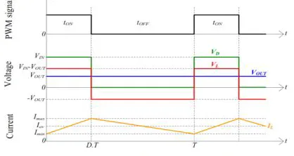
The Pulse Width Modulation (PWM ) is a technique in which a reference signal is coded into a pulse train whose widths correspond to the interpretation of the signal itself [6],[10]. The PWM requires two signals; the original signal, also called the “modulating signal”, which will be coded into a pulse train, and the “carrier signal”, which can be either a triangle wave or a saw-tooth wave. The resulted pulse train is called “modulated signal” which is the PWM signal itself. The PWM signal is generated by comparing the modulating signal with the high frequency carrier signal as depicted in Figure 1.
As can be seen in Figure 1, the PWM signal is made of rectangular pulses, which switch
between high and low levels. Figure 2 shows a close-up view of a sample PWM signal with a defining function y(t), period T, low level value ymin, high level value ymax, and a duty cycle D.
The average value of the PWM signal shown in Figure 2 can be expressed as
This relation reveals the direct dependence between the average value of the PWM signal and its duty cycle. The ability of controlling the average value of the PWM signal with its duty cycle creates many application areas for the PWM . The following sub-section summarizes some of the major application areas of the PWM .
Major Applications of Pulse Width Modulation
The pulse width modulation has been playing a critical role in many circuits and systems for a long time. Its unique structure makes the PWM participate in various applications. The major applications of the PWM can be listed as follows:
M otor Control
Available online: http://edupediapublications.org/journals/index.php/IJR/ P a g e | 927
value is adjusted to control the power delivered to a motor as it is expressed in (1). In PWM - controlled servomotors on the other hand, the servo position is determined by the width of the pulse instead of the duty cycle of the pulse. Controlling a servomotor with respect to the widths of the PWM signal is shown in Figure 3 with an example, where the servomotor used is HS-322HD of Hitec RCD, USA [13]. As can be seen in Figure 3, the specific values of the pulse widths of the PWM signal correspond to the specific rotation angles.
S witch-Mode Power S upplies
All electronic circuits and systems need power supplies to function. Power supplies can be categorized into two; linear power supplies and switch-mode power supplies (SM PS). Linear power supplies contain transistors working in the active operation region, causing high voltage drops at high currents. Thus, these types of supplies have large power dissipation resulting in low efficiency [10], [14].
SM PSs use transistors as switches in such a way that they allow current passing through them when they are “ON” and they do not conduct any current when they are “OFF”. For both cases, the power dissipation over the transistors are ideally zero. Therefore, the switch-type operation of the transistors dramatically reduces the power dissipation of the system resulting in a large improvement in the efficiency. High efficiency, small size and light-weight are the dominant characteristics of SM PSs over linear power supplies helping SM PSs employed in a variety of electronic systems such as personal computers, laptops, and televisions [15].
The PWM is an essential part of most of the SM PS circuits. Kazimierczuk in [10] defines a family of PWM -based circuits
consisting of the buck, boost, buck-boost, fly- back, forward, SEPIC (single-ended primary input converter), and dual SEPIC, which are all singleended types. M oreover, there are three multiple-switch PWM -based SM PS circuits such as the half-bridge, full-bridge, and push-pull converters. All of these circuits utilize the PWM in their control loop to adjust the output voltage. The detailed analysis of all PWM -based SM PS circuits are beyond the scope of this
work, however for the sake of
completeness, the PWM operation will briefly be covered for the buck and boost converter circuits. The circuit topology for the buck converter is shown in Figure 4.
Available online: http://edupediapublications.org/journals/index.php/IJR/ P a g e | 928
PROPOSED DPWM M ETHOD FOR
BACK-TO-BACK CONVERTERS A. Conventional PWM M ethods
Fig. 1 shows a typical circuit configuration of a back-to-back converter. The converter is composed of an input stage 3-phase AC power source, grid-side converter (VSC-1), motor-side converter (VSC-2), and a DC-Link capacitor, that is connected between them and an output stage 3-phase AC motor. Each VSC is formed by six power transistors and driven using pulse width modulation (PWM ). Sine pulse width modulation (SPWM ) and space vector pulse width modulation (SVPWM ) are the most commonly used modulation techniques due to their advantages such as implementation simplicity for the former and improved performance for the latter. The drawbacks of the SPWM are high level of total
harmonic distortion (THD), poor
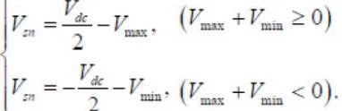
performance and over-modulation inability. All of them are overcome with the SVPWM method, by using modified sine-wave references. The reference voltage is obtained by adding a modified zero sequence component, usually referred to as an offset voltage into the phase voltage:
where Vas, Vbs, and Vcs are the phase
voltages, Vsn is the offset voltage, and Van,
Vbn, and Vcn are the reference voltages. The
offset voltage is obtained using the
maximum (Vm ax) and the minimum(Vm in)
values of the phase voltage references:
However, both SPWM and SVPWM methods applied to high-power VSCs, require the use of transistors with higher
Fig. 2. Reference voltage (Van), phase voltage (Vas), and offset voltage (Vsn) of
Phase A for different modulation schemes: (a) SPWM , (b) SVPWM , and (c) DPWM .
Available online: http://edupediapublications.org/journals/index.php/IJR/ P a g e | 929
highest, resulting in reduced switching loss for the designated interval, called a non-switching region. For three-phase PWM , the offset voltage should be selected that the reference voltages do not exceed the following limitations:
where Vdc is a DC-Link voltage.
Therefore, the offset voltage for the DPWM is obtained:
There is a variation of DPWM schemes, which can be applied by selecting corresponding offset voltages. The most commonly used one is a 60º DPWM , with the offset calculated as:
Fig. 2 provides phase voltage references and offset voltages of the aforementioned methods. Fig. 2(a) shows the SPWM waveform. As can be seen, there is no offset added to the reference voltage, so the reference voltage has a sine shape. The SVPWM reference voltage waveform is given in sine-shaped phase voltage. Finally, the waveform of the 60º DPWM method is shown in Fig. 2(c). As is evident, the reference voltage has regions, when the signal is clamped to either 0.5Vdc or – 0.5Vdc. During these moments, the corresponding transistors are not operated, and the switching loss are minimized.
B. Proposed DPWM M ethod
Although the conventional DPWM
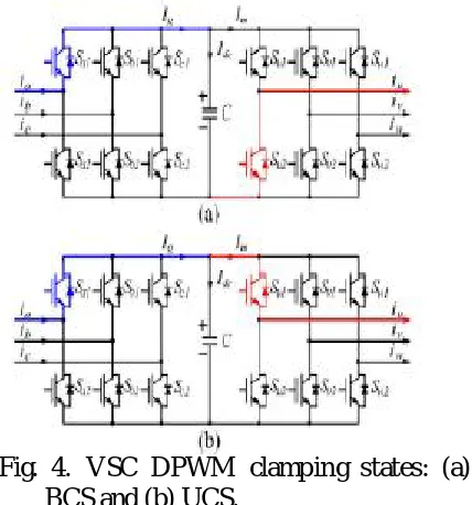
(CDPWM ) method has advantages in terms of cost and transistor loss reduction, there are other issues, which occur due to the reference signal being clamped either to positive or to negative DC-Link rail. In back-to-back topology, using DPWM methods causes the increase of the DC-Link current ripple. Fig. 3 shows the DC-Link current when the system is under the DPWM . The waveform, given in Fig. 3(a), describes the DC-Link current ripple of a bipolar clamping state (BCS), when two VSCs are clamped to opposite rails of the DC-Link. On the contrary, the waveform, shown in Fig. 3(b) depicts the capacitor current ripple in the case of a unipolar clamping state (UCS), in which both converters are clamped to the same rail of the DC-Link. Fig. 4 provides a circuit representation of these states. The BCS is shown in Fig. 4(a). The switches Sa1S and Su1 are clamped to the positive and the negative rails of the DC-Link, respectively. The UCS is given in Fig.4(b), where both switches Sa1 and Su1 are clamped to the same DC-Link rail.
Available online: http://edupediapublications.org/journals/index.php/IJR/ P a g e | 930
current can be determined as a superposition of phase currents of the VSC-1 (ia , ib , ic) and the VSC-2 (iu , iv , iw). It is known, that the sum of all three phase currents is 0, when their switching functions are at the same state:
where Sa, Sb, Sc, Su, Sv, and Sw are switching functions of the corresponding phases.
Fig. 5(a) shows the switching pattern and the DC-Link capacitor current ripple for the BCS. The transistors Sa1 and Su1 are clamped to the negative and to the positive DC-Link rails, respectively. Then, during the interval t0-t5, the transistors Sc1,Sb1, Sw1, and Sv1 are turned off sequentially.
Fig. 3. DC-Link current ripple of the DPWM : (a) BCS and (b) UCS.
Fig. 4. VSC DPWM clamping states: (a) BCS and (b) UCS.
By considering the currents and the switching states over each period of the intervals t0-t5 of Fig. 5(a), the instantaneous
value of the DC-Link current under the BCS for each period can be estimated as:
In the case of the UCS, shown in Fig. 3(b), Fig.4(b), and Fig. 5(b), the instantaneous value of the DCLink current is:
From Fig. 5, the ratio of the intervals T0, T1,
T2, T3, and T4 to the carrier period Ts for
Available online: http://edupediapublications.org/journals/index.php/IJR/ P a g e | 931
Fig. 5. PWM waveforms through one carrier period: (a) BCS, (b) UCS, and (c) SVPWM .
where va, vb, vc, vu , vv, and vw are the
reference voltage signals of phases a, b, c, u, v, and w, correspondingly, and Vdc is a
DC-Link voltage. In this paper, the reference voltage signals are represented as
where M1, ω1, Vsn1, M2, ω2, and Vsn2 are the
M I, fundamental angular frequency of the output voltages, and the offset voltages of
the VSC-1 and the VSC-2, respectively. The mean square value of the DC-Link current ripple over one carrier period can be calculated as:
Then for the BCS and the UCS the rms value of the DC-Link current ripple can be represented as:
Available online: http://edupediapublications.org/journals/index.php/IJR/ P a g e | 932
whereas the motor-side ac-current impacts on the negative ripple component. Thus, in the BCS, the DC-Link capacitor current
rapidly changes from the maximum
negative value to the maximum positive value, resulting in increased rms. On the other hand, as can be seen from (8) and (24), the DCLink capacitor current in the UCS is a superposition of the input and the output ac currents, where the currents of the clamped phases with the maximum values are subtracted from each other. Therefore, the maximum currents of the clamped phases do not result in the ripple component and the capacitor current is reduced for the UCS compared to that of the BCS. The rms value of the DC-Link capacitor in the case of the SVPWM is derived using the same principle as that of the BCS and the UCS.
The time interval ratios and the instantaneous current values can be find from Fig. 5(c). The final equation is given in (25). It can be seen, that similarly to the UCS, the instantaneous current values are subtracted from each other, therefore, the rms value of the current ripple is less than that of the DPWM under the BCS. In a DPWM -based back-to-back system, both the BCS and the UCS occur, causing the prominent current peaks of the DC-Link capacitor. Nevertheless, it is possible to curtail these current peaks by forcing the system to use only the UCS. It can be done by adjusting the offset voltage of both inverters and synchronizing the clamping regions and polarities. In this case, the offset voltage of the second VSC should be calculated considering the clamping periods of the first converter, which yields:
where Vmax.vsc1, Vmin.vsc1, Vmax.vsc2, and Vmin.vsc2 are the maximum and the
minimum values of phase voltage references of the VSC-1 and the VSC-2 respectively. Since the proposed DPWM (PDPWM ) method is derived the same way as the CDPWM , the maximum modulation index is the same for the CDPWM and the PDPWM and equals 1.15 for both methods. Fig. 6 provides the waveforms of phase voltage references, offset voltages, and reference voltages of the back-to-back
Fig. 6. The proposed DPWM method waveforms: (a) VSC-1 and (b) VSC-2.
Available online: http://edupediapublications.org/journals/index.php/IJR/ P a g e | 933
VSC-1, the reference voltage will differ for different speed of the motor.
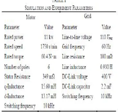
The simulation of the back-to-back converter was implemented by means of PSIM software to verify the efficiency of the proposed method. The circuit used for the simulation is the same with the one given in Fig 1. The simulation parameters are stated in Table I.
The motor is operated with 20 Nm load. The grid voltage is established at 110 Vrms with the frequency of 60 Hz. The DC-Link voltage is chosen to be 400 V. The DC-Link Capacitance is 2.2 mF. In a typical wind-turbine system, the frequency of the generator-side converter is usually set low to reduce the switching loss, while the grid-side converter frequency is chosen high for improving the current quality and reducing the grid filter size. However, for the proposed method, the switching frequency should be synchronized for both
III. SIM ULATION RESULT
Fig. 7. DC-Link current waveforms for the SVPWM method: (a) VSC-1 DC current, (b) VSC-2 DC current, and (c) DC-Link capacitor current.
Fig. 8. DC-Link current waveforms for the CDPWM method: (a) VSC-1 DC current, (b) VSC-2 DC current, and (c) DC-Link capacitor current.
converters. For the simulation, the switching frequency is set to 10 kHz for both VSCs.
Fig. 7 shows the DC-Link current ripple waveforms in the case when the VSC-1 and the VSC-2 are controlled using the SVPWM . The rms value of the DC-Link capacitor current is 4.22 A. The simulation results of the CDPWM are shown in Fig. 8. It can be easily observed that the DC-Link capacitor current is increased up to 5.33 Arms, although there is almost no change in the DC-Link current of the VSC-1 and the VSC-2.
Available online: http://edupediapublications.org/journals/index.php/IJR/ P a g e | 934
Fig. 9. DC-Link current waveforms for the PDPWM method: (a) VSC-1 DC current, (b) VSC-2 DC current, and (c) DC-Link capacitor current.
Fig. 10. Simulation waveforms of the CDPWM and the PDPWM : (a) DC-Link current ripple, (b) reference voltages of the VSC-1 and the VSC-2, (c) 3-phase output current, and (d) Common-mode voltage of the motor-side VSC.
CDPWM without a notable effect on the VSC-1 and VSC-2 DC currents. The DC-Link capacitor current ripple is reduced due to the elimination of the BCS, when the maximum current peak occurs. Instead, by matching the clamping states, it is possible to create conditions when the system has only the UCS. In this case, the DC-Link capacitor current ripple is even less as compared to the SVPWM .
Simulation waveforms of the CDPWM and the PDPWM methods are shown in Fig. 10. The prominent DC-Link current peaks, inherent to the CDPWM , are reduced with the proposed PDPWM method, as shown in Fig. 10(a). The reference voltages of both converters are given in Fig. 10(b). Obviously, after the proposed method is applied at 0.8 sec, the DC-Link
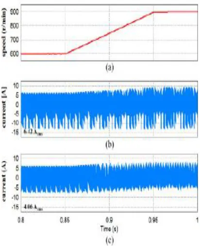
Fig. 11. The DC-Link capacitor current corresponding to the motor speed variation: (a) M otor speed, (b) CDPWM , and (c) PDPWM .
capacitor current ripple is reduced from 5.33 A to 3.78 A. In addition, as can be seen from Fig. 10(c), the proposed method slightly affects the THD level. The amplitude of the common-mode voltage, shown in Fig. 10(d) is not affected, when using the proposed method.
Available online: http://edupediapublications.org/journals/index.php/IJR/ P a g e | 935
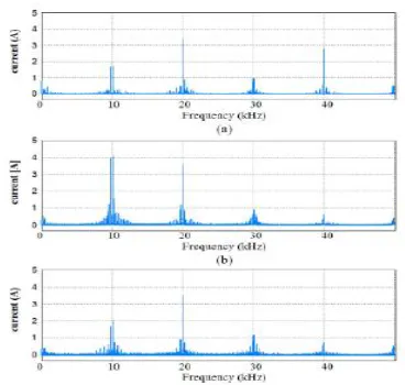
CDPWM and the DC-Link current ripple increases as the motor speed rises. On the other hand, using the PDPWM reduces the DC-Link current ripple and curtails the current peaks, as can be seen in Fig. 11(c). Fig. 12 shows the frequency spectrum of the DC-Link capacitor current for the SVPWM , the CDPWM , and the PDPWM . Obviously, the first order harmonic is the largest, when using the CDPWM and it is significantly decreased for the PDPWM method. The fourth order harmonic is similarly reduced, when using the CDPWM and the PDPWM compared to that of the SVPWM . The other harmonic components are similar for the three methods.
To estimate the efficiency improvement of the proposed method, the switching loss (PQ.sw) and the conduction loss (PQ.cond) of a transistor are calculated as:
where fsw is a switching frequency, EON is a
turn-on energy loss, EOFF is a turn-off energy loss, VCE is a collector-emitter voltage, IC is a collector current and Dsw is a duty ratio. The conduction (PD.cond) and
the switching loss (PD.sw) of a diode are
computed as:
where Err is a reverse recovery energy loss
of a diode, Vd is a diode voltage drop, IF is a
diode forward current, and DD is a
Fig. 12. Frequency spectrum of the DC-Link current: (a) SVPWM , (b) CDPWM , and (c) PDPWM .
Fig. 13. The total loss comparison between the SVPWM , the CDPWM , and the PDPWM methods at junction temperature 25˚C and 125˚C.
diode duty ratio. Fig. 13 provides the loss comparison between SVPWM , CDPWM and the PDPWM methods for two different M I of the VSC-1 at two different junction temperatures, 25˚C and 125˚C respectively.
Available online: http://edupediapublications.org/journals/index.php/IJR/ P a g e | 936
both DPWM methods compared to the SVPWM method
To further confirm the usefulness of the proposed method under different conditions, numerous simulations were implemented for various modulation indexes (M I) of the
Fig. 14. The DC-Link capacitor current comparison between SVPWM , CDPWM , and PDPWM for different M I.
Fig. 15. The THD comparison between SVPWM , CDPWM , and PDPWM for different M I.
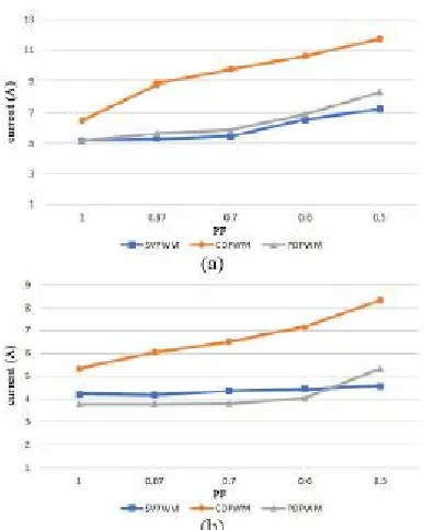
Fig. 16. The DC-Link capacitor current comparison between SVPWM , CDPWM , and PDPWM for different PF: (a) M I 0.9 and (b) M I 0.4.
Available online: http://edupediapublications.org/journals/index.php/IJR/ P a g e | 937
Fig. 17. The experimental set-up: (a) DSP Control boards, (b) Back-to- back converter set, and (c) M otor-load set.
Fig. 16. As is evident, the proposed method reduces the DC-Link capacitor current ripple compared to that of the CDPWM . However, with the higher M I, the performance of the proposed method decreases as the DC-Link capacitor current ripple level is higher compared to that of the
SVPWM . However, owing to such
advantages as the total loss minimization compared to that of the SVPWM and reduced DC-Link capacitor ripple in comparison to the CDPWM , the proposed method can be used as a tradeoff between the SVPWM and the CDPWM .
IV.EXPERIM ENTAL RESULTS
To ensure the feasibility of the proposed method, it was implemented in a laboratory using a twolevel back-to-back converter set shown in Fig. 17. The experimental circuit and parameters are identical to those used for the simulation and given in Table I. The VSC-1 and VSC-2 are controlled by two TM S320F28335 digital signal processor
(DSP) control boards. The IGBT switches used in the experimental setup are SK75M LI066T made by Semikron. The switching frequency is set to 10 kHz for both converters. The motor is operated at
600 r/min. Fig. 18 provides the
experimental waveforms of the DC-Link capacitor current ripple for the SVPWM , the CDPWM method and the PDPWM method. Evidently, all the waveforms are intimately matched with the simulation results. It can be clearly observed, that the ripple level is increased when using the CDPWM method, given in Fig. 18(b) as compared to the SVPWM shown in Fig. 18(a).
In addition, the current ripple of the DC-Link component is reduced for the PDPWM method as compared to both the SVPWM and the CDPWM , as can be observed from Fig
Available online: http://edupediapublications.org/journals/index.php/IJR/ P a g e | 938
Fig. 19. The experimental results: (a) BCS under the conventional DPWM and (b) UCS under the proposed DPWM .
18(c). Furthermore, as discussed in section II, the prominent current peaks occur when the clamping states of the converters are not matched and the system is under the BCS as shown in Fig. 19(a). The A-phase reference voltage of the VSC-1 is clamped to the positive DC-link rail, while the U-phase reference of the VSC-2 is clamped to the opposite side. This mismatch of the clamping states causes the current peaks of the DC-link capacitor. On the other hand, by applying the PDPWM method to the system, the DC-Link current peaks are
Fig. 20. The efficiency comparison between the SVPW M , the CDPWM , and the PDPWM for different
M I.
diminished with the clamping states of both converters being matched, as is evident from Fig. 19(b).
Therefore, the DC-Link current ripple is reduced from 5.5 A in the CDPWM to 3.7 A of the proposed method. Fig. 20 shows the
efficiency comparison between the
SVPWM , the CDPWM and the PDPWM . The efficiency is measured using Yokogawa WT3000 power analyzer. Obviously, the highest efficiency is obtained when using the CDPWM . In the case of the SVPWM , the efficiency is the lowest for all the M I. Finally, as can be seen from the graph, the efficiency of the proposed method is higher than that of the SVPWM . Therefore, in terms of the efficiency, the proposed method is a compromise between the SVPWM and the CDPWM .
CONCLUS ION
Available online: http://edupediapublications.org/journals/index.php/IJR/ P a g e | 939
switching devices endured less stress, when using the proposed method. This results in life-span expansion along with decreased size and cost of the whole system. On the other hand, one of the limitations of the proposed method is that the switching frequency of both converters should be the same, which is not typical for some applications, for example, the wind turbine systems. However, the proposed method can be effectively used in any other system, using the back-to-back topology.
REFERENCES
[1] Biman K. Bose, M odern Electronics and AC Drives. Upper Saddle River, NJ: Prentice-Hall,2001.
[2] A. Lega, S. M unk-Nielsen, F. Blaabjerg, and D. Casadei, “M ultilevel Converters for UPS Applications: Comparison and Implementation,” in Proc. European Conf. on Power Electron. and
Appl. (EPE), pp. 1–9, Sep. 2007.
[3] X. Jing, J. He, and N. A. O. Demerdash, “Application and Losses Analysis of
ANPC Converters in Doubly-Fed
Induction Generator Wind Energy Conversion System,” in Proc. IEEE International M achines and Drives Conf. (IEM DC), pp. 131–138, M ay. 2013.
[4] N. Huang, J. He, and N. A. O. Demerdash, “Sliding M ode Observer based Position Self-Sensing Control of a Direct-Drive PM SG Wind Turbine System Fed by NPC Converters,” in Proc. IEEE International M achines and Drives Conf. (IEM DC), pp. 919–925, M ay. 2013.
[5] J-H. Park and K-B. Lee, “Improved DPWM Scheme for Improvement of Grid Current Quality in a Large-Scale Grid-Connected Inverter System with a LCL-Filter,” in Proc. IEEE Energy Conversion Congr. and Expo. (ECCE), pp. 343–348, Sep. 2015.
[6] J-S. Lee, K-B. Lee, and F. Blaajberg, “Open-Switch Fault Detection M ethod of a Back-to-back Converter Using NPC Topology for Wind Turbine Systems,” IEEE Trans. Ind. Appl., Vol. 51, No 1, pp. 325–335, M ay. 2014. [7] F. Ueda, K. M atsui, M. Asao, and K.
Tsuboi, “Paralleled-Connections of Pulse Width M odulated Inverters Using Current Sharing Reactors,” IEEE Trans. Power Electron., Vol. 8, No. 2, pp. 185–193, Nov. 1993.
[8] L. Jatakas and W. Kaiser, “Low Harmonics, Decoupled Hysteresis Type Current Control of a M ulticonverter
Consisting of a Parallel
Transformerless Connection of VSC Converters,” in Proc. IEEE Ind. Appl. Society Conf. (IAS), pp. 1633–1640, Oct. 1997.
[9] R. Pena, J.C. Clare, and G.M . Asher, “Doubly Fed Induction Generator Using Back-to-back PWM Converters and its Application to Variable-Speed Wind-Energy Generation,” in Proc. IEEE Electr. Power Appl., Vol. 143, No. 3, pp. 231–241, M ay. 1996.
[10] H. Ye and A. Emadi, “An Interleaving Scheme to Reduce DC-Link Current Harmonics of Dual Traction Inverters in Hybrid Electric Vehicles,” in Proc. Appl. Power Electronics Conf. and Expo.(APEC), pp. 3205–3211, Nov. 2014.
[11] D. Zhang, F. Wang, and R. Burgos, “DC-Link Ripple Current Reduction for Paralleled Three-Phase Voltage-Source Converters With Interleaving,” IEEE Trans. Power Electron., Vol. 26, No. 6, pp. 1741–1753, Jun. 2011.
[12] H. Cai, R. Zhao, and H. Yang, “Study on Ideal Operation Status of Parallel
Inverters,” IEEE Trans. Power
Electron., Vol. 23, No. 6, pp. 2964– 2969, Nov. 2008.
Available online: http://edupediapublications.org/journals/index.php/IJR/ P a g e | 940
Inverters for Reactive Power and Harmonic Compensation,” in Proc. IEEE Power Electron. Spec. Conf. (PESC), pp. 1–7, Jun. 1997.
[14] Z. M . Ye, P. K. Jain, and P. C. Sen, “Circulating Current M inimization in High Frequency AC Power Distribution Architecture with M ultiple Inverter M odules Operated in Parallel,” IEEE Trans. Ind. Electron., Vol. 54, No. 5, pp. 2673–2687, Oct. 2007.
[15] G. Gohil, R. M aheshwari, L. Bebe, T. Kerekes, R. Teodorescu, M . Liserre,
and F. Blaabjerg, “M odified
Discontinuous PWM for Size
Reduction of the Circulating Current Filter in Parallel Interleaved Converters,” IEEE Trans. Power Electron., Vol. 30, No. 7, pp. 3457– 3470, Jul. 2015.
[16] J-H. Park, H-G. Jeong, and K-B. Lee, “An Improved DPWM M ethod for Reduction of Resonant Problem in the Inverter,” in Proc. IEEE Energy Conversion Congr. and Expo. (ECCE), pp. 1528–1533, Sep. 2014.
[17] Y. Bak and K-B. Lee, “Discontinuous PWM for Low Switching Losses in Indirect M atrix Converter Drives,” in Proc. Appl. Power Electronics Conf. and Expo. (APEC), pp. 2764–2769, M ar. 2016.
[18] S-A. Lee, S-W. Hyun, and C-Y. Won, “The M ethod of DPWM Injected Offset Voltage for Control of Neutral Point Voltage Using 3-Level NPC Inverter,” in Proc. ITEC Conf., pp. 317–321, Jun. 2016.
[19] L. Asiminoaei, P. Rodriguez, and F.
Blaabjerg, “Application of
Discontinuous PWM M odulation in Active Power Filters,” IEEE Trans. Power Electron., Vol. 23, No. 4, pp. 1692-1706, Jul. 2008.
[20] J-H. Kim, S-K. Sul, H. Kim, and J-K. Ji, “A PWM strategy for four-leg
voltage source converters and
applications to a novel line interactive UPS in a three-phase four-wire
system,” in Proc. IEEE Ind.
Appl.Society Conf. (IAS), pp. 2202-2209, Oct. 2004.
[21] D-W. Chung and S-K. Sul, “M inimum-Loss Strategy for Three-Phase PWM Rectifier,” IEEE Trans. Indust. Electron., Vol. 46, No. 3, pp.517–526, Jun. 1999.
[22] I. Jlassi, J. O. Estima, S. K. El Khil, N. M . Bellaaj, and A. J. M . Cardoso,
“M ultiple Open-Circuit Faults
Diagnosis in Back-to-Back Converters of PM SG Drives for Wind Turbine
Systems,” IEEE Trans. Power.
Electron., vol. 30, no. 5, pp. 2689-2702, M ay 2015.
[23] U-M . Choi, H-H. Lee, and K-B. Lee, “Simple Neutral-Point Voltage Control for Three-Level Inverters Using a
Discontinuous Pulse Width
M odulation,” IEEE Trans. on Energy Convers., Vol. 28, No. 2, pp. 434–443, Jun. 2013.
[24] T. Khani and M . Patt, “DC-Link Harmonic Content in Double Two-Level Inverter for Permanent M agnet Synchronous M otor Drive Systems – Comparison and Analysis,” in Proc. Power Conversion and Intell. M otion Conf. (PCIM ), pp. 2122–2128, M ay. 2016.
[25] J-S. Lee and K-B. Lee, “Open-Switch Fault Tolerance Control for a Three-Level NPC/T-Type Rectifier in Wind Turbine Systems,” IEEE Trans. Ind. Electron., vol. 62, no. 6, pp. 1012-1021, Feb. 2015.
[26] S. Bernet, “Recent Developments of High Power Converters for Industry and Traction Applications,” IEEE Trans. Power Electron., Vol. 15, No.6, pp. 1102–1117, Nov. 2000.
[27] T. Thacker, R. Burgos, F. Wang, and
D. Boroyevich, “M inimum Loss
Available online: http://edupediapublications.org/journals/index.php/IJR/ P a g e | 941
Voltage Source Converters,” in Proc. Center Power Electron. Syst. Semin. (CPES), pp. 469–502, Oct. 2008.
[28] L. Dalessandro, S.D. Round, U.
Drofenik, and J. W. Kolar,
“Discontinuous Space-Vector
![Fig. 1. Circuit configuration of a back-to-back converter. effective in wind energy conversion systems and traction power systems mostly owing to the capability of the bidirectional power flow [8]–[10]](https://thumb-us.123doks.com/thumbv2/123dok_us/1882746.1245437/1.595.315.514.498.580/circuit-configuration-converter-effective-conversion-traction-capability-bidirectional.webp)