A Low-Power Integrated Smart Sensor with on-Chip
Real-Time Image Processing Capabilities
Massimo Barbaro
Department of Electrical and Electronic Engineering, University of Cagliari, Piazza d’Armi, 09123 Cagliari, Italy Email:[email protected]
Luigi Raffo
Department of Electrical and Electronic Engineering, University of Cagliari, Piazza d’Armi, 09123 Cagliari, Italy Email:[email protected]
Received 16 September 2003; Revised 13 May 2004
A low-power, CMOS retina with real-time, pixel-level processing capabilities is presented. Features extraction and edge enhance-ment are impleenhance-mented with fully programmable 1D Gabor convolutions. An equivalent computation rate of 3 GOPs is obtained at the cost of very low-power consumption (1.5µW per pixel), providing real-time performances (50 microseconds for overall com-putation, 0.5 GOPs/mW). Experimental results from the first realized prototype show a very good matching between measures and expected outputs.
Keywords and phrases:smart sensors, bioinspired circuits, real-time image processing.
1. INTRODUCTION
Real-time, low-power, low-cost, and portable vision systems apt to be adopted as an optical front end on mobile and autonomous systems are more and more demanded for by the consumer electronic market. Specific vision tasks, rang-ing from segmentation to recognition (characters, faces, pos-tures, obstacles) and classification, are required in several dif-ferent applications which are emerging from the needs of the automotive, mobile surveillance market. In the automotive field, for example, an increasing number of electronic devices are being introduced in the car to improve safety and ability. Sensors will be needed for applications such as drive-support and safety measures. In the mobile market, more and more capabilities (such as OCR, face recognition and so on) will be built in the 3G cell phones, which are already being equipped with digital cameras. Surveillance systems repre-sent an exploding market with plenty of complex image pro-cessing applications, such as biometric identification in air-ports, to cite only one. Promising fields of application are also medical assistance and, of course, robotics.
These applications (requiring estimation of motion-in-depth, computation of time-to-contact, target tracking, ob-ject recognition, and other high-level image processing tasks) are examples ofperceptive tasks, or problems conveying the necessity of taking a quick decision on the basis of a sensory input (visual, in this case). The traditional approach to image
processing, based on acquisition on a CCD camera and soft-ware processing on a digital platform (PC, DSP, or ASIC), has proven to be scarcely fit to accomplish perceptive tasks. In fact, even if a wide and reliable collection of software algo-rithms is available and computational capabilities of digital platforms are constantly evolving and improving, neverthe-less, it seems that the constraints of real time, low cost, low power and portability can be hardly contemporaneously met with the classic approach. Need for low-power operations as well as real-time requirements overwhelms performances of classic imager/PC systems thus requiring a different ap-proach.
At the same time, unfortunately, there are several drawbacks: reduction of image resolution, increase of device dimensions, and critical design issues. Thus, it is clear that the develop-ment of a smart system is intimately related to the specific application it can encompass and the adoption of this pro-cessing paradigm requires a proper evaluation of the tradeoff between cost, design time, speed, power consumption, and versatility of the device.
2. RELATED WORKS AND MOTIVATION
Starting with the seminal work of Mead [2], at Caltech, a large number of different vision sensors were proposed in the literature. Most of these sensors are somehow inspired by biology and try tomorphthe structure of vertebrate retina. A number of vision chips implement low-level spatial pro-cessing, such as normalization and contrast sensitivity [3], normalization and high-pass spatial filtering [4], detection of preferred orientations [5], and extraction of contrast direc-tion and magnitude [6]. Others are more oriented to a time-domain processing such as the imager from Tobi Delbruck [7], which adopts a self-adaptive photosensor altogether with a time-derivative processing, or the insect’s vision-based sen-sor from Moini [1] capable of detecting direction and veloc-ity of motion of objects, or the temporal difference imager described in [8] or in [9]. More specialized vision sensors implement sophisticated and mixed spatio-temporal pro-cessing, like the retina from Etienne-Cummings [10] which implements target tracking within a foveated approach or, again, the steerable spatiotemporal imager described in [11], or the low-power orientation selective chip from Shi [5]. These latter systems are more oriented to a generic bioin-spiration and the electronic implementation is not so closely related to biological counterparts but inspired by biological architectures or algorithmic solutions.
In this paper, we present a novel, low-power CMOS im-age sensor which entails, at pixel level, real-time filtering capabilities. Low-level image processing is implemented by means of massively parallel analog computing cells inte-grated into the photodiodes. With respect to other vision chips, we focused our attention on meeting, at the same time, low-power, medium-resolution, and real-time constraints. Moreover, with respect to other sophisticated and special-ized chips, we chose to implement a kind of image process-ing (Gabor filter) which is very versatile and useful for a large set of different high-level algorithms (seeSection 3). A prototype version of the chip was realized and successfully tested.Section 3presents the sensor capabilities and the im-plemented algorithm. The chip architecture is described in
Section 4 while Section 5 covers the circuit design of each block.Section 6discusses test setup and results andSection 7
draws the conclusions.
3. SMART SENSOR
The choice of the proper algorithm is crucial for the success-ful design of a smart vision system. In this paper, we present
x(n)
y(n)
Figure1: Connection scheme for noden.
a device capable of convolving the acquired image with a Gabor-like function kernel, whose mathematical 1D expres-sion is the following:
h(n)=Ce−λ|n|cos(ωn+φ). (1)
It has been shown that Gabor convolution is an ideal low-level processing task that can be useful for a large number of different applications. They range from stereo depth esti-mation [12,13] to motion detection [14,15,16,17], texture analysis [18,19], segmentation [20,21,22], and estimation of motion-in-depth [23]. Key feature for all these algorithms is the possibility of interactively changing the parameters of the kernel (frequency of the cosine, decaying factor of the ex-ponential gain). Very fast output rate is required to be able to perform multiscale and multifrequency filtering of the same image.
As stated in [24], the convolution between the input im-age and a Gabor-like kernel can be obtained introducing lin-ear interactions between the pixels, as shown inFigure 1. The connection scheme is described, in mathematical form, by
a2y(n−2)+a1y(n−1)+a0y(n)+a1y(n+1)+a2y(n+2)=x(n),
(2)
where x(n) is local luminance input at pixeln, y(n) is the filter output and the value of coefficientsa0,a1, anda2
com-pletely determines the shape of the kernel (C,λ, andω in (1)), while the phaseφcan be set linearly combining the out-puts [25]. We call this basic analogue convolverperceptual engine. It is worthy to note that, to obtain stable and oscillat-ing kernels, coefficientsa2anda1must have opposite signs.
The circuit implementation of the perceptual engine is pro-vided in detail inSection 5.2. The main drawback of Gabor filters is their sensitivity to background illumination due to their nonzero mean value, therefore, circuitry for removal of the mean output value is needed. This circuitry is described inSection 5.3.
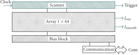
4. CHIP ARCHITECTURE
Clock
Scanner Trigger
Array 1×64 Iout
Ismooth
Bias block
Communication Com Figure2: System overview of the realized chip: main blocks.
4.1. Pixel array
The core block is, of course, the array of pixels, made up of a 1D array of 64 pixels tightly interconnected one with the other. This block has two outputs: an output current (Iout),
which is the result of the convolution of the input image with the kernel, and an average current (Ismooth), which is
the smoothed (low-pass filtered) version of the output cur-rent. The smoothing is programmable and the average can be local or global. The two output currents can be subtracted one from the other simply connecting together the two out-put pins (the currents have opposite sign). Both currents are available off-chip in order to be able to turn on and offthe edge-enhancing high-pass filter. In this way, it is possible to enhance information coming from edges and get rid of the Gabor kernel mean output value, which is the main draw-back of Gabor filters, as explained inSection 3.
The single pixel is divided into three main blocks which perform different tasks. The overall structure is depicted in
Figure 3. The first block is devoted to signal acquisition and conditioning. Light is converted into a current and this cur-rent is globally normalized in order to be sure that operating conditions of further stages are within safety ranges.
The second block implements the convolution (percep-tual engine), so it is the counterpart of the single cell depicted inFigure 1. Basically, this block generates weighted replicas of output current necessary to implement (2) and provides them to the first and second neighbors on the left and on the right (S(n−1),S(n−2),S(n+ 1), andS(n+ 2), respectively). Weightsaiare electrically set to choose the proper kernel. Bi-ases are needed to set the parameters of the filter and con-tributions from the neighboring pixels are summed at node S(n) to correctly implement (2). The output of this stage is a current (PE current) representing the convolution of the in-put image with the perceptual engine.
The third block is made up of a selection block with a smoothing filter that can be tuned or even disabled. The out-put current coming from the previous block is replicated and connected by means of a switch to a global output node di-rectly attached to a pin. The switch is turnedONby the sig-nal sel(n) coming from the scanner. The replica of the out-put current is smoothed with a lowpass filter and connected to another global output node by means of another switch driven by the inverted signalnsel(n). The output currents coming directly from the perceptual engine and smooth-ing filter are available at the same time off-chip but the two
output pins can be shorted to obtain their difference (edge-enhanced version of the image).
4.2. Scanner circuitry, bias block, and communication block
The scanner is needed to access in a raster way each pixel of the array. It is realized as a standard ring counter made-up of foundry standard cells.
An analog bias block is needed to generate all the bias signals exploited by the circuitry in the pixel (such asvr,v1, v2, and so on). To simplify testing and control of the device, these biases are generated internally by means of 11 digital-to-analog converters with current output. The 11 DACs con-tain digital registers accessible from off-chip via an SPI proto-col. So, each bias can be set digitally writing the correct value in the proper register. In this way, we are able to program fre-quency, envelope, and gain of the Gabor kernel as well as to-tal output current (INORM), amount of the smoothing per-formed on the image and some other control parameters.
Finally, a communication block is needed to interface the device with a PC to download the proper settings and inter-actively change the parameters of the kernel. The commu-nication block implements a standard SPI interface through which the content of each register is set.
5. CIRCUIT IMPLEMENTATION 5.1. Acquisition and conditioning
The acquisition and conditioning block is shown in
Figure 4a. The light-to-current transducer is a photodiode obtained with N-well to P-substrate junction. Despite of its slightly bulkier area, this photodiode was preferred with respect to other solutions, such as N-diffusion over P-substrate, in order to collect a larger number of photons in the visible spectrum thanks to its deeper junction position. A better absorption coefficient is needed since the process-ing circuitry reduces the area of the photodiode, reducprocess-ing its sensitivity.
Global normalization is achieved by means of a circuit described elsewhere (see [26, 27]) based on a translinear loop (transistors MNI andMNO). Basically, global nodes VNORM and INORM are common to all the pixels. In this way, the sum of all output currents IPHN(n) is set to INORM. The translinear loop forces currents ofMNI and MNO to be proportional, soIPHN(n) = kIPH(n). Thus, if total input current isITOTAL, the output current of this block is
IPHN(n)=ITOTALIPHINORM (n). (3)
Global
biases Selection
From neighbors AV (n) Vlat Vver Sel (n) nSel (n) AV (n+ 1) To neighbors
Global biases
Vbias INORM VNORM
Acquisition and conditioning
Smoothing and selection
Iout
Ismooth
Global outputs
IPHN(n) PE current
Vr
V1
V2
V3 Sign!
Perceptual engine
To neighbors S (n−1)
S(n−2)
S(n) From neighbors
S(n+ 1)
S(n+ 2) To neighbors
Figure3: System overview of the realized chip: pixel structure.
± VDD2 ↓ ITOTAL
VNORM (global) INORM (global)
IPH(n) MNI MNO
A(n) IPHN(n)
Vbias
Ib MN1 MN2
(a)
PE current
nsel (n)
Iout
Ismooth
sel (n)
MN1 MP1
MSWP
MSWN
MP2 AV (n)
MVER
MN2
Vlat MLAT
AV (n+ 1) Vver
(b)
Figure4: Circuit details of the pixel:(a) acquisition and conditioning; (b) output stage and smoothing filter.
affected. On the other side, the current should not become too low in order to grant a good signal-to-noise ratio. Dark current noise is always present in a photodiode and the sig-nal current should always be sufficiently higher in order to be distinguished from noise.
5.2. Basic circuit: perceptual engine
M2L M32 M31 M21 MR1 M12
M2R M11 PE current (n)
S(n−2) S(n+ 2) IPE(n)
v3 v2 vr v1
M3 M2 MR M1
Sign! Msign
S(n)
M33 1 : 2 M34 ↓ IPHN(n)
S(n−1)S(n+ 1)
M1L
M13 M1R
Figure5: Circuit diagram for the single pixel. NodeS(n) is the node where all contributions are summed and (2) is carried out.
neighbors; at the same time, weighted contributions from neighbors and local input are collected and summed exploit-ing Kirchoffcurrent law (KCL).
Core processing unit is made up of transistorsMR,M1,
M2, and M3. These MOS transistors generate the weighted
copies; they are biased and sized in order to work in their weak inversion region (but in saturation) and can be de-scribed aspseudoconductances[28]. The sum is implemented at nodeS(n) where all currents converge.
Since the core block is basically a programmable current divider, its functionality can be described writing all currents, except input current, in terms of the output currentIPE(n), which flows inMR. In fact,
IM1=G
∗
1
G∗
RIPE, IM2=
G∗
2
G∗
RIPE, IM3=
G∗
3
G∗
RIPE, (4)
whereG∗R,1,2,3=(Is/V0)e(VR,1,2,3−VT0)/(nUT)is the programmable pseudoconductanceofMR,1,2,3, depending only on process pa-rameters and gate voltage.
Current generator labelledIPHN(n) represents the out-put of the acquisition and conditioning block, currents com-ing from neighborcom-ing pixels are injected at nodeS(n) where the KCL equation becomes
G∗
2
G∗
RIPE(n−2)−
G∗
1
G∗
RIPE(n−1)+
G∗
R+G∗1+G∗2±G∗3
G∗
R IPE(n)
±G∗1
G∗
RIPE(n+ 1) +
G∗
2
G∗
RIPE(n+ 2)=Iin(n) +Ib.
(5)
Thus, (5) represents the implementation of (2), where Iin(n) corresponds tox(n),IPE(n) toy(n), and
a0=1 +G
∗ 1 G∗ R + G∗ 2 G∗ R ± G∗ 3 G∗
R =1 +
I1REF
IRREF
+ I2REF IRREF ±
I3REF
IRREF
,
a−1=a1= −G
∗
1
G∗
R = −
I1REF
IRREF
, a−2=a2=G
∗
2
G∗
R =
I2REF
IRREF.
(6)
The constant bias currentIb, added to the photodiode cur-rent in the previous block, shifts the zero level of the output current preventing the filter from being saturated by negative current peaks.
Since the value ofGR,1,2,3is determined by gate voltages,
thepseudoconductancesand, consequently, theaiparameters and shape of the filter can be easily set adjusting four ref-erence currents (I(R, 1, 2, 3)REF) flowing in diode-connected
transistors in a global bias block ofFigure 2.
Contributions from thenth pixel to the first and second neighbors are provided through current mirrors M1∗ and M2∗. The proper sign fora1anda2coefficients is obtained
by a sequence of odd or even mirroring of the current. Signal
signand transistorsM3∗are adopted to increase the range of programmability of coefficients, selecting the minus or plus sign in (6).
Since the whole processing is kept local and does not de-pend on any process parameter (which are canceled in the ratios of matched components), the circuit is robust with re-spect to parameters’ fluctuations and mismatch. In fact, all matched transistors are within the same pixel and can be laid out in a very compact area.
5.3. Output stage and smoothing filter
The third block composing the pixel is shown inFigure 4b. The gate voltage PE current, coming from the output current mirror of the perceptual engine is applied to the input tran-sistorMP1 (output stage of a current mirror) and generates a replica of the output current. This current is injected in a first-order diffusive network made up of transistorsMLAT andMVER. The idea is the same described in [26], a slight amount of the current is lost through the lateral connec-tions while the remaining flows inMVER. In fact, transistor MLATis connected to the first neighbor on the right through pin AV(n+ 1), while pinAV(n−1) connects the pixel to its first neighbor on the left. The output smoothed current has an opposite sign with respect to the real output cur-rent, so it can be easily subtracted (to perform edge enhance-ment) just connecting nodesIoutandIsmooth. The smoothing
Bias
Analog array
(a) (b)
Figure6: Layout and dimensions of the realized chip: (a) microphotograph of the chip; (b) pixel layout: with respect to the chip micropho-tograph, the layout is rotated 90 degrees.
and then performing the edge enhancement is equivalent to performing the enhancement and then the Gabor convolu-tion. Only, in the first case, we can use just one Gabor filter while in the latter we would have needed two different Gabor filters (one for the image and one for its smoothed version).
6. EXPERIMENTAL RESULTS AND DISCUSSION 6.1. Integration
A prototype device with an array of 1×64 pixels was realized in an analog 0.5µCMOS process from Alcatel Mietec with double-poly three metals, and a hipo resistor. Dimensions of the single pixel are 33µm×245µm for an area of about 8000µm2 and a fill factor of about 11%: these dimensions
are compatible with the integration of low-cost, medium-sizesmartdevices (over 10 000 pixels).Figure 6ashows a mi-crophotograph of the chip, whileFigure 6bshows the layout of a single pixel.
With respect to other implementations such as [5], our device is based on a very compact circuit able to implement the Gabor convolution with 18 transistors only. With 13 tran-sistors more, also normalization and high-pass filtering (not available in the previously cited work) were implemented.
6.2. Real time
Computing time of the filter depends only on the time re-sponse of the single pixel since filtering is performed in par-allel by all pixels at the same time. Time response is dom-inated by the integrating node S(n) where all currents are summed. This node is a low-impedance node (looking into the source terminals ofMR,M1,M2, andM3) with a low
ca-pacitance due only to parasitic caca-pacitances of sources and drains.Figure 7shows simulations result for a transient anal-ysis of the circuit. Output currents (here we plotIoutand not
its high-pass filtered version just to show the range of varia-tion of real currents flowing in the circuit) of all 64 pixels are shown for a step input current of 5 nA (going from 10 nA to 15 nA). Computation time can be estimated in 50 microsec-onds with output currents in the order of 50 nA. Increasing current level, of course, decreases propagation delay but in-creases power consumption.
6.3. Power consumption
In the proposed simulation, power consumption can be esti-mated summing up the currents flowing in all the branches of the perceptual engine fromVDD to ground. This static component of power is the dominant one, in this circuit,
4.6e−08 4.5e−08 4.4e−08 4.3e−08 4.2e−08 4.1e−08 4e−08 3.9e−08 3.8e−08 3.7e−08 3.6e−08
(
A
)
0 2e−05 4e−05 6e−05 8e−05 0.0001 Time (s)
Figure7: Transient response of the perceptual engine: output cur-rent (Iout) versus time for an input curcur-rent step going from 0 to 5 nA at timet=10 microseconds.
since dynamic power is wasted mainly to change voltage at node S(n). In fact, voltage atS(n) determines all the out-put currents since the gate voltages ofM1,M2,M3, andMR
are constant. These transistors are biased in weak inversion, so their transconductance is very large and only very small changes in voltages are needed to obtain large changes in currents. For this reason, dynamic power is very small, com-pared to static one. There are 9 branches for a total current of around 450 nA in the central pixel. This current means a power consumption of 1.5µW for the central pixel.
A rough comparison with a digital approach can be done calculating the equivalent computation rate of the circuit. A possible digital implementation of the Gabor filter requires an FIR spatial filter with at least 20 taps. Implementing this filter with a DSP would require 20 multiplications (one for each tap) and 19 sums. If each operation requires only an instruction, the total number of instructions needed to per-form convolution of an image of 64×64 pixels would be (20 + 19)×642. Performing the overall filtering in 50
5.5 5 4.5 4 3.5 3 2.5 2 1.5 1
Vout
(
V
)
0 10 20 30 40 50 60 70
Pixel (a)
5.5 5 4.5 4 3.5 3 2.5 2 1.5 1
Vout
(
V
)
0 10 20 30 40 50 60 70
Pixel (b) 6
5.5 5 4.5 4 3.5 3 2.5 2 1.5 1
Vout
(
V
)
0 10 20 30 40 50 60 70
Pixel (c)
5 4.5 4 3.5 3 2.5 2 1.5 1
Vout
(
V
)
0 10 20 30 40 50 60 70
Pixel (d)
Figure8: Several kernels implemented by the realized device: experimental data (∗) versus expected results (solid). Starting from the top left and clockwise: (a) kernel 1 (λ1 =0.496,ω1 =0.9,C1 =1), (b) kernel 2 (λ2 =0.449,ω2 =1.1,C2 =0.6), (c) kernel 3 (λ3 =0.496, ω3=1.3,C3=0.8), and (d) kernel 4 (λ4=0.449,ω4=1.5,C4=0.8).
6.4. Accuracy
Precision of the circuitry is mainly affected by mismatches in the core transistors of the perceptual engine (MR, M1,
M2, and M3). In fact, those transistors are biased in
weak-inversion and are sensitive to fluctuations of threshold volt-age. For this reason, to set theW/Lof the core transistors, we adopted a design strategy based on minimization of expected SNR of the final result, described in [30] which maximized accuracy of the device. InFigure 8, the experimental results with 4 different kernels corresponding to different combina-tions of frequency, envelope, and gain are shown. It is wor-thy to note the very good matching between expected results (calculated Gabor-like functions obtained from the model) and experimental data.
Programmability and precision of the device are proven by the fact that measurements fit very well expected wave-forms. Accuracy was measured by calculating the SNR for each test (seeFigure 9). Signal-to-noise ratio was computed subtracting experimental results and expected results to ob-tain noise. Power of both signal and noise was calculated
and the corresponding SNR computed. Results are SNR1 =
26 dB, SNR2 = 25 dB, SNR3 = 35 dB, and SNR4 = 32 dB (kernels 1, 2, 3, and 4 are those of Figure 8, from top left and clockwise). It is worth to note that expected results are calculated with the Gabor-like formula and not from circuit simulations.
These data were obtained exciting the network with a current impulse in the central pixel and converting output current into a voltage off-chip. A fixed pattern noise of the order of 15% of bias currentIb, mainly due to the way this bias current is generated on-chip, affects the performances of the chip but it can be systematically corrected simply sub-tracting the noise image from signal image. This FPN is due to a problem in the layout of the bias transistors and will be amended in future implementations.
7. CONCLUSIONS
4500 4000 3500 3000 2500 2000 1500 1000 500 0
P
o
w
er
d
ensit
y
sp
ect
rum
0 10 20 30 40 50 60 70
Frequency
Figure9: Power density spectrum of both expected data (+) and experimental results (∗) for kernel 1.
Table1: Chip characteristics.
Technology 0.5µm Alcatel Mietec
Resolution 1×64 pixels
Chip area 3.5 mm×1.6 mm
Pixel area 33µm×245µm
Transistors per pixel 31
Fill factor 11%
Static power consumption 1.5µW per pixel
Processing time 50µs
Computational capabilities 3 GOPs
kernel has been conceived, designed, realized, and tested. The chip is versatile, programmable, and useful for a range of embedded applications requiring small area, low power, and very fast image processing. The overall convolution is led on in less than 50 microseconds for a step change in in-put current. This delay does not depend upon the resolution of the device since it is mainly due to the time response of the circuit of the single pixel. Power consumption is slightly dependent on the implemented kernel since changes in pa-rameters ai imply a large range of variation for the pseu-doconductancesG∗R,1,2,3. However, for the single pixel, it can always be kept under 1.5µW.Table 1 summarizes the chip characteristics.
An equivalent computation rate of 3 GOPs is obtained by means of a full parallelism implemented at pixel level. The bidimensional version of the chip can be easily obtained by replicating the 1D array.
ACKNOWLEDGMENT
The authors wish to thank Michele Ancis and Federico Cabiddu for their contribution.
REFERENCES
[1] A. Moini, Vision Chips, Kluwer Academic Publishers, Nor-well, Mass, USA, 2000.
[2] C. A. Mead,Analog VLSI and Neural Systems, Addison-Wesley Publishing, Boston, Mass, USA, 1989.
[3] A. G. Andreou and K. A. Boahen, “A 590,000 transis-tor 48,000 pixel, contrast sensitive, edge enhancing, CMOS imager-silicon retina,” inProc. 16th Conference on Advanced Research in VLSI (ARVLSI ’95), pp. 225–240, Chapel Hill, NC, USA, March 1995.
[4] P. Venier, “A contrast sensitive silicon retina based on con-ductance modulation in a diffusion network,” inProc. 6th In-ternational Conference on Microelectronics for Neural Networks and Fuzzy Systems (MicroNeuro ’97), pp. 163–173, Dresden, Germany, September 1997.
[5] B. E. Shi, “A low-power orientation-selective vision sensor,” IEEE Transactions on Circuits and Systems II: Analog and Dig-ital Signal Processing, vol. 47, no. 5, pp. 435–440, 2000. [6] P.-F. Ruedi, P. Heim, F. Kaess, et al., “A 128×128 pixel
120-dB dynamic-range vision-sensor chip for image contrast and orientation extraction,” IEEE J. Solid-State Circuits, vol. 38, no. 12, pp. 2325–2333, 2003.
[7] T. Delbruck and C. A. Mead, “Analog VLSI adaptive loga-rithmic wide-dynamic-range photoreceptor,” inProc. IEEE International Symposium on Circuits and Systems (ISCAS 94), vol. 4, pp. 339–342, London, UK, May-June 1994.
[8] V. Gruev and R. Etienne-Cummings, “A pipelined temporal difference imager,” IEEE J. Solid-State Circuits, vol. 39, no. 3, pp. 538–543, 2004.
[9] S.-Y. Ma and L.-G. Chen, “A single-chip CMOS APS cam-era with direct frame difference output,” IEEE J. Solid-State Circuits, vol. 34, no. 10, pp. 1415–1418, 1999.
[10] R. Etienne-Cummings, J. Van der Spiegel, P. Mueller, and M. Z. Zhang, “A foveated silicon retina for two-dimensional tracking,” IEEE Transactions on Circuits and Systems II: Ana-log and Digital Signal Processing, vol. 47, no. 6, pp. 504–517, 2000.
[11] V. Gruev and R. Etienne-Cummings, “Implementation of steerable spatiotemporal image filters on the focal plane,” IEEE Transactions on Circuits and Systems II: Analog and Dig-ital Signal Processing, vol. 49, no. 4, pp. 233–244, 2002. [12] T. D. Sanger, “Stereo disparity computation using Gabor
fil-ters,”Biol. Cybern., vol. 59, pp. 405–418, 1988.
[13] B. Crespi and G. Tecchiolli, “Adaptive Gabor filters for phase-based disparity estimation,” Int. J. Pattern Recogn. and Artif. Intelligence, vol. 13, no. 5, pp. 591–614, 1999.
[14] G. M. Bisio, L. Raffo, and S. P. Sabatini, “Analog VLSI primi-tives for perceptual tasks in machine vision,”Neural Comput-ing Applications, vol. 7, pp. 216–228, 1998.
[15] E. A. Vittoz and X. Arreguit, “Systems based on bio-inspired analog VLSI,” inProc. 5th International Conference on Micro-electronics for Neural Networks and Fuzzy Systems (MicroNeuro ’96), Lausanne, Suisse, February 1996.
[16] C. W. G. Clifford, J. N. Freedman, and L. M. Vaina, “First and second-order motion perception in Gabor micropattern stimuli psychophysics and computational modeling,” Cogni-tive brain research, vol. 6, no. 4, pp. 263–271, 1998.
[17] T. Nagano, M. Hirahara, and W. Urushihara, “A general model for visual motion detection,” inProc. 9th IEEE Interna-tional Conference on Neural Information Processing (ICONIP ’02), vol. 1, pp. 149–152, Piscataway, NJ, USA, November 2002.
[19] D. A. Clausi and M. E. Jernigan, “Designing Gabor filters for optimal texture separability,”Pattern Recognition, vol. 33, no. 11, pp. 1835–1849, 2000.
[20] J. H. Van Deemter and J. M. Hans du Buf, “Simultaneous detection of lines and edges using compound Gabor filters,” Int. J. Pattern Recogn. and Artif. Intelligence, vol. 14, no. 6, pp. 757–777, 2000.
[21] L. Wiskott, “Segmentation from motion: combining gabor and mallat-wavelets to overcome the aperture and correspon-dence problems,”Pattern Recognition, vol. 32, no. 1, pp. 1751– 1766, 1999.
[22] A. K. Jain and N. K. Ratha, “Object detection using Gabor filters,”Pattern Recognition, vol. 30, no. 2, pp. 295–309, 1997. [23] S. P. Sabatini, F. Solari, P. Cavalleri, and G. M. Bisio, “Phase-based binocular perception of motion-in-depth: cortical-like operators and analog VLSI architectures,” EURASIP Journal on Applied Signal Processing, vol. 2003, no. 7, pp. 690–702, 2003.
[24] L. Raffo, S. P. Sabatini, G. Bo, and G. M. Bisio, “Analog VLSI circuits as physical structures for perception in early visual tasks,” IEEE Trans. Neural Networks, vol. 9, no. 6, pp. 1483– 1494, 1998.
[25] L. Raffo, “Analysis and synthesis of resistive networks for dis-tributed visual elaborations,”Electronics Letters, vol. 32, no. 8, pp. 743–744, 1996.
[26] E. A. Vittoz, “Analog VLSI signal processing: why, where and how?,”Journal of VLSI Signal Processing, vol. 8, no. 1, pp. 27– 44, 1994.
[27] E. A. Vittoz, “Pseudo-resistive networks and their applications to analog collective computation,” inProc. 6th International Conference on Microelectronics for Neural Networks and Fuzzy Systems (MicroNeuro ’97), vol. 1327, pp. 1133–1150, Dresden, Germany, September 1997.
[28] E. A. Vittoz and X. Arreguit, “Linear networks based on tran-sistors,”Electronics Letters, vol. 29, no. 3, pp. 297–299, 1993. [29] http: // dspvillage.ti.com/docs/allproducttree.jhtml? pageId=
C5.
[30] M. Barbaro and L. Raffo, “Design of an analog front-end de-vice for low-level image processing,” inProc. 15th Conference on Design of Integrated Circuits and Systems (DCIS ’00), pp. 832–835, Montpellier, France, November 2000.
Massimo Barbaroreceived the M.S. and the Ph.D. degrees fron University of Cagliari in 1997 and 2001, respectively. He joined the Department of Electrical and Electronic En-gineering, University of Cagliari, Italy, in 2002, as an Assistant Professor. His research activity is in the field of low-power analog COMS integrated sensores and vision chips