Low Power and Low Area Master Slave
Match Line Design for Content Addressable
Memory
K. Chaitanya Lakshmi 1, G. Mary Sowjanya 2
P.G. Student, Department of Electronics and Communication Engineering, VR Siddhartha Engineering College,
Kanuru, Vijayawada, India1
Assistant Professor, Department of Electronics and Communication Engineering, VR Siddhartha Engineering College,
Kanuru, Vijayawada, India 2
ABSTRACT: Content Addressable Memory (CAM) is a special type of hardware storage mostly designed for fast lookup applications. It can perform an associative search operation within one clock cycle. However, the parallel search scheme costs the CAM memory large power consumption. In this paper, we tend to propose a new CAM architecture, called Master–Slave Match Line (MSML) design, that aims to mix the master–slave architecture and charge refill reduction technique to reduce the CAM power dissipated within the match lines (MLs). Unlike the conventional design, wherever one single ML is employed, our design uses one master-ML (MML) and a number of other slave-MLs (SMLs) to carry out the search operation. By sharing the MML charge with merely the mismatched SML, this MSML design can diminish the MML charge refill swing, such that the Match line power consumption can be reduced efficiently. In addition, we further propose a modified 4T-CAM Cell and replace the basic 9T CAM Cell with the modified 4T CAM Cell and propose an MSML Design to reduce the power and area.
KEYWORDS: Charge refill minimization, content-addressable Memory (CAM), low-power, master–slave architecture, Match Line (ML).
I. INTRODUCTION
Low power consumption has become the new metrics for decisive the performance of an electronic device. Several electronic systems such as laptop computers and mobile phone have become a commodity and a necessity. Because the demand for portable applications will increase the demand for extended utilization and higher processing speed of the system also will increase. Content Addressable Memory (CAM) is a different kind of memory employed in terribly high-speed search applications largely used as a Translation Lookaside Buffers (TLB). The TLB permits the interpretation of the virtual address of a CPU to a physical address used in a cache memory. Each CAM and Static Random Access Memory (SRAM) share several functionalities and similarities. Content Addressable Memory (CAM) is a special type of associate memory that outgrows from the existing RAM technology. It provides the same basic features such as “read” and “write”, and offers an on-chip parallel search capability against the data contents. Hence, it is appropriate to refer CAM as a hardware “search engine”. It can perform an associative search operation within one clock cycle, which is not always possible for Random Access Memory (RAM).
II. BASIC CONTENT ADDRESSABLE MEMORY
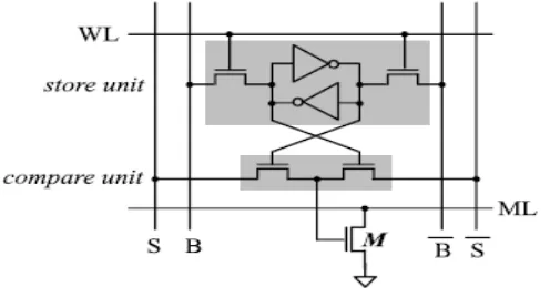
Each CAM Cell as shown in Fig. 1 have two parts: 1) bit storage component (e.g. 6T SRAM) and 2) bit comparison circuit. The bit storage component is used to store input data, and the bit comparison circuit (a pass transistor logic PTL) is applied to compare a preferred search data with the stored data. The most frequently used CAMs are binary CAM (BCAM) cell and ternary CAM (TCAM) cell. Due to the frequent search and also the parallel comparison feature wherever an outsized quantity of transistors and wires are active on every search, the power consumption of CAM is usually extensive. In the CAM memory, the match lines (MLs) and search lines (SLs) are the major power consumers. The ML is the long wire with massive capacitance, and every search will cause a huge amount of ML switching activities. Thus, the ML power consumption is very large.
Fig 1. The Basic structure of XOR CAM cell.
The match line scheme is one of the key factors for CAM circuit design. Traditionally, two match line schemes are usually used in CAMs. One is NOR-type, the other is a NAND - type. The characteristic of NOR-type is high-speed but heavy power consumption. The advantage of the NOR type CAM is its best search performance due to single NMOS pull down path. But due to the highly capacitive nature of match line the power consumed is HIGH in this array. The advantage of the NAND-type CAM is the low power consumption in the match case as the match line is less capacitive in nature and power consumed in discharging is less in match case. However, one of the disadvantages is that the match line path is too long to discharge to the ground when there is match case.
III.PREVIOUS ARCHITECTURES
Fig 2. SMA proposed in [5]
In [5], the segmented ML architecture (SMA) was proposed. As shown in Fig. 2, the SMA partitions the whole ML into four segments. These four segments are grouped into the precharged type and the charge-shared type. First, only the precharged segments are charged, and then the charge spread signal is enabled during the match evaluation phase. This results in the charge sharing occurred between the charge shared segment and the precharged segment. Because only the precharge segments need to be charged, the ML power consumption can be efficiently reduced. Fig. 3 shows the shadow ML design [6], which is mainly composed of the level shifter (LS) and voltage detector (VD). In the evaluate phase, VD is used to charge the ML and sense the shadow ML voltage at the same time. In the case of a mismatch, at least one path between the ML and shadow ML conducts.
Fig 3 Shadow ML Voltage detecting Scheme [6]
IV. MSML DESIGN
The key idea behind our design is to mix the master–slave architecture with the charge refill minimization method to diminish the ML switching power. Fig. 6 shows an MSML design example, MS2, that consists of one MML and two SMLs. As a result of sharing the charge between the MML and the SML, we can minimize the MML refill swing efficiently, such that the search power dissipated within the MMLs can be mainly reduced. From Fig. 4, besides the MML and SML, an additional final-ML (FML) is employed to specify the match result. Note that the parasitic capacitance of the FML is generally smaller than that of the MML.
Search Operation
Similar to the standard CAM, in our design, there are two phases during a search. They are precharge and match evaluation phases, respectively. In the precharge phase, the MML and FML are initially precharged to high, and then during the match evaluation phase only the mismatch case will change the logic level of the FML from high to low. 1. Precharge Phase
During this section, the control signal PRE is high. Thus, the MML and FML are precharged to high, and all SMLs, i.e., SML1 and SML2 shown in Fig. 4, are discharged to 0. As the result of the search data are not available in this phase, all BLs (bit and ∼bit) are reset to 0, such that the XOR result is 0 to turn OFF the share transistor (Mx). Thus, the charge sharing paths between MML and SML, i.e., S1 and S2, are all disconnected in this phase.
2. Match Evaluation Phase
Fig. 4. MSML design configured with two SMLs.
the SML1 and SML2 are matched. The key node voltage and path connection/disconnection for these cases are summarized in Table 1, and the complete operation is described as follows.
Case 1 (Both SML1 and SML2 are Match)
This is only the match case. In this case, both the charge sharing paths S1 and S2 do not conduct. All ML logics are the same as in the precharge phase, i.e., MML is 1, FML is 1, and both SML1 and SML2 are 0.
Case 2 (Either SML1 or SML2 is Mismatch)
We first assume that SML1 is a mismatch, and SML2 is matched. In the SML1 phase, as a result of a minimum of one share transistor is turned ON to conduct the charge-sharing path S1, the MML charge will be distributed to the SML1. This leads to an increase of the SML1 voltage, whereas the MML voltage level goes down. After the entire charge sharing, both the MML and SML1 will finally saturate to the equivalent voltage, i.e., Final balance voltage. According to the charge sharing equation, the final balance voltage VB can be derived as follows:
VB= CMML / (CMML + CSML1)VMML≈ 2/3VMML (1)
Where CMML and CSML1 are the capacitances of MML and SML1, respectively, and VMML is that the MML initial voltage. Because the MML capacitance is roughly two times the SML1 Capacitance, the result can be simplified as 2/3VMML.
Table I Key node voltage and node connection or disconnection (O/X) for each case in the MSML design
Case 3 (Both SML1 and SML2 are Mismatch)
In this case, both SML1 and SML2 segments are mismatch. Because the charge-sharing path S1 and S2 are conducted, the MML charge is going to be distributed to the SML1 and SML2. For MS2 configuration, this is the worst case. The final balance voltage VB can be derived as follows:
VB= CMML / (CMML + CSML1 + CSML2)VMML≈ 1/2VMML (2) Cases SML1 SML2 Path Key Node Voltage Result
S1 S2 P MML SML1 SML2 FML Case1 Match Match X X X VDD 0 0 VDD Match
Case2 Mismatch
Match Mismatch
Mismatch 0
X X
0 0
0
VDD
VDD
VDD
0
0
VDD 0
0
Mismatch
Mismatch
V. PROPOSED 4T CAM AND MSML DESIGN
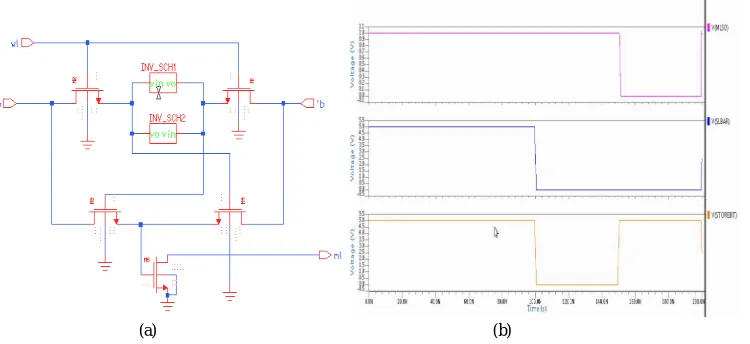
The proposed CAM design utilizes a special type of CAM cell. However, rather than utilizing ancient Basic CAM cell
configuration, the modified CAM cell contains only four transistors as shown in Fig 6(a). The four-transistor (4-T) content addressable memory (CAM) cell consists of an exclusively n - type transistors This cell has two transistors (Tc1 and Tc0) arranged in an exclusive-OR configuration so as to perform a comparison between the information given at the BIT and NBIT lines and data stored in the cell.
Table II Match operation of 4T CAM.
The match line is directly connected to the output of the exclusive-OR (XOR). Consequently, the condition of this line relies on the XOR output. This XOR is generated by transistors Tc1 and Tc0. If the XOR output is at logic level “1”, the match line Will not be discharged to 0, showing that a match has been found. On the other hand, if the output of XOR is at logic level “O”, the match line gets discharged, showing a non-matching condition.
VI.SIMULATIONRESULTS
The circuits are drawn and simulated using MENTOR GRAPHICS Pyxis Schematic Editor tool and the technology used here is 130nm. Simulation is done using Eldo simulator. The output waveforms are viewed using an E-Z wave viewer.
(a) (b)
Fig. 5. Basic XOR CAM (a) Schematic Of 9T CAM (b) Simulation result of 9T CAM cell search operation
The matching operation of the XOR CAM cell includes comparing the data displayed on the bit lines (BIT and NBIT lines) to Stored
data
Sb1 Sb0 BIT NBIT Match condition
0 0 1 0 1 Match
0 0 1 1 0 No match
1 1 0 1 0 Match 1 1 0 0 1 No match
the stored data and assessing the match line. The match line is precharged to logic level “1” before comparing the stored data with the input. Since the output of the XOR is associated to match the line, when there is a mismatch between the stored data and the input, the output of XOR is set to logic level “0”. This, in turn, discharges the match line. If a match is found, then the output of exclusive-OR is set to logic level “1”. So, there is no discharge of the match line. The operation remains same in 4T CAM cell only difference is reduced number of transistors.
Fig. 6. 4T XOR CAM (a) Schematic Of Modified 4T XOR CAM (b) Simulation result of 4T XOR CAM cell
In this project we are replacing the basic 9T CAM Cell with that of the modified 4T CAM Cell in MSML design and its results have been compared.
(a) (b)
(c)
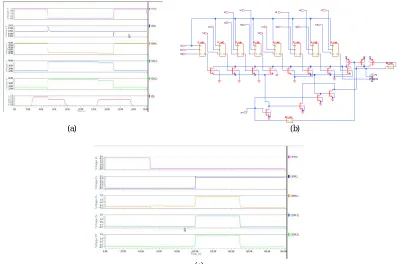
Fig. 7. (a) Simulation result of 8- bit MSML design of 9T CAM cell (b) Schematic of 8- bit MSML design of 4T CAM cell (c) Simulation result of 8- bit MSML design of 4T CAM cell
Here, the MSML used is MS2 configuration i.e. one Master with two slaves. By sharing the MML charge with merely the mismatched SML, this MSML design can diminish the MML charge refill swing, such that the Match line power consumption can be reduced efficiently.
(a) (b)
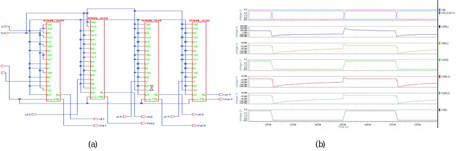
Fig. 8. (a) Schematic of 32- bit MSML design of 4T CAM cell (b) Simulation result of 32- bit MSML design of 4T CAM cell
VII. POWER CONSUMPTION AND DELAY
Match line and search lines are highly capacitive in nature. So the major portions of power consumed in CAM are due to search lines switching i.e. search lines discharge to the ground in precharge phase and during the evaluation phase one of the search line pairs is high.
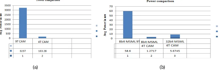
Table III Comparison of 9T CAM and 4T CAM
CAM POWER DELAY POWER DELAYPRODUCT
9T XOR CAM
3.237mw 5.9ps 1.9057*10-14J
4T XOR CAM
163.28uw 65.5ps 1.0694*10-14J
Table III and IV Summarizes the simulation results of the above circuits. It is observed that the power of the 4 transistor CAM cell is reduced than that of the power of the 9 transistor CAM cell. But the delay of 4T CAM cell is more than that of the 9T CAM cell.
Table IV Comparison of various MSML designs
DESIGN POWER 8 BIT MSML DESIGN OF 9T
XOR CAM
58.632mw
8 BIT MSML DESIGN OF 4T XOR CAM
1.2717mw
32 BIT MSML DESIGN OF 4T CAM CELL
(a) (b)
Fig. 9. (a) Power Comparison of 9T CAM and 4T CAM(b) Power Comparison of various MSML designs
From this comparison result, we can say that as the number of transistors reduced the power will also be reduced. In MSML design also the power will be reduced with the decrease in a number of transistors.
VIII. CONCLUSION
This paper introduces a Low power ML design, called MSML design, in which we mix the master–slave architecture with the charge refill minimization technique to reduce the CAM ML power consumption. Here, various MSML designs are compared and observed that the proposed 4T CAM Cell and MSML design of the 4T CAM cell have less Power and hence used in fast lookup applications. By replacing the 9T CAM cell with the 4T CAM cell the area is also reduced because the transistor count reduced.
REFERENCES
[1] Yen-Jen Chang, Member, IEEE, and Tung-Chi Wu “Master–Slave Match Line Design for Low-Power Content-Addressable Memory” IEEE Transactions. Very Large Scale Integr. (VLSI) Syst.,Vol. 23, no. 9, September 2015.
[2] Yen-Jen Chang and Yuan Hong Liao “Hybrid-type CAM design for both power and performance efficiency in VLSI systems”, Vol No: 8, Aug 2008
[3] K. Pagiamtzis and A. Sheikholeslami, “Content addressable memory (CAM) circuits and architectures: A tutorial and survey,” IEEE J. Solid-state Circuits, Vol. 41, no. 3, pp. 712–727, Mar. 2006.
[4] H. Miyatake, M. Tanaka, and Y. Mori, “A design for high speed lowpower CMOS fully parallel content-addressable memory macros,” IEEE J. Solid-state Circuits, vol. 36, pp. 956–968, June 2001.
[5] S. Baeg, “Low-power ternary content-addressable memory design using a segmented match line,” IEEE Transactions Circuits Syst. I, Reg. Papers, Vol. 55, no. 6, pp. 1485–1494, Jul. 2008.
[6] J. Zhang, Y. Ye, and B. Liu, “A new mismatch-dependent low power technique with shadow match-line voltage-detecting scheme for CAMs,” in Proc. ACM/IEEE Int. Symp. Low Power Electron. Design, Oct. 2006, pp. 135–138.
[7] K. H. Cheng, C. H. Wei, and S. Y. Jiang, “Static divided word matching line for low-power content addressable memory design,” in Proc. Int. Symp. Circuits Syst., May 2004, pp. 629–632.
[8] K. Pagiamtzis and A. Sheikholeslami, “A low-power content-addressable memory (CAM) using pipelined hierarchical search scheme,” IEEE J. Solid-state Circuits, vol. 39, no. 9, pp. 1512–1519, Sep. 2004.
[9] I. Arsovski, T. Chandler, and A. Sheikholeslami, “A ternary contentaddressablememory (TCAM) based on 4T static storage and including a current-race sensing scheme,” IEEE J. Solid-state Circuits, vol. 38, no. 1, pp. 155–158, Jan. 2003.
[10] N. Mohan and M. Sachdev, “Low-capacitance and charge-shared match lines for low-energy, high-performance TCAMs,” IEEE J. Solid-state Circuits, vol. 42, no. 9, pp. 2054–2060, Sep. 2007.
[11] Xiao-Liang Tan, Anh-Tuan Do, Shou-Shun Chen, Kiat-SengYeo, Zhi-Hui Kong “A New Match line Sensing Technique in Content Addressable Memory IEEE COOL Chips XIV 2011.
[12] H.-Y. Li, C.-C. Chen, J.-S. Wang, and C. Yeh, “An AND-type matchline scheme for high-performance energy-efficient content addressable Memories,” IEEE J. Solid-state Circuits, vol. 41, no. 5, pp. 1108–1119, May 2006.
![Fig 2. SMA proposed in [5]](https://thumb-us.123doks.com/thumbv2/123dok_us/1631139.1203348/3.595.182.416.404.486/fig-sma-proposed-in.webp)