Design A Multiplier Using Reversible Gates Shift Register
Kallagunta Anil & M.Rambabu1M.tech-Scholar, Dept of ECE, Chebrolu Engineering College, Guntur, A.P, India
2Associate Professor, Dept of ECE, Chebrolu Engineering College, Guntur, A.P, India
ABSTRACT: This paper proposes a low-power and area-efficient shifter design using reversible logical gates. The area and power consumption are reduced by replacing flip-flops with pulsed latches. This method solves the timing problem between pulsed latches through the use of multiple non-overlap delayed pulsed clock signals instead of the conventional single pulsed clock signal. The shift register uses a small number of the pulsed clock signals by grouping the latches to several sub shifter registers and using additional temporary storage latches. Here the reversible gate designs called NSG. The purpose of NSG is to implement in all logical Boolean operations. The reversible gates that perform reversible logic synthesis are Feynman gate, toffoli gate, fredkin gate, peres gate etc., and some of other reversible gates. By using these reversible N.S gate we make a multiplier that gives very efficient output.
Index Terms—area-efficient, flip-flop, pulsed clock, pulsed latch, shift register.
I.INTRODUCTION
In VLSI circuit the basic building block is the shift register. Many applications such as communication receivers, image processing ICs and digital filters are used by the shift registers. Due to the high demand for high quality image data continues to increase. To process large image data in image processing ICs the word length of the shift register must be increases. A 4k-bit shift register is used by an image extraction and vector generation VLSI chip. 2K-bit shift register is used by a10-bit 208 channel output LCD column driver IC. 45K-bit shift register is used by a 16-mega-pixel CMOS image sensor.
When the word length of shift register increases, the area and power consumption of the shift register become important design considerations.
The architecture of a shift register is very simple. An N-bit shift register is composed of N data flip-flops which are connected in series. The speed of the flip-flop is less important because there is no circuit between the flip-flops in the shift register. To reduce the area and power consumption in shift register it is suitable to use smallest flip-flop. Recently, in many applications flip-flops are replaced by pulsed latches because a pulsed latch is much smaller than a flip-flop. Due to the timing problem between pulsed latches, the pulsed latch cannot be used in a shift register.
By using multiple non-overlap delayed pulsed clock instead of the conventional single pulsed clock signal the shift register solve the timing problem. By grouping the latches to several sub shift registers the shift register uses a small number of the pulsed clock signals and using a additional temporary storage latches.
Fig. 1.(a) Master-slave flip-flop. (b) Pulsed latch.
Fig. 1(a) shows a master-slave flip-flop using two latches can be replaced by a pulsed latch consisting of a latch and a pulsed clock signal in Fig. 1(b). For the pulsed clock signal all pulsed latches share the pulse generation circuit. Then the area and power consumption of the pulsed latch become almost half of those of the master-slave flip-flop. For small area and low power consumption the pulsed latch is an attractive solution.
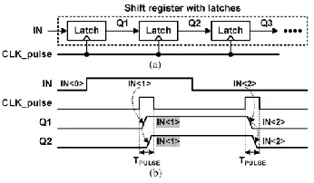
Fig. 2. Shift register with latches and a pulsed clock signal. (a) Schematic. (b)
Waveforms.
Due to the timing problem the pulsed latch cannot be used in shift registers as shown in Fig.2. In Fig. 2(a) the shift register consists of several latches and a pulsed clock signal (CLK_pulse). In Fig. 2(b) the operation waveforms shows the timing problem in the shifter register. Because the input signal of the first latch (IN) is constant the output signal of the first latch (Q1) changes correctly during the clock pulse width (TPULSE). During the clock pulse width its input signal (Q1) changes then the second latch has an uncertain output signal (Q2).
Fig 3. Shows One solution for the timing problem is to add delay circuits between
latches. The output signal of the latch is
delayed (T DELAY ) and reaches the next latch
after the clock pulse. During the clock pulse
width (TPULSE ), the output signals of the first
and second latches (Q1 and Q2) changes. But after the clock pulse the input signals of the second and third latches (D2 and D3) become the same as the output signals of the first and second latches (Q1 and Q2). As a result during the clock pulse, all latches have constant input signals and no timing problem occurs between the latches.
Fig. 3. Shift register with latches, delay circuits, and a pulsed clock signal. (a)
Schematic. (b) Waveforms.
Schematic. (b) Waveforms.
Fig 4(a). Shows the multiple non-overlap delayed pulsed clock signals which is the another solution. When a pulsed clock signal goes through delay circuits the delayed pulsed clock signals are generated. Each latch uses a pulsed clock signal which is delayed from the pulsed clock signal used in its next latch. As a result, during its clock pulse each latch has a constant input and no timing problem occurs between latches. This solution also requires many delay circuits.
To reduce the number of delayed pulsed clock signals the existed shift register is divided into M sub shifter registers. A 4-bit sub shifter register consists of five latches. It performs shift operations with five non-overlap delayed pulsed clock signals.
.
III.PROPOSED SHIFTER DESIGN USING REVERSIBLE LOGICAL
GATES
A Reversible logic gate is an input and n-output logic device with one-to-one mapping. This helps to determine the inputs which can be uniquely recovered from the outputs and also the outputs from the inputs. Also direct fan-Out is not allowed as one-to-many concept is not reversible in the synthesis of reversible circuits. However by using additional gates fan-out in reversible circuits is achieved. By using minimum number of reversible logic gates a reversible circuit should be designed.
Without the use of any sequential logic a Barrel shifter can shift a data word by a
specified number of bits only in
pure combinatorial logic. One way to
implement it as a sequence
of multiplexers where the output of one multiplexer is connected to the input of the next multiplexer in a way that depends on the shift distance. Typically within a single clock cycle a barrel shifter is often used to shift and rotate n-bits in modern microprocessors.
A logic component that perform shift or rotate operations is a Barrel Shifter. For digital signal processors the Barrel shifters
are applicable. Depending on the
instantiation parameters the component design is for a natural size (4,8,16…) barrel shifters that perform shift right logical, rotate right, shift left logical, and rotate left operations. Through inversion of the input and output vectors the left and right operation is implemented, so the basic multiplexing function can perform both operations. The number of multiplexing stages is relative to the input vector width.
A combinational logic circuit in which k select lines controls the bit shift operation with n-inputs and n-outputs is the Barrel shifter. Barrel shifter can be unidirectional which provides data to be rotated or shifted in both the directions allowing data to be shifted only to left (or right), or bi-directional. A barrel shifter which is having n inputs and k select lines is known as (n,k) barrel shifter.
stage either shifts over 2i bits or leaves the data unchanged. A logarithmic barrel shifter of each stage is controlled by a control bit.
Reversible barrel shifter can perform six operations, they are logical right shift, arithmetic right shift, right rotate, logical left shift, arithmetic left shift and left rotate.
Logical Right Shift: A 3-bit logical right shift operation right shifts the input data by 3 bits and sets the leftmost 3-bits to zero.
Arithmetic Right Shift: A arithmetic right shift operation right shifts the input data bit by 3-bits and sets the leftmost 3-bits to the sign bit.
Right Rotation: A right rotation operation performs a right shift operation on input data by 3-bits
Logical Left Shift: A 3-bit logical left shift operation left shifts the input data by 3-bits and sets the right most 3-bits to zero.
Arithmetic Left Shift: In the arithmetic left shift operation the remaining bits are logically left shifted by 3-bits and the sign bit of the input data remains intact.
Left Rotation: A left rotation operation performs a left shift operation on input data by 3-bits. Further the rightmost 3-bits are set to the leftmost 3-bits of the original input data.
The reversible barrel shifters have considered the number of garbage outputs, the number of ancilla inputs, and the quantum cost as the parameters to be
optimized. The functional verification of the reversible design methodologies for the barrel shifters are done in Verilog HDL.
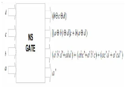
FIG 5. REVERSIBLE NS GATE
Fig 5. Shows the reversible NSG gate. In this reversible NSG gate the input pattern analogous to a particular output pattern can be exclusively determined. The input d, c, b and a are termed as input terminal 1, 2, 3 and 4 respectively and the output are termed as output 1, output 2, output3 and output 4 respectively.
The multiplier, adder and
register/accumulator are used in MAC unit. We used a 8 bit modified Reversible NS multiplier. From the memory location the MAC inputs are obtained and given to the multiplier block. This will be useful in 8 bit digital signal processor.
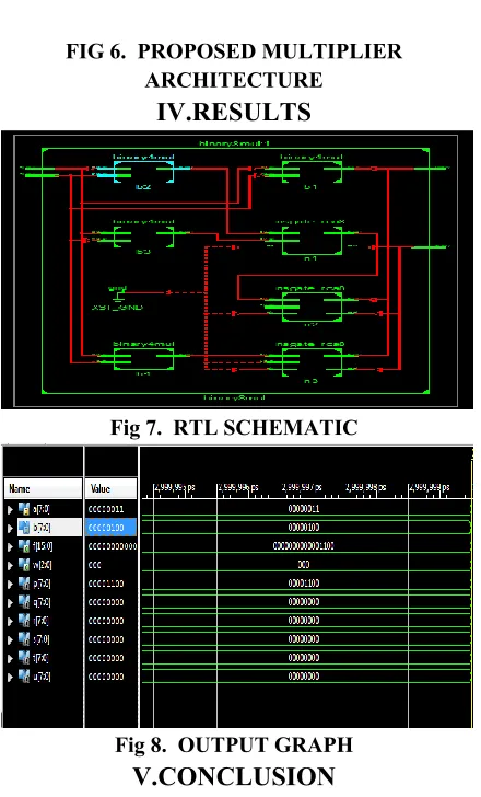
FIG 6. PROPOSED MULTIPLIER ARCHITECTURE
IV.RESULTS
Fig 7. RTL SCHEMATIC
Fig 8. OUTPUT GRAPH
V.CONCLUSION
A low-power and area-efficient shifter design using reversible logical gates is proposed. The shift register reduces area and power consumption by substituting flip-flops with pulsed latches. The timing
problem between pulsed latches is solved using multiple non-overlap delayed pulsed clock signals as an alternative of a single pulsed clock signal. This paper proposed an approach to realize the multipurpose binary reversible gates. Such gates can be used in regular circuits for realizing Boolean functions. In the similar way it is possible for constructing multiple -valued reversible gates which having the similar properties. 8*8 multiplication is realized with reversible NSG gate in an appropriate and enhanced manner. This unique approach multiplier is applicable for multipurpose applications in all domains.
VI.REFERENCES
[1] P. Reyes, P. Reviriego, J. A. Maestro, and O. Ruano, “New protection techniques against SEUs for moving average filters in a
radiation environment,” IEEE Trans. Nucl.
Sci., vol. 54, no. 4, pp. 957–964, Aug. 2007.
[2] M. Hatamian et al., “Design
considerations for gigabit ethernet 1000
base-T twisted pair transceivers,” Proc.
IEEE Custom Integr. Circuits Conf., pp.
335–342, 1998.
[3] H. Yamasaki and T. Shibata, “A real-time image-feature-extraction and vector-generation vlsi employing
arrayed-shift-register architecture,” IEEE J. Solid-State
Circuits, vol. 42, no. 9, pp. 2046–2053, Sep.
2007.
[4] H.-S. Kim, J.-H. Yang, S.-H. Park, S.-T. Ryu, and G.-H. Cho, “A 10-bit column-driver IC with parasitic-insensitive iterative
charge-sharing based capacitor-string
interpolation for mobile active-matrix
LCDs,” IEEE J. Solid-State Circuits, vol.
[5] S.-H. W. Chiang and S. Kleinfelder, “Scaling and design of a 16-megapixel
CMOS image sensor for electron
microscopy,” in Proc. IEEE Nucl. Sci.
Symp. Conf. Record (NSS/MIC), 2009, pp.
1249–1256.
[6].NM Nayeem, MdAHossian, L Jamal and Hafiz Md. HasanBabu, “Efficient design of Shift Registers using Reversible Logic,” Proceedings of International Conference on Signal Processing Systems, 2009.
[7].Samir palnitkar, “verilog HDL”, second edition, IEEE 1364-2001 compliant.
[8].J. E. Rice, “A New Look at Reversible Memory Elements,” Proceedings of IEEE International Symposium on Circuits and Systems, 2006.
[9].H. Thapliyal and M. B. Srinivas, “A Beginning in the Reversible Logic Synthesis of Sequential Circuits,” Proceedings of Military and Aerospace Programmable Logic Devices International Conference, 2005.
KALLAGUNTA ANIL completed
his B.Tech in Pace institute of technology and sciences, Ongole and pursuing M TECH in Chebrolu Engineering College, Guntur.
M.RAMBABU, pursuing his Ph.D
from Sunrise University, Alwar, M.Tech at SRKR engineering college, Bhimavaram and B.Tech at Newton's engineering college, Macherla, Guntur. At present he is working as Associate professor at
Chebrolu Engineering College,