327 |
P a g e
HIGH PERFORMANCE AND LOW POWER
ASYNCHRONOUS DATA SAMPLING WITH POWER
GATED DOUBLE EDGE TRIGGERED FLIP-FLOP
1
R.Ramya,
2C.Hamsaveni
1,2
PG Scholar, Department of ECE, Hindusthan Institute Of Technology, Coimbatore.(India)
ABSTRACT
Power consumption and energy efficiency is a major role in sequential circuit design. Power gating is a
technique that is used to reduce the static power consumption of idle modules. Usage of Dual Edge Triggered
Flip-flop (DETFF) is an efficient technique since it consumes the clock frequency and less power than Double
Edge Triggered Flip-flops (DETFF’s). Integrating power gating technique with DETFF reduces the power
consumption and leakage power further, but it leads to asynchronous data sampling problem. In this paper, two
methods have been used to eradicate the asynchronous data sampling problem and their power analysis has
been estimated. In order to reduce the leakage power consumption further, a new design has proposed for a
DETFF. Based on his new design, the two methods have been implemented using 130 μm Tanner EDA tool.
Keyword
:
Double Edge Trigger Flip Flop, Clock Gating, Power Gating, Single Edge trigger Flip
Flop
.
I. INTRODUCTION
Power efficiency and energy savings are considered to be vital issues for designers. Normally, high-performance
chips will have high clock frequency, which leads to high power consumption. Therefore, less power consuming
designs are needed.
The major source of power consumption in a sequential circuit is clock tree and the timing components. Higher
speed of clock, increase level of integration and technology scaling are reasons for high increases in power
consumption. Therefore low power consumption is becoming very crucial factor for VLSI circuits. Performance
assessment of the SVM showed leak size, location is both predicted with a reasonable degree of accuracy. The
location prediction limits the set of locations that need to be considered when searching for a leak, thereby
providing useful information for authority [1]. A set of novel D-type double edge triggered flip-flops which can
be implemented with fewer transistors than any previous design. The analysis includes an implementation
independent study on the effects of input sequences, in this energy dissipation of single and double edge
328 |
P a g e
The system level energy savings possible by using registers consisting of double edge triggered flip flops,
instead of single edge trigger flip flops [2].
The requirements of the energy dissipate high density circuits and to extend the battery life in portable systems
such as devices with wireless communication capabilities. Flip Flops are mostly energy power consumed
device.
A significant amount of energy is wasted to conservatively ensure power synchronization among different
components [3]. A sequential circuit by a quaternary variable and uses this representation to propose and
analyze two clock gating techniques. Based on it, two types of clock-gating were introduced to form a derived
clock. [4]. A new simulation and optimization approach is represented, for a high performance and power
issues. The analysis of an approach reveals that sources of performance and power, a set of consistent analysis
approach and simulation conditions has been introduced [5].
Flip-flops use new gating techniques that reduce power dissipation to deactivating the clock signal. To
overcome the presented clock duty cycle limitations of previously reported gated flip-flops. Numerical
simulations of the circuit extracted from the layout with the inclusion of parasitic, show that a significant power
dissipation reduction is obtained if input signal switching activity is low. [7]. The power consumption of a clock
system is one of the main sources of power dissipation, typically 20 to 45% of total chip power. Consequently,
many ingenious techniques have been proposed recently to reduce the clock power of the flip flops [8]. A low
swing clock double-edge triggered flip flop (LSDFF) is developed to reduce power consumption significantly
compared to conventional flip flops.
II. EXISTING METHOD
2.1 D Type Flip Flop
The methodologies for leakage power reduction are categorised into two classes depending on whether they
reduce standby or runtime leakage. Several techniques have been proposed for standby leakage reduction.
Variable threshold voltage MOS technique adjusts the device threshold voltage by body biasing. Multi threshold
CMOS (MTCMOS) technique uses low voltage devices to implement main circuit elements, and high voltage
devices to implement switches to disconnect the main circuit from supply line in standby mode. The proposed
circuits deploy that reduced swing clock and swing data to manage dynamic power. Furthermore, it employs
clock gating and power gating process during idle mode to it’s eliminate dynamic power and reduce static
power, while retaining its state.
The static structure of the circuit makes it feasible to be used in variable frequency power control designs. The
proposed circuits were used to construct a new low-power dual-edge triggered state-retention scan FF called
329 |
P a g e
Fig 2.1 Dual-Edge Triggered State Retention Scan Flip-Flop (DET SRSFF).
The proposed FF reduces static and dynamic power consumption in both the clock tree and the FFs. For
continuous operation of DET_SRSFF between the idle and active modes, a special buffer called
leakage-feedback buffer is used to avoid floating output nodes, and at the same time to hold the state of the FF in the idle
mode. The overall PDP of DET_SRSFF is comparable with conventional high-performance FFs and at the same
time with extra level conversion and state retention feature.
330 |
P a g e
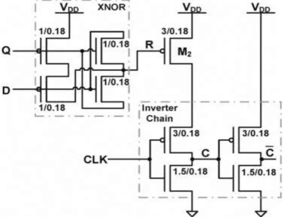
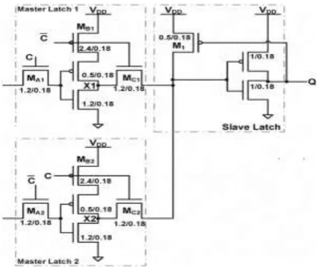
2.2 Clock Gating Circuit
The proposed DHSCGFF does not require any pulse generator; it reduces the power dissipated on the clock
network. The efficiency of the proposed DET-FF can be further enhanced by introducing a clock-gating circuit.
This simple and energy efficient clock-gating circuit is based on
Fig 2.3 Flip-Flop circuitry. Master Latch 1 is referred to as the
upper path, and Master Latch 2 is referred to as the lower path in this paper.
XNOR circuit constructed by pass transistors [8]. The pass transistor logic simplifies the circuit and reduces the
internal power dissipation.
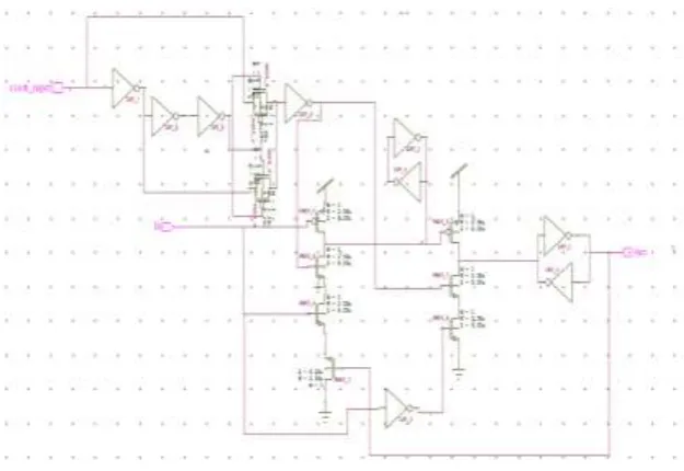
III. PROPOSED METHOD
3.1 Power Gated D Flip-Flop
The pulse generator is used which produce the dual pulse which is active at both rising and falling edge of the
clock. The C (internal gated clock) signal maintains its value instead of generating an active edge in the gating
mode. C changes after the transition on CLK in the non-gating mode.
Asynchronous data transition occurs in DET_SRSFF, when there is an input change while CLK equals 0.
Because when there is a change in the input, clock signal is made inactive. At that time when the input is stable
that means no significant change in the output. But still at that time circuit evaluate the input. This is basically
used to control the discharge path. The dual triggered pulse generator produces a brief pulse signal synchronized
331 |
P a g e
Fig 3.1 Power gated double edge triggered flip flop
Conditional precharge technique is used for removing the redundant transitions of the flip-flop to reduce the
power dissipation. The schematic of this type of circuit is shown in fig 4. In this conditional technique for
preventing the precharging of internal node discharging path is controlled when the input remains is high for
long time. The flip-flop’s output is examined and the transition is allowed only if there is a significant change in
the output of the flip-flop. The correct choice of flip-flop and its corresponding design has a deep effect in
reducing the power consumption. Pulse triggered flip-flops gave better output as compared master slave latch
flip-flops because of timing issues.
There are different types of the dual edge triggered flip-flop used in the different synchronous circuits. There are
many microprocessors which use master-slave and pulse triggered flip-flops. Master slave dual edge triggered
flip flop which is made up of two stages, one is master and other is slave. They are characterized by the positive
set up time and large D to Q delay. Also there is duplicating of the latch part one is for master and other is for
slave. Examples of master-slave flip-flops include the transmission gated transmission gated based flip-flop,
push-pull dual edge flip-flop and transmission gate latch mux (TGLM). In pulse triggered flip-flops, one is
implicit pulse triggered flip-flop in which for generating the clock pulse implicit pulse generator is used and
other one is explicit pulse triggered flip-flop in which generation of the clock pulse by explicit pulse generator.
V. EXPERIMENTAL RESULTS
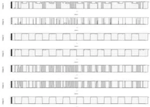
5.1 Proposed Dual Edge Triggered Flip-Flop
In this proposed circuit of flip-flop some type of controlling circuit is embedded so that clock is disabling when
the input invokes no output change. In order to eliminate the redundant transitions this data dependent technique
based flip-flop is proposed. This results in saving of the power because the clock is disable at the point when no
332 |
P a g e
5.1.1 ResultFig 5.1 Simulation Output
5.1.2 Power Results
V1 from time 0 to 2e-006
Avg power consumed -> 1.032937e-003w
Max power 4.580270e-003 at
Time 9.29607e-008
Min power 4.637432e-009 at
Time 9.3e-007
VI. CONCLUSION
Various power reduction techniques emerged as a result of high demand in mobile devices. DETFF is an
efficient technique for power reduction, when used separately. When clock gating technique is integrated
with DETFF, asynchronous data sampling problem arises at the output between two clock edges. This
problem has been defined in detail and solutions were given to eradicate it. Three simple approaches were
made to reduce the power consumed in DETFF’s by eliminating the asynchronous data sampling issue. In
order to reduce the power consumption further, a new design has been proposed and based on that, three
designs were implemented using Tanner EDA Tool.
REFERENCES
[1] M. Keating, D. Flynn, R. Aitken, A. Gibbons, and K. Shi, Low Power Methodology Manual: For
333 |
P a g e
[2] M. Pedram, “Power minimization in IC design: Principles and applications,” ACM Trans. Design Autom.
Electron. Syst. (TODAES), vol. 1, no. 1, pp. 3–56, 1996.
[3] V. Venkatachalam and M. Franz, “Power reduction techniques for microprocessor systems,” ACM
Comput. Surveys (CSUR), vol. 37, no. 3, and 2005.
[4] C.-C. Yu, “Low-power double edge-triggered flip-flop circuit design,” in Proc. Int. Conf. Innovative
Computing Information and Control (ICICIC), 2008.
[5] A. G.M. Strollo, C. Cimino, and E. Napoli, “Power dissipation in onelatch and two-latch double edge
triggered flip-flops,” in Proc. IEEE Int. Conf. Electronics, Circuits and Systems, 1999, vol. 3, pp. 1419–
1422.
[6] R. Hossain, L. Wronski, and A. Albicki, “Low power design using double edge triggered flip-flops,” IEEE
Trans. Very Large Scale Integr. (VLSI) Syst., vol. 2, no. 2, pp. 261–265, 1994.
[7] A. G. M. Strollo, E. Napoli, and C. Cimino, “Analysis of power dissipation in double edge-triggered
flip-flops,” IEEE Trans. Very Large Scale Integr. (VLSI) Syst., vol. 8, no. 5, pp. 624–629, Oct. 2000.
[8] N. Nedovic and V. G. Oklobdzija, “Dual-edge triggered storage elements and clocking strategy for low-power systems,” IEEE Trans. Very Large Scale Integr. (VLSI) Syst., vol. 13, no. 5, pp. 577–590, Oct. 2005. [9] V. Stojanovic and V. G. Oklobdzija, “Comparative analysis of master slave latches and flip-flops for
high-performance and low-power systems,” IEEE J. Solid-State Circuits, vol. 34, no. 4, pp. 536–548, Apr. 1999.
[10] K.-H. Cheng and Y.-H. Lin, “A dual-pulse-clock double edge triggered flip-flop for low voltage and high
speed application,” in Proc. IEEE Int. Symp. Circuits and Systems (ISCAS), 2003, vol. 5, pp. 425–428. [11] K. Inoue and M. Kaneko, “Variable-duty-cycle scheduling in doubleedge- triggered flip-flop-based
high-level synthesis,” in Proc. IEEE Int. Symp. Circuits and Systems (ISCAS), 2011, pp. 550–553.
[12] P. Zhao, J. McNeely, P. Golconda, M. A. Bayoumi, R. A. Barcenas, and W. K. W. Kuang, “Low-power
clock branch sharing double-edge triggered flip-flop,” IEEE Trans. Very Large Scale Integr. (VLSI) Syst.,
vol. 15, no. 3, pp. 338–345, Jun. 2007.
Biographical Notes
Ms . R . RAMYA is presently pursuing M.E. final year in Electronics & communication Engineering Department (Specialization in VLSI Design) from Hindusthan institute of technology, coimbatore, India.