Available online: https://edupediapublications.org/journals/index.php/IJR/ P a g e | 3050
Suppression of Double-Frequency Ripple with Fuzzy Control
Based Single-Phase Pv Quasi-Z-Source Inverter
Ananthu Naga Santosh & Naresh Kumar.G
1M.Tech, B V Raju Institute of Technology, Affiliated to JNTUH, Hyderabad, Telangana, India.
2Assistant Professor, B. V Raju Institute of Technology, Affiliated to JNTUH, Hyderabad, Telangana, India.
Abstract- according to the single phase photovoltaic system (PV), which exist a double frequency mismatch that exist between the dc input side and ac output side. To buffer out the double frequency ripple energy it is necessary to required. A capacitance reduction control strategy is proposed to buffer the DFR energy in single-phase Z-source/quasi-Z-source inverter applications is proposed in this paper. In single-stage photovoltaic (PV) system, there is a power irregularity exist between the AC yield and DC input. Here we are using the fuzzy logic controller, because it has many advantages comparing to other controllers. Such as, the fuzzy controller is the most suitable for the human decision-making mechanism, providing the operation of an electronic system with decisions of experts. The double-frequency ripple (DFR) energy needs to be buffered by passive network. The ripple energy will flow into the input side and adversely affect the PV energy harvest. In a conventional PV system, due to their high capacitance electrolytic capacitors are usually used. Electrolytic capacitors are considered to be one of the most failure prone components in a PV inverter. The proposed control strategy can significantly reduce the capacitance requirement and achieve low input voltage DFR. Consequently, highly reliable film capacitors can be used. Due to the proposed control strategy the increased switching device voltage stress and power loss will also be discussed. By using the simulation results we can analyze the proposed method.
Index Terms—Capacitance reduction, double-frequency ripple (DFR), Z-source (ZS)/quasi-Z-source (qZS), Fuzzy logic control.
INTRODUCTION
In the recent years for the photovoltaic application the voltage fed z-source inverter and quasi z-source inverter is considered. This inverter feature single stage buck boost transformer. It is due to shoot through capability. For the single phase and three phase applications the z-source inverter and quasi z source inverter are utilized. The voltage-fed z-source inverter (ZSI) and quasi-Z-source inverter (qZSI) has been considered for photovoltaic (PV) application in recent years [1-3]. These inverters feature single-stage buck-boost and improved reliability due to the shoot-through capability. The ZSI and qZSI are both utilized in three-phase and single-phase applications [1-5]. The single phase ZSI/qZSI can also be connected in cascaded structure
for higher voltage application and higher performance [6-10].
The mismatched ac ripple is termed as double-frequency ripple (DFR) in this paper. In three-phase applications, the Z-source (ZS)/ quasi-Z-source (qZS) network only needs to be designed to handle the high frequency ripples. However, in single-phase application, the ZS/qZS network needs to handle not only the high-frequency ripples but also the low-frequency ripple. The qZSI will be used in this paper to study the low-frequency ripple issue and present the proposed control strategy. A single-phase qZSI system is shown in Fig. 1.
Fig. 1. Diagram of a single-phase qZSI based PV system.
Ideally, the dc-side output power is pure dc and the ac-side power contains a dc component plus ac ripple component whose frequency is two times the grid voltage frequency. The mismatched ac ripple is termed as double-frequency ripple (DFR) in this paper. In order to study the low frequency ripple issues qZSI is used in this paper. A single phase qZSI system is shown in fig.1. The output power at DC side is pure DC and AC side power contains DC component plus AC ripple component whose frequency is two times the grid frequency. The mismatched AC ripple in the system is coined as double frequency ripple (DFR).
Available online: https://edupediapublications.org/journals/index.php/IJR/ P a g e | 3051
devices are applied in the inverter to increase the system efficiency at high switching frequency. Finally, experimental results are provided to verify the effectiveness of the proposed control system.
In order to balance the power mismatch between the dc side and ac side, the DFR power needs to be buffered by the passive components, mainly the qZS capacitor C1 which has higher voltage rating than C2. The DFR peak power is the same as the dc input power, so large capacitance is needed to buffer this ripple energy. To achieve high inverter power density with reasonable cost, electrolytic capacitors are usually selected.
Two additional smoothing-power circuits are employed to reduce the DFR of DC-link voltage in ZSI. However, the added circuits increase the system cost and complexity. A low-frequency harmonic elimination PWM technique is presented to minimize the double frequency ripple on Z-source capacitors. However, the method is used for application with constant voltage input source and double-frequency ripple current is induced in the inductor and the input side. This is not suitable for the PV application, because the ripple current will decrease the energy harvest from the PV panels.
PROPOSED CONTROL SYSTEM FOR CAPACITANCE REDUCATION
The basic principle of the proposed capacitance reduction method can be explained by (1).
∆𝐸 =1
2𝐶 𝑣𝐶−𝑚𝑎𝑥
2 − 𝑣
𝐶−𝑚𝑖𝑛2 (1)
where C is the capacitance, ∆E is the ripple energy that is stored in the capacitor, and vC-max and vC-min are the maximum and minimum voltages across the capacitor. According to (1), there are two ways to increase ∆E. One is to increase the capacitance C, and the other way is to increase the voltage fluctuation across the capacitor. Instead of increasing the capacitance, the proposed control system will increase the voltage fluctuation across the qZS capacitors to buffer more double-frequency power. A dedicated strategy is needed to impose the DFR on qZS capacitors while preventing the ripple energy from flowing into the input.
(a)
Fig. 2. The modulation strategy of (a) traditional method
In conventional single-phase qZSI, the modulation strategy is shown in Fig. 2(a). The two phase legs of the full bridge are modulated with 180o opposed reference waveforms, m and , m , to generate three-level voltage output. Two straight lines *p v and * vn are used to generate the shoot through duty ratio. When the triangular carrier is greater than v*p or the carrier is smaller than * vn , all four switches S1 − S4 turn on simultaneously for shoot-through.
In the proposed control system, the shoot-through control lines * v p and vn* are modified to a line with doublefrequency component as shown in Fig. 2(b).
(b)
Fig. 2. The modulation strategy of (b) proposed method.
By doing so, the dc side and the qZS capacitor DFR can be decoupled. An input DFR suppression controller is added in the control system to generate the double-frequency component in v*p and * vn .
Available online: https://edupediapublications.org/journals/index.php/IJR/ P a g e | 3052
and its output is the magnitude of the grid current reference. The grid current ig is regulated by controlling the inverter modulation index m through a proportional resonant (PR) controller. The PR controller has a resonance frequency equal to the grid frequency. The qZS capacitor voltage is regulated by controlling dSH. If the inverter loss is not enough to damp the oscillation, dedicated active damping is needed to deal with the oscillation and vC2 information is required for the implementation. Due to the limited space, the detail of the active damping is not presented in this paper and will be covered in future paper. The vC2 voltage controller only regulates the average value of vC2, which is Vc2_ave, due to the low-pass filter in the signal feedback with a cutoff frequency of 25Hz. Therefore, the capacitor voltage controller has limited influence on double frequency component and most DFR
energy can be kept in qZS capacitors. Vdc_ave* should be selected carefully so that the value of dSH does not become negative because of the double-frequency swing, and the summation of dSH and m is always smaller than 1. A feed forward component Vc2*/ Vdc_ave* is added to the output of the capacitor voltage controller to increase the dynamic performance.
IMPACT OF CAPACTICANCE REDUCTION A. System stability
In order to apply the proposed control system, it is necessary to study impact of decreasing C1 on system stability. The possible operation states of voltage fed qZSI have been presented in [13] and it is summarized in the appendix with equivalent circuits, and the averaged model of qZSI can be obtained as in (2).
𝐿1 𝑑𝑖𝐿1
𝑑𝑡 = 1 +
𝑇𝐴𝐵+𝑇0𝐵
𝑇𝑠−𝑇𝐴𝐵−𝑇0𝐵 𝑣𝐶1+ 𝑣𝐶2 𝑑𝑆𝐻+
𝑇𝑆𝐵𝑈
𝑇𝑠−𝑇𝐴𝐵−𝑇0𝐵 𝑣𝐶1+ 𝑣𝐶2 − 𝑣𝐶1+ 𝑣1𝑁 𝐿2𝑑𝑖𝐿2
𝑑𝑡 = 1 +
𝑇𝐴𝐵+𝑇0𝐵
𝑇𝑠−𝑇𝐴𝐵−𝑇0𝐵 𝑣𝐶1+ 𝑣𝐶2 𝑑𝑆𝐻+
𝑇𝑆𝐵𝑈
𝑇𝑠−𝑇𝐴𝐵−𝑇0𝐵 𝑣𝐶1+ 𝑣𝐶2 − 𝑣𝐶2 𝐶1
𝑑𝑣𝐶1
𝑑𝑡 = 𝑖𝐿1− 𝑖𝐿1+ 𝑖𝐿2 𝑑𝑆𝐻− 𝑇𝑆𝐵𝑈
𝑇𝑠 𝑖𝐿1+ 𝑖𝐿2 −
𝑇𝐴𝐶
𝑇𝑠 +
𝑇𝐴𝐵
𝑇𝑠 𝑖𝐷𝐶 𝐶2𝑑𝑣𝑑𝑡𝐶2= 𝑖𝐿2− 𝑖𝐿1+ 𝑖𝐿2 𝑑𝑆𝐻−𝑇𝑆𝐵𝑈𝑇
𝑠 𝑖𝐿1+ 𝑖𝐿2 −
𝑇𝐴𝐶
𝑇𝑠 +
𝑇𝐴𝐵
𝑇𝑠 𝑖𝐷𝐶
(2)
where T s is the switching period, TAB, T0B, TSBU, TAC, and TSBI are time intervals of different operation states, as listed in the appendix, m is the modulation signal and dSH = TSBI / Ts. The small signal model can be derived accordingly as in (3).
𝐿1 𝑑𝑖 𝐿1
𝑑𝑡 = 1 +
𝑇𝐴𝐵+𝑇0𝐵
𝑇𝑠−𝑇𝐴𝐵−𝑇0𝐵 𝑣𝐶1+ 𝑣𝐶2 𝑑 𝑆𝐻+
𝑇𝑆𝐵𝑈
𝑇𝑠−𝑇𝐴𝐵−𝑇0𝐵 𝑣 𝐶1+ 𝑣 𝐶2 − 1 − 𝐷𝑠 𝑣 𝐶1+ 𝐷𝑠𝑣 𝐶2+ 𝑣1𝑁 𝐿2
𝑑𝑖𝐿2
𝑑𝑡 = 1 +
𝑇𝐴𝐵+𝑇0𝐵
𝑇𝑠−𝑇𝐴𝐵−𝑇0𝐵 𝑣𝐶1+ 𝑣𝐶2 𝑑𝑆𝐻+
𝑇𝑆𝐵𝑈+𝑇𝐴𝐵+𝑇0𝐵
𝑇𝑠−𝑇𝐴𝐵−𝑇0𝐵 𝑣 𝐶1+ 𝑣 𝐶2 − 1 − 𝐷𝑠 𝑣 𝐶2+ 𝐷𝑠𝑣 𝐶1 𝐶1𝑑𝑣 𝑑𝑡𝐶1= 1 − 𝐷𝑆−𝑇𝑆𝐵𝑈𝑇
𝑠 𝑖 𝐿1− 𝐷𝑆+
𝑇𝑆𝐵𝑈
𝑇𝑠 𝑖 𝐿2+ 𝐼𝑙1+ 𝐼𝑙2 𝑑 𝑆𝐻−
𝑇𝐴𝐶
𝑇𝑠 +
𝑇𝐴𝐵
𝑇𝑠 𝑖 𝐷𝐶 𝐶1𝑑𝑣 𝐶1
𝑑𝑡 = 1 − 𝐷𝑆−
𝑇𝑆𝐵𝑈
𝑇𝑠 𝑖 𝐿1− 𝐷𝑆+
𝑇𝑆𝐵𝑈
𝑇𝑠 𝑖 𝐿2+ 𝐼𝑙1+ 𝐼𝑙2 𝑑 𝑆𝐻−
𝑇𝐴𝐶
𝑇𝑠 +
𝑇𝐴𝐵
𝑇𝑠 𝑖 𝐷𝐶
(3)
This RHP zero will limit the system dynamic response. However, the decrease of C1 will not significantly change the position of the RHP zero. There are two pairs of conjugated poles located on the imaginary axis, which indicate possible resonances at two different frequencies. The lower-frequency resonance is more related to C1 and the higher-frequency resonance is mainly determined by C2. Therefore, it is seen that the higher resonant frequency does not change much with the C1 change. The lower resonant frequency increases when C1 decreases. Because there is always a zero close to the lower-frequency pole, the lower-frequency resonance is largely damped. Decreasing C1 does not affect the system stability much.
Fig. 4. Root loci of the system with C1 parameter sweeping.
Available online: https://edupediapublications.org/journals/index.php/IJR/ P a g e | 3053
When the proposed method is applied, the doublefrequency voltage ripple across vC1 and vC2 will be increased intentionally. The dc link voltage across the H-bridge vDC will also include DFR which could increase the voltage stress of switching devices. Because vC1 is much higher than vC2, most double-frequency energy is stored in C1. The value of vC1 can be calculated using the following equation
1 2𝐶1𝑣𝐶1
2 =1
2𝐶1𝑣𝐶1−𝑎𝑣𝑒
2 + 𝑃
𝑖𝑛− 𝑃𝐴𝐶 𝑑𝑡 𝑡
0 (4)
where V ave c1 _ is the average value of vC1, Pin is the input power and pAC is the instantaneous ac output power. pAC can be calculated in (6).
𝑃𝐴𝐶 = 𝑉𝑔−𝑝sin 𝜔𝑡 ∗ 𝐼𝑔−𝑝sin 𝜔𝑡 =
12𝑉𝑔−𝑝𝐼𝑔−𝑝1−𝑐𝑜𝑠2𝜔𝑡=𝑃𝑖𝑛1−𝑐𝑜𝑠2𝜔𝑡(5)
where V g_p and Ig_p are the peak value of vg and ig. Therefore, we can get
𝑣𝐶1= 𝑣𝐶1−𝑎𝑣𝑒 + ∆𝑣𝐶1−𝑑𝑓𝑟 =
𝑉𝑐1−𝑎𝑣𝑒2 + 𝑃𝑖𝑛
𝜔 𝐶1sin 2𝜔𝑡 =
𝑉𝑑𝑐 −𝑎𝑣𝑒+𝑉𝑖𝑛
2 2
+𝑃𝑖𝑛
𝜔 𝐶1sin 2𝜔𝑡 (6)
where ∆vc _1 dfr is the DFR component of vC1. In (7), the value of Vin and Pin are determined by the PV array operating point. Vdc_ave is indirectly controlled by regulating Vc2_ave as shown in Fig.3. Therefore, when Vdc_ave* is selected and the PV array operating point is determined, vC1 can be calculated. It is seen that larger ∆vc _1 dfr can reduce the size of C1. vDC during non-shoot period can be obtained as
𝑣𝐷𝐶= 2𝑣𝐶1− 𝑣𝑖𝑛
= 2 𝑉𝑑𝑐 −𝑎𝑣𝑒+𝑉𝑖𝑛
2 2
+𝑃𝑖𝑛
𝜔 𝐶1sin 2𝜔𝑡 − 𝑉𝑖𝑛 (7)
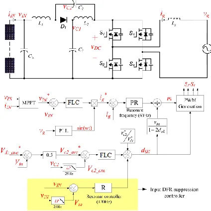
It is seen from (8), when C1 and Pin are fixed, the switching device voltage stress is mainly determined by Vdc_ave and Vin. There is an optimized value of Vdc_ave* for different input voltage conditions to minimize the switching device voltage stress.
𝑚 =𝑉𝑔−𝑝sin 𝜔𝑡
𝑣𝐷𝐶 (8)
In order to take advantage of the buck-boost feature of the qZSI, the input voltage range is usually selected that Vg_p is among the input voltage range. For the proposed method, the maximum switching device voltage stress could happen at maximum or minimum Vin. When Vin is larger than Vg_p, no shoot-through is needed in conventional design and dSH equal to zero. However, for the proposed method, certain value of D sh_ave is needed to make sure dSH does not become negative values because
of the double-frequency swing. Higher Vin leads to higher peak value of vDC. Therefore, one of the worst cases for the increased device voltage stress could happen at maximum Vin.
Fig. 5. V∗dc-ave and switching device voltage stress at different input voltages.
FUZZY LOGIC CONTROLLER
In FLC, basic control action is determined by a set of linguistic rules. These rules are determined by the system. Since the numerical variables are converted into linguistic variables, mathematical modeling of the system is not required in FC.
Fig.6.Fuzzy logic controller
The FLC comprises of three parts: fuzzification, interference engine and defuzzification. The FC is characterized as i. seven fuzzy sets for each input and output. ii. Triangular membership functions for simplicity. iii. Fuzzification using continuous universe of discourse. iv. Implication using Mamdani‟s, „min‟ operator. v. Defuzzification using the height method.
TABLE I: Fuzzy Rules
Available online: https://edupediapublications.org/journals/index.php/IJR/ P a g e | 3054
to appropriate system. The value of input error and change in error are normalized by an input scaling factor.In this system the input scaling factor has been designed such that input values are between -1 and +1. The triangular shape of the membership function of this arrangement presumes that for any particular E(k) input there is only one dominant fuzzy subset. The input error for the FLC is given as
E(k) = Pp h (k )−Pp h (k −1)
Vp h (k )−Vp h (k −1) (9)
CE(k) = E(k) – E(k-1) (10)
Inference Method: Several composition methods such as Max–Min and Max-Dot have been proposed in the literature. In this paper Min method is used. The output membership function of each rule is given by the minimum operator and maximum operator. Table 1 shows rule base of the FLC.
Defuzzification: As a plant usually requires a non-fuzzy value of control, a defuzzification stage is needed. To compute the output of the FLC, „height‟ method is used and the FLC output modifies the control output. Further, the output of FLC controls the switch in the inverter. To achieve this, the membership functions of FC are: error, change in error and output
The set of FC rules are derived from
u=-[α E + (1-α)*C] (11)
Fig 7 input error as membership functions
Fig 8 change as error membership functions
Fig.9 output variable Membership functions Where α is self-adjustable factor which can regulate the whole operation. E is the error of the system, C is the change in error and u is the control variable.
SIMULATION RESULTS
For the proposed method, there is a design trade-off between the demand of decreasing C1 and the increased voltage stress across the switching devices.
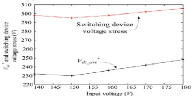
Fig.10 Block diagram of simulation TABLE II.
Parameters Of The Qzsi Under Study
They are provided in Fig. 10. It is seen that the maximum voltage stress across the switching devices happens at Vin=180V in this design.
Fig. 11. The vDC, vIN and vC2 waveforms of the qZSI with the conventional control, C1=2mF.
Fig. 12. The vDC, vIN and vC2 waveforms of the qZSI with the conventional control, C1=200µF
Available online: https://edupediapublications.org/journals/index.php/IJR/ P a g e | 3055
Fig. 13. The vDC, vIN and vC2 waveforms of the qZSI with the proposed control, C1=200µF.
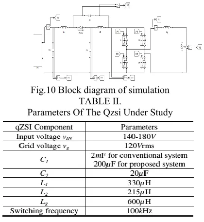
The efficiency comparison of the conventional qZSI and the qZSI with proposed control at different power outputs is provided in Table. III.
TABLE III.
Efficiency Comparison Of The Conventional Qzsi And Qzsi With The Proposed Control
Fig. 14. The output current waveform of the qZSI with the proposed control, C1=200µF.
CONCLUSION
According to the new control strategy is proposed to minimize the capacitance requirement in single-phase qZSI PV system. The proposed control system incorporates a modified modulation strategy and a DFR suppression controller. Instead of using large capacitance, the qZS capacitors are imposed with higher double-frequency voltages to store the double-frequency ripple energy. In FLC, basic control action is determined by a set of linguistic rules. These rules are determined by the system. The FLC comprises of three parts: fuzzification, interference engine and defuzzification. By using the fuzzy controller for a nonlinear system allows for a reduction of uncertain effects in the system control
and improve the efficiency. In order to prevent the ripple energy flowing into the input PV side, a modified modulation and an input DFR suppression controller are used to decouple the input voltage ripple from the qZS capacitor DFR. The small signal model is developed and shows that the capacitance reduction does not impact the system stability.In this paper capacitance reduction control strategy is proposed to buffer the DFR energy in Z source or Quasi Z source inverter application. The proposed control strategy can significantly reduced the capacitance requirement without using any extra hardware component. This can also achieve low input voltage DFR. Consequently a highly reliable film capacitors can used.
REFERENCES
[1] Y. Li, S. Jiang, J.G. Cintron-Rivera, and F. Z. Peng, “Modeling and Control of Quasi-Z-Source Inverter for Distributed Generation Applications,” IEEE Trans. Ind. Electron., vol.60, no.4, pp. 1532- 1541, Apr. 2013.
[2] Y. Huang, M. Shen, F.Z. Peng, and J. Wang, “Z -Source Inverter for Residential Photovoltaic Systems,” IEEE Trans. Power Electron., vol.21, no.6, pp. 1776-1782, Nov. 2006.
[3] D. Cao, S. Jiang, X. Yu, and F. Z. Peng, “Low-Cost Semi-Z-source Inverter for Single-Phase Photovoltaic Systems,” IEEE Trans. Power Electron., vol.26, no.12, pp.3514-3523, Dec. 2011. [4] W. Wei, H. Liu, J. Zhang and D. Xu, “Analysis of power losses in Zsource PV grid-connected inverter,” in Proc. IEEE 8th International Conference on Power Electronics and ECCE Asia (ICPE & ECCE), May 30-Jun. 3, 2011, pp. 2588-2592.
[5] T.W. Chun, H.H. Lee, H.G. Kim, and E.C. Nho, “Power control for a PV generation system using a single-phase grid-connected quasi Z source inverter,” in Proc. IEEE 8th International Conference on Power Electronics and ECCE Asia (ICPE & ECCE), May 30-Jun. 3, 2011, pp. 889-893.
[6] L. Liu, H. Li, Y. Zhao, X. He, and Z. J. Shen, “1 MHz cascaded Zsource inverters for scalable grid-interactive photovoltaic (PV) applications using GaN device,” in Proc. IEEE Energy Convers. Congr. Expo., Sep. 17-22, 2011, pp. 2738–2745.
[7] B. Ge, Q. Lei, F. Z. Peng, D. Song, Y. Liu, and A.R. Haitham, “An effective PV power generation control system using quasi-Z source inverter with battery,” in Proc. IEEE Energy Convers. Congr. Expo., Sept. 17-22, 2011, pp.1044-1050.
Available online: https://edupediapublications.org/journals/index.php/IJR/ P a g e | 3056
using eGaN FETs,” IEEE Trans. Power Electron., vol. 28, no. 6, pp. 2727–2738, Jun. 2013.
[9] Y. Zhou and H. Li, "Analysis and Suppression of Leakage Current in Cascaded-Multilevel-Inverter-Based PV Systems," IEEE Trans. Power Electron., vol.29, no.10, pp.5265-5277, Oct. 2014.
[10] L. Liu, H. Li, Y. Xue and W. Liu, “Decoupled Active and Reactive Power Control for Large-Scale Grid-Connected Photovoltaic Systems Using Cascaded Modular Multilevel Converters,” IEEE Trans. Power Electron., vol.30, no.1, pp.176-187, Jan. 2015.
[11] D. Sun, B. Ge, F. Z. Peng, A. R. Haitham, D. Bi, and Y. Liu, “A new grid-connected PV system based on cascaded H-bridge quasi-Z source inverter,” in Proc. IEEE Int. Symp. Ind. Electron., May 28–31, 2012, pp. 951–956.
ANANTHU NAGA SANTOSH
Completed B.Tech in Electrical & Electronics Engineering in 2015 from Malla Reddy Institute of Engineering and Technology, Affiliated to JNTU UNIVERSITY, HYDERABAD and Pursuing M.Tech form B V Raju Institute of Technology, Affiliated to JNTUH, Hyderabad, Telangana, India. Area of interest includes Energy systems.
E-mail id: [email protected]
NARESH KUMAR.G
Completed B.Tech in Electrical & Electronics Engineering in 2008 from JNTU, Hyderabad and M.Tech in Energy Systems JNTU Anantapur in 2010, working as Assistant Professor at BVRIT, Narsapur with an experience of 7 years. Area of interest – Renewable Energy Sources and Power Quality.