FPGA implementation of Reconfigurable Analog Modulation
Schemes on Software Defined Radio
KurraSeva Naik& Sanjay Dubey
M.Tech VLSI System Design B.V. Raju Institute of Technology(autonomous), Narsapur,Medak,Telangana,India.
Mr.Prof.SanjayDubey Department of ECE B.V. Raju Institute of Technology(autonomous), Narsapur,Medak,Telangana,India.
Abstract: This project aims to RTL designing and FPGA implementation of the two different Waveforms (Amplitude, Frequency modulations and demodulations) and reconfiguring them on a software defined radio. Waveforms will sit in the external BPI NOR flash memory and reconfiguring them dynamically to change their structure and functionality in order to better suit the task at hand and to increase the capabilities of FPGAs slice. Multi boot methodology is adopted to perform the goal of the work.
Key words: FPGA, RTL design, AM and FM, JTAG, SDR, BPI flash memory, Multi boot methodology.
INTRODUCTION:
Software defined radio is an
intelligent radio that can be programmed and configured dynamically from the front panel
side, then accordingly changes
its transmission or reception parameters
(waveforms, operating frequency) to allow more concurrent wireless communications in a given spectrum band at one location.
Multi boot describes the process by which the FPGA selectively reprograms and reloads its bit stream from an attached external memory. Multi boot feature allows, the FPGA application to load two or more FPGA bit streams under the control of FPGA application. One of the most interesting features of reconfigurable systems is their ability to
dynamically change their structure and functionality in order to better suit the task at hand. For FPGAs, those changes to structure and functionality are made by loading configuration bit stream data through one of several configuration ports.
External configuration ports such as the Select MAP and JTAG interfaces are typically driven by an external device such as a PC. In contrast, the internal configuration access port (ICAP) can be directly accessed by application circuits configured on the FPGA, allowing them to change their own structures and functionalities at run time. To achieve this, different RTL design with different
Functionalities are loaded onto the FPGA when needed by those applications.
1.1Need for the Project
Voice communication is a fast growing area in communication and networking. In order to increase the versatility and flexibility of communication requirements of today's fluid air and land warfare, there is a need for a multi-functional radio set that will be able to perform multiple roles and work in different modes. In order to derive maximum benefit from the latest advancements and also to avoid equipment being outmoded soon after production, it is possible to design/procure equipment on this
Qualitative Requirement (QR), The
entire radio sets of the Indian Army and Air Force to SDR
1.2Objective of the Project
FPGA Implementation of the two different modulation and demodulation schemes such as Amplitude and Frequency modulation schemes. Both the configurations (AM and FM) will sit in the external BPI NOR flash memory and reconfiguring them dynamically to change their structure and functionality and since both the processor and FPGA works with different clock frequencies so to avoid clock domain crossing, Developed a GPMC interface between the processor and FPGA for synchronous communication.
1.3Used Hardware Platform
FPGA: kintex-7 325t-1ffg676. Processor: TMS320DM8148
Language used: Verilog Hardware Description language.
1.4 Design Entry
There are different techniques for design entry. Schematic based, Hardware Description Language and combination of both etc. Selection of a method depends on the design and designer. If the designer wants to deal more with Hardware, then Schematic entry is the better choice. When the design is complex or the designer thinks the design in an algorithmic way then HDL is the better choice. Language based entry is faster but lag in performance and density.
1.5 Synthesis
The process which translates VHDL or Verilog code into a device netlist format.i.e a complete circuit with logical elements (gates, flip flop, etc…) for the design. If the design contains more than one sub designs, ex. to
implement a processor, we need a CPU as one design element and RAM as another and so on, then the synthesis process generates net list for each design element.
2. FPGA configuration interfaces:
Several external interfaces and an internal interface accessible to the user exist for the purpose of configuring the FPGA. However, all these interfaces internally use the same serial configuration interface of the FPGA. The JTAG interface is dedicated and has preference over all other interfaces. The other interfaces are multiplexed and share the same I/O banks.
2.1 The JTAG interface:
The external four-pin JTAG interface implements the IEEE 1149.1 standard, defining the Test Access Port (TAP) and Boundary-Scan Architecture. This standard ensures the board-level integrity of individual components and the interconnections between them. Additionally, Boundary-scan architecture offers the flexibility for vendor-specific instructions, such as configure and verify, which add the capability to load configuration data directly to FPGAs and readback configuration. The Test Access Port and boundary-scan architecture is commonly referred to as JTAG. The mode settings for the JTAG interface are 101.
2.2Internal Configuration Access Port:
enable and the RDWRB input port is to select
the ICAPE2 operation, i.e. device
reconfiguration or configuration read back. Earlier versions of the ICAP interface also have a BUSY output signal for signaling status during reconfiguration. This was removed in the latest version of the interface. The configuration status is sent back through the output port. During system run-time, a master device, usually an embedded processor can transfer the partial reconfiguration bit stream from the configuration memory to the ICAP interface to perform the reconfiguration process.
2.3A brief history of AM and FM
The history of radio broadcasting started in the beginning of the 20th century with the introduction of the Amplitude Modulation (AM) system in which the amplitude of the carrier is modulated by the amplitude of the message signal as demonstrated. Albeit relatively simple in both theory and practice, AM suffers more from additive noise than FM does.
3. Project Development
Software defined radio is an enabling technology, applicable across a wide range of areas within the wireless industry, that provides an efficient and comparatively inexpensive solutions to several of the problems inherent in more traditional radio architectures. It is important that a SDR be able to process many different waveforms for it to be viable. This includes legacy “analog” waveforms such as Analog modulation (AM) and frequency modulation (FM). This work reconfigures the two different waveforms AM and FM schemes in the SDR, when the target platform is a field-programmable gate array (FPGA). FPGAs are often included as an integral part of SDRs because they handle digital signal processing (DSP) algorithms very well. FPGAs are also reconfigurable.
3.1Design Description:
The input audio was voice from microphone/handset is given to the codec. At application level audio data was read / Write using ALSA driver from codec. GPMC driver (PROCESSOR) collects the samples and fed to the FPGA where the AM/FM modulation was carried out for the received voice packets and the digital modulated output from the modulator module was fed to the Analog interfacing called DAC.
In GPMC driver (Processor) input data is given to the FPGA which needs to be modulated and when the data is requested by application, GPMC driver waits for interrupt from the FPGA and read the demodulated data from FPGA and given it to the application.
GPMC interface in the FPGA collects data samples from the GPMC driver (processor) and writes into write buffer/FIFO at GPMC clock of 100 MHz
At the Transmitter chain the FPGA reads this data from Write FIFO at 8KHz FPGA clock and sent to the interpolator block. The 8Ksps 16 bit data is up-converted to 125 MSPS using Interpolator and fed to the modulator module. The output of modulator module is of 16 bit 125Msps signal at 21.4MHz IF. This digital modulated signal is converted to Analog form using DAC of 125MSPS and is given to RF front end receiver.
Similarly at the Receiver chain, The ADC input signal which is 21.4MHz IF from RF front end transmitter was read by the FPGA and sent to the Demodulator block, thereby the down sampled digital demodulated data of 8ksps is sent to read buffer/FIFO at FPGA clock of 8KHz. The GPMC will receive this signal and demodulated output is given to codec to listen at headset/handset.
4. PROGRAMMING THE HARDWARE
The Programming of FPGA is done using JTAG and programming has four steps
1. Identify the device by selecting boundary scan chain.
2. Initialize JTAG chain.
3. Assign New Configuration File. Program the device.
4.2Programming of FPGA with the available attached BPI flash connected
Step1: Identify the device by selecting boundary scan chain
After the successful generation of the MCS file double click the boundary scan option available at the left panel in Impact window then right click to add device file or initialize JTAG chain figures are shown after that select the specified device in the device properties window.
Step2: Add the BPI flash:
Right click on the Add SPI/BPI flash shown in the window then add the PROM file to beloaded in the flash.
Step 3: Select Numonyx 28F512P30 Device Part Number
After selecting the BPI PROM file to load, iMPACT displays the Select Attached SPI/BPI
dialog box (Figure4.8) the third step of the process requires the target BPI PROM type to be specified in this dialog box. Select the BPI PROM type. Then select the Numonyx 28F512P30 part number for the target BPI PROM used in this demonstration, and select the Data Width and RS [1:0] b Pin Address Bits selections as 16 and [25:24]. Click OK to complete the BPI PROM programming setup.
Step 4: Set Device Programming Properties
The fourth step sets the programming properties for the BPI flash device attached to the Kintex-7 FPGA. In the category window of the Device Programming Properties dialog box, select Device (Attached FLASH, 28F512P30). Ensure that the Verify and Erase
before Programming properties are checked. Click OK to continue to step 5.
Step 5: Invoke the iMPACT Program Operation
The fifth step of the process programs the target BPI PROM with the selected BPI PROM file contents. Ensure the BPI PROM icon in the iMPACT window is selected by left-clicking on the BPI PROM icon (the BPI PROM icon is highlighted in green when selected). Select
Operations and then Program to begin programming
5. Results and Discussions
5.1RTL Schematics of GPMC Interface for the AM/FM designs
(a) RTL Schematic of GPMC interface for the AM design and (b) FM design.
The figure represents the RTL Schematic of GPMC Interface generated by the Xilinx ISE tool. GPMC interface was the Top module where integration of all the modules were done under it. It Figures out the connections between the individual modules. In order to trigger multi-boot event Reconfiguration module should be integrated in all the Revisions or Configurations where user needs to configure.
5.2Reconfiguration Module Verification:
1. Case Name :
Reconfiguration_module_test.v
2. Test case Test Objective:
Test objective is to send 32 bit command sequence to the ICAP used to access the configuration memory, based on the trigger input selection provided from the processor.
3. Compile and Run the Test case in simulation
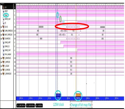
Figure 5.2 Reconfiguration module Processing.
The red color circle present on the image indicates that the 32 bit command sequence sent to the ICAP only when the Trigger input is set to the reconfiguration module.
Once the completion of sending the command sequence, the configuration memory of the FPGA will be reset and change of bit map file will be happened which will be taken from the address set in the WBSTAR register.
5.3Dynamic Reconfiguration of AM and FM on Software Defined Radio (SDR)
In general, if you need to change the configuration of the FPGA, you need to switch off the board supply and again you need to download the new configuration by using external configuration interface like JTAG. Here it’s not the case. Dynamically changing the configurations (In our case AM and FM) by manually controlling the rotary switch from the front panel of the radio shown in the figures below.
After switching on the radio, the radio will boot the initial configuration (AM) from the Flash memory.
Whenever user wish change of application, by rotating the Rotary switch at the front panel
of the radio it can be triggered to the respective bit file or configuration taken from the Flash memory.
FM is the second configuration present in the Byte peripheral Interface (BPI) Flash memory; it was under the user control whenever user needs it can be put into the FPGA.
5.4Resource utilization:
5.4.1 Available FPGA resources
Slices Flip- flops
LUTs DSP48E1s Block- RAMS
407600 3,440 203,800 840 445
5.4.2 Complete design
Slic es
Fli p-flo ps
LU Ts
DSP48E 1s
Bloc k-RA MS
Amount used
405 5
215 7
280 6
138 4
Percenta ge ofavaila ble resource s
1% 62
%
1% 16% 1%
Table 5.3 summarizes the area usage for the complete AM design Top module and percentage of available resources.
6. Conclusions and Future Scope
6.1 Conclusions
1.The development of Modulator, Demodulator and Reconfiguration modules has been done in
RTL domain using Verilog Hardware
Description language
2. After development was done, performed behavioral check syntax using Xilinx ISE.
The code written in Hardware description Language was thoroughly verified using Xilinx ISE ISIM. Since functional verification has become one of the most challenging areas in chip design.
3.The design has been synthesized successfully using XST (Xilinx synthesis Technology) Xilinx ISE tool
4.Successfully generated device programming Bit map (.bit) file in order to program the FPGA and has been tested successfully over the hardware and corresponding steps has been presented above. During implementation there occurred some timing errors but they are resolved.
5.MCS file creation also done successfully using Xilinx iMPACT tool to load the MCS file in the BPI FLASH memory.
5.Implementation has been done on SDR board and the targeted FPGA was Kintex-7 series.
Using this SDR board, AM and FM audio signals were successfully modulated and demodulated and fed to a handset/ headset. Behavioral model simulation was also undertaken before loading the bit file into FPGA.
This design is not too large to fill a modern FPGA, So additional processing can be performed on the same device if desired. Summarizing, SDR is a promising technology that facilitates development of multi-feature, multi-band, multi-service consumer handsets.
6.2 Future Scope
To improve the performance of the current work in future extensions, Multi-mode of SDR can be extended to work Voice, Data and Video communications. More revisions will be based on the revision selection (RS) pins available for the FPGA. In this thesis SDR has limited to work for voice communication i.e, AM/FM legacy waveforms. The development of SDR would enable migration of entire radio sets of the Indian Army and Air Force to SDR eventually culminating in a Cognitive Radio yet another field in which a lot of research is in progress all round the world.
REFERENCES:
[1] I. Hatai, I. Chakrabarti,
FPGAimplementation of a digital FM modem
for SDR architecture. IEEE conference on Computers and devices
for communications. January 2009.
[2] “7 Series FPGAs Configuration User Guide”, Xilinx user guide UG470 V1.10, May 2015. [3]Lai, V and Diessel, O. “ICAP-I: A reusable
interface for the internal reconfiguration of Xilinx
FPGAs,” IEEE International Conference on Field-Programmable Technology, 2009. FPT 2009, Dec 2009
[4] Dr. Hikmat N. Abdullah, B.Sc. Hussein A. Hadi, ”Design and Implementation of FPGA based Software Defined Radio Using Simulink HDL Coder“ CUAS Journal.
[5] Samir Palnitkar, Verilog HDL A guide to Digital Design and Synthesis, SunSoft Press 1996.
[7] C. Claus, F. H. Muller, J. Zeppenfeld& W. Stechele. A new framework to accelerate
Virtex-II Pro dynamic partial
selfreconfiguration. Parallel and Distributed Processing Symposium. March 2007, pp. 1 - 7. [8] “DDS compiler 2.1 datasheet”, Xilinx logicore, DS558 March 24, 2008
[9] Yuh-Ren Tsai and Xiu-Sheng Li, “Kasami Code-Shift-Keying Modulation for Ultra Wideban- d Communication Systems”, IEEE Transactions on Communications, Vol. 55, No. 6, PP. 1242-1252, June 2007
About Author
KURRA SEVA NAIK
Department: M.Tech VLSI System Design