Multifunctional DVR with Simple Inverter
Scheme Using Voltage and Current Control
Dony John1, Surumi Hassainar2
PG Student [PEPS], Dept. of EEE, FISAT Engineering College, Angamaly, Kerala, India1
Assistant Professor, Dept. of EEE, FISAT Engineering College, Angamaly, Kerala, India2
ABSTRACT: Multifunctional Dynamic voltage restorer (DVR) is a power electronic converter based custom power device used to compensate for voltage variations and to limit the fault current. This study proposes a new scheme for multifunctional DVR based on a simple inverter scheme and a different control scheme. In the proposed DVR, a ac-dc converter is attached to the grid. The dc-link voltage is regulated by a different control scheme including voltage and current control. This results in better quality of output voltage in both deep and shallow voltage sags. It is important to emphasis that the existing inverter-based DVR topologies do not have the capability of third harmonic elimination, Consistency in DC link voltage, Better output for inverter section, efficient modulation scheme incorporation etc. The system model is carried out in MATLAB/SIMULINK environment. With the aids of the proportional-integral controllers, dq0-abc transformation Level shifted pulse-width modulation control technique; the inverter control system is managed. Phase lock loop (PLL) is used to lock grid frequency and phase. The design of low pass filter used at the inverter output to remove the high frequency ripple is also discussed and the obtained simulation results are presented.
KEYWORDS: Dynamic voltage Restorer, Fault current limiter, Voltage and current control, stationary frame
I.INTRODUCTION
With the rapid development of modern electrical power industry and the great changes of electrical load in system, more users use the new equipments with good performance and high efficiency, but these equipments are sensitive to the changes of system voltage. Voltage sag is such a crucial problem that the modern power system mainly deals with which introduce enormous loss in the system. The dynamic voltage restorer (DVR) which has appeared in recent years is another important member of the flexible AC transmission systems (FACTS).
DVR is connected in series between the system voltage and the sensitive load to compensate voltage sag of sensitive load caused by system voltage sag. Voltage sags are generally related with system faults but can also be caused by the energization of heavy loads or starting of large motors loose connection in wiring and Load transferring from one power source to another. Now, Short Circuit faults remain one of the most common faults in the grid and causes great concern for grid security and stability. So in order to eliminate those two vital problems Multifunctional DVR with Inverter is introducing to the power system. The system acquires DC link voltage stability with a different control scheme.
II.PROPOSED FCL-DVRCONCEPT
For many power systems, it would be tremendously advantageous to provide both voltage compensation and fault current limiting functions by a single power electronic apparatus. In the control strategy of a conventional DVR is expanded to offer additional fault current interruption features. However, this approach requires a three-fold increase in power rating of the DVR, leading increase in system cost.
Here a concept of fault current limiting dynamic voltage restorer (FCL-DVR) with a new control scheme is proposed. The new topology can operate in two operational modes:
compensation mode for voltage fluctuation and unbalance
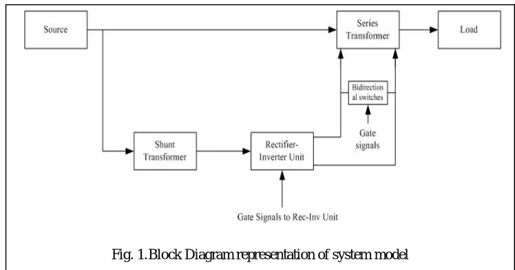
same power rating as the conventional DVR without FCL function. The block diagram representation of the system is as shown below:
III.VOLTAGE COMPENSAT ION AND FAULT CURRENT LIMITING MODE
In the proposed mode of operation system has three main switching strategy 1.Grid is in Normal mode (No compensation required)
2.PCC voltage unbalance is their but no fault – FCL DVR operates in voltage compensation mode and the bidirectional switch is not activated.
3.Any fault occur – The healthy phase of FCL-DVR operate in voltage compensation mode and bidirectional switches corresponding to the faulted phase is activated. Thus the fault current is limited through the faulted path. Then it will return to the voltage compensation mode after the fault condition is removed.
IV.CIRCUIT DIAGRAM REPRESENTATION
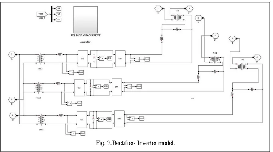
The topology of the FCL-DVR in matlab model is as shown in figure(2). It is composed of three single phase bridges. Each single phase topology mainly comprises of a shunt transformer, a back to back power converter, a series transformer, and a bidirectional switch. The input rectifier module of the back to back converter is connected to the grid through a shunt transformer with Lz to eliminate the high frequency ripples, and rectifies the power from the grid to the dc link capacitor. The output inverter module converts the power from the dc link capacitor to compensate voltage fluctuation, and is connected to the grid through a series transformer T4 and a LC output filter. The input rectifier module and output inverter module are connected through the dc link capacitor Cd. The bidirectional switch in each phase is across the output terminals of the output inverter module to provide short circuit fault current limiting function.
Us, Udc, Uc, Ud, and Ul represent the supply voltage, the dc link voltage, the output voltage of the FCL-DVR, the output
voltage of FCL-DVR on the primary side of the series transformer, and the voltage of point of common coupling (PCC), respectively. Is represents the supply current, and Il is the load current. Zs and Zl are the equivalent impedances
of the grid and the transmission line, respectively. In the system the rating of the injection transformer is same as that of compensation voltage required. Thus the three fold power rating is minimized. With voltage and current control more stabilization in DC link voltage is achieved to around 800V.
V.PRINCIPLE OF OPERATION
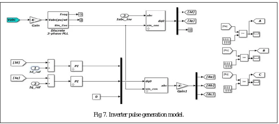
When system is working in voltage compensation mode the bidirectional switches across each output phase of the inverter will be deactivated. The FCL-DVR operates as a conventional DVR by injecting required voltage to the grid. Control pulses to the rectifier are generated as follows.
Pulses to the rectifier switches are obtained by comparing the sine wave with rectangular wave at regular intervals of time. Sine wave is obtained by comparing the actual dc link voltage with reference voltage 800V which is the 70% of
Control pulses to the rectifier are generated as follows. Vd_ref and Vq_ref are obtained from input voltage Vabc which is fed
to abc to dq0 transformation block and then obtaining the stationery reference frame voltage which gives more accuracy in the result.
The stationery reference voltage in dq0 frame is used to generate the current references. Using the obtained current, voltage quadrature and direct axis components control pulses to the inverter are obtained.
When system is working in fault current limiting mode the bidirectional switches across faulted phase of the inverter will be activated. Thus path will be shorted and limit the large fault current.
VI.SYSTEM DESIGN PARAMETERS
System design is simpler compared to any other design considerations. Here the matlab parameters are obtained as follows as in ref [2]
Fig 5.Current control model.
Fig 6 Current Regulation model.
A. Compensation Capacity Design
Let the rated apparent capacity of the load is Sload, the system has the ability to keep the grid stability when m% voltage
fluctuation is occur. Then the resistor voltage is
= ∗cos (1)
=
∗( ∗ )
. ∗ ∗0.85 (2)
= 21.179 ℎ (3)
Then the active power of the load before and after voltage fluctuation occurs is
= ∗
(4)
= ∗ ∗( ± %) (5)
Thus p1 and p2 can be calculated. Here + indicates voltage swell - indicates voltage sag. So the active power that the FCL-DVR should be compensated for voltage fluctuation should be
∆ = − (6)
Assuming is the power loss of the rectifier, shunt transformer, inverter, series transformer, and parasitic resistances of the inductances and capacitances. When is considered, the active power provided by the PWM rectifier should be greater than the sum of and change in power. At the same time, PD must be required to leave some margin in
order to meet the compensation in case of overload.
B.DC Link Voltage Selection
When short circuit fault occurs, the FCL-DVR will almost completely sustain the supply voltage. To ensure the stability of dc link voltage, the value of dc link voltage should be higher than the secondary side peak voltage of series and shunt transformers. As the ratio of series or shunt transformer has not been determined, the dc link voltage is estimated as
≤ 0.65 (7)
where VCES is the forward blocking voltage of IGBT. If a 1700 V IGBT is adopted, the dc bus can work at 700 to 800 V. For the matlab model it is taken as 800V
C. LC Output Filter Design
The resonance frequency is
=
√ (8)
Assuming the damping factor , typically in engineering, usually there is =(0.5-0.8) . Then L and C can be calculated as follows:
= (9)
= (10)
D.Injection Transformer Design
The rated load current is
=
3 (11)
Thus Ilmax=393A. The ratio of the series transformer is associated with the maximum fault current. When three-phase
short circuit occurs, the fault current is λ times of the rated load current
= ∗
To meet the requirement of fault limiting, the root mean square value of the maximum fault current can be given by
∗ =
∗ ∗ ∗2 −2 + 2
In this paper, when the crowbar thyristors are activated, they mainly work in complete conduction state. So = and the ratio of the series transformer is given by
=
∗ ∗ ∗
substituting the values will get 4 as transformation ratio. When the FCL-DVR operates in fault current limiting mode, he primary side of series transformer may withstand the supply voltage, so the capacity of series transformer is 4MVA
= ∗
Also a certain margin needs to be considered. In order to reduce the transformer loss, the equivalent impedance of the transformer should be designed as small as possible.
E. DC Link Capacitor Selection
The greater the capacitance value is, the smaller the dc link voltage fluctuation will be. But increasing the capacitance will increase the inertia of controller, which is not conducive to guaranteeing real-time in controlling. To ensure the stability of dc link voltage, the active power provided by PWM rectifier should be slightly larger than the output side, so the calculation of dc link capacitor should adopt active power PD. Assuming the maximum allowable ripple factor of dc
link voltage is and then the value of dc capacitor can be calculated 15000 microfarad with 20% tolerance value.
=
2∗ ∗ ∗
VII. SIMULATION RESULTS AND ANALYSIS
In order to show the fault current limiting function and recovery process, simulations of FCL-DVR for single-phase to ground fault and short-circuit faults are carried out. Simulation results for single phase to ground fault (phase A), phase-to-phase short circuit fault (phases A and B), two-phase to ground fault (phases A and B), and three-phase to ground fault are shown below. Fault is added between the time duration 0.4-0.5sec itself. DC Link voltage is thus become constant around 800V.
A. LG FAULT
A single phase to ground fault is introduced at phase A between 0.4 to 0.5 sec. Voltage at the faulted phase goes to Zero at the time of fault and current through the corresponding phase increased drastically. Output waveforms of voltage and current before and after the fault current limiting function is as shown below.
Fig.9. System sag without FCL-DVR
Fig.10.System sag compensation with FCL-DVR
Fault current is limited to a safe value and the DC Link stabilization is achieved to around 800V. For the duration 0.4-0.5 sec where the fault is introduced DC link voltage fall to zero. Beacuse the switches corresponding to the faulted phase is turned on thus the path become shorted. Thus fault current is limited effectively. DC Link stabilization wave form is as shown below.
B. LLG & LLLG FAULT
The same model is extended to A double phase to ground fault/three phase fault between 0.4 to 0.5 sec. Voltage at the faulted phases goes to Zero at the time of fault and current through the corresponding phase increased drastically. Output waveforms of voltage and current before and after the fault current limiting function are obtained. In all the system responses is better and DC link voltage stabilization is achieved. It can be summarized as follows.
No
Simulation Results chart
Type Of Fault/Sag
DC Link voltage with old control scheme (Rphase) DC Link voltage with proposed control scheme and simple inverter (R phase) THD with old control scheme (Rphase) THD with simple inverter scheme (Rphase)
1 Voltage Sag 950V* 820V 45.75% 14.46% 2 LG fault 900V* 820V 45.75% 14.46% 3 LLG fault 750V* 820V 45.75% 14.46% 4 LLG fault 750V* 800V 45.75% 14.46%
B. THD RESULTS
With new control scheme THD is minimized and better output waveforms are obtained. For all the three phases the values shows the proposed method is far better than the existing control methods. THD is measured before and after the new control scheme for a single phase (R) with voltage sag elimination model . On comparing the THD in two cases it is shown that after the control scheme is changed THD become 14.46% from 45.75%
VIII.CONCLUSION
With the proposed control scheme THD is minimised and DC Link stabilization is achieved. Based on theoretical analysis and MatLab simulation and experimental study, conclude the following:
A new control scheme using only the voltage and current is achieved in stationary to rotating axis theory.
DC Link voltage stabilization is achieved and limited to around 800V.
The new control scheme is more simple and easy to implement.
The delta connection mode of the shunt transformers minimizes the influence of dc link voltage fluctuation and suppresses the 3rd harmonics.
With the new control scheme THD is minimised.
Minimization and comparison of THD with different modulation scheme and inverter topology can be achieved in future. Also it can implement an efficient multilevel inverter scheme instead of simple inverter topology.
IX.ACKNOWLEDGMENT
As I complete this work, I realize and recognize numerous hands who helped me in numerous ways, and thank them all with my whole heart. I am highly indebted to, Ms. Surumi Hassainar Assistant Professor, Department of Electrical Engineering, for piloting the project through trials and tribulations. I remember our teachers of the Department of Electrical Engineering, who were always a support in our academics.
REFERENCES
[1] N. H. Woodley, L. Morgan, and A. Sundaram, “Experience with an inverter-based dynamic voltage restorer," IEEE Trans. Power Del, vol. 14, no.3, pp. 11811186, Jul. 1999.
[2] Zhikang Shuai, “Design Considerations of a Fault Current Limiting Dynamic Voltage Restorer (FCL-DVR)," IEEE Transactions On Smart Grid Vol. 6,No. 1, January 2015..
[3] Ali Ajami, “A New Concept of Multilevel DVR Based on Mixed Multi cell Cascaded Topology ,"201O International Conference on Mechanical and Electrical Technology (ICMET 2010).
[4] Mohammad Farhadi Kangarlu, “Dynamic voltage restorer based on multilevel inverterwith adjustable dc-link voltage ",University of Tabriz, 51664 Tabriz, Iran
[5] Vivek P.V, “Multistring Seven-Level Inverter for Standalone Photovoltaic Systems”,IEEE Conference publication.
[8] A. Ghosh and G. Ledwich, “Structures and control of a dynamic voltage regulator (dvr),” in IEEE Power Engineering Society Winter Meeting, vol. 3. IEEE, 2001, pp. 1027–1032.
[9] A. Ghosh, A. Jindal, and A. Joshi, “Design of a capacitor-supported dynamic voltage restorer (dvr) for unbalanced and distorted loads,” IEEE Transactions on Power Delivery, vol. 19, no. 1,pp. 405–413, Jan. 2004.
[10] S. Sasitharan, Mahesh K. Mishra, B. Kalyan Kumar, and V. Jayashankar, “Rating and design issues of dvr injection transformer,” International Journal of Power Electronics, vol. 2, no. 2,pp. 143–163, 2010.
[11] Muralekrishnen.R, Mr.Sivakumar.P., “Improving the Power Quality Performance for Distributed Power Generation ,"2012 International Conference on Computing, Electronics and Electrical Technologies [ICCEET]