Efficient method of Low Power Variable Latency
Multiplier with AH Logic
Gaminidi Monika
M.Tech Student Scholar
Department of Electronics & Communication Engineering, St.Mary’s Women’s Engineering College, Budampadu,
Guntur district, A.P, India. [email protected]
K.Sreenivasa Rao, Asst.professor,
Department of Electronics & Communication Engineering,
St.Mary’s Women’s Engineering College, Budampadu, Guntur district, A.P, India.
ABSTRACT: High speed and low Power consumption is one of the most important design objectives in integrated circuits. As multipliers are the most widely used components in such circuits, the multipliers must be design efficiently. This paper proposes the simple and efficient approach to reduce the maximum power consumption and delay. Based on the idea of razor flip flop and adaptive hold logic the timing violations are reduced. In the fixed latency usage of clock cycles is increased. The re execution of clock cycles is reduced by using variable latency. The result analysis shows that the reliable multiplier has better performance in power consumption and delay than contemporary architectures.
Keywords: Adaptive Hold Logic (AHL), Fixed Latency, Reliable Multiplier, Variable Latency.
I. INTRODUCTION
Digital multipliers are among the most critical arithmetic functional units in many applications, such as the Fourier transform, discrete cosine transforms, and digital filtering. The throughput of these applications depends on multipliers, and if the multipliers are too slow, the performance of entire circuits will be reduced. Traditional circuits use critical path delay as the overall circuit clock cycle in order to perform correctly. Hence, the variable-latency design was proposed to reduce the timing waste of traditional circuits. The variable-latency design divides the circuit into two parts they are shorter paths and longer paths. Shorter paths can execute correctly in one cycle, whereas longer paths need two cycles to execute. When shorter paths are activated frequently, the average latency of variable-latency designs is better than that of traditional designs. It is well known that multipliers consume most of the power in DSP computations. In this paper, we present low power Column bypass multiplier and row bypass multiplier design methodology that inserts more number of zeros in the multiplicand and multiplier thereby reducing the number of delay as well as power consumption. The delay and power are reduction are depends on the input bit coefficient. This means if the input bit coefficient is zero, corresponding row or column of adders need not be activated.
II PAPER CONTRIBUTION
In this paper, a reliable multiplier design with a adaptive hold logic (AHL) circuit is proposed. The multiplier is based on the variable-latency technique and can adjust the AHL circuit to achieve reliable operation to reduce the error and re execution of clock cycle. The adaptive hold logic (AHL) circuit can decide whether the input patters requires one or two cycles and can adjust the judging criteria to ensure that there is minimum error detection and re execution of clock cycle.
III PRELIMINARIES
(a) Array Multiplier
The array multiplier is a fast parallel multiplier and is shown in Fig.1 and it consists of (n-1) rows of adder, in which each row contains (n-1) full adders. Each full adder in the carry save adder array has two outputs they are the sum bit goes down and the carry bit goes to the lower left full adder. The last row is a ripple adder for carry propagation.
(b) Column Bypassing Multiplier
Fig.1 4*4 Array Multiplier
Fig.2 4*4 Column Bypassing Multiplier
(c) Row Bypassing Multiplier
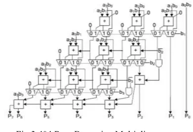
A low-power row-bypassing multiplier is also proposed to reduce the power consumption and use of more clock cycles. The operation of the low-power row-bypassing multiplier is similar to that of the low-power column bypassing multiplier, but the selector of the multiplexers and the tri-state gates use the multiplication. The design of 4*4 row bypassing multiplier is shown in Fig.3. The basic concept is to execute a shorter path using a shorter cycle and longer path using two cycles. Since most paths execute in a cycle period that is much smaller than the critical path delay, the variable latency design has smaller average latency. Each input is connected to full adder through a tri-state gate. When the inputs are 1111 * 1001, the two inputs in the first and second rows are 0 for full adders. Because is 0, the multiplexers in the first row select aib0 as the sum bit and select 0 as the carry bit. The inputs are bypassed to full adders in the second rows, and the tri-state gates turn off the input paths to the full adders.
Fig.3 4*4 Row Bypassing Multiplier
(D) Variable Latency Design
The variable-latency design was proposed to reduce the timing waste occurring in traditional circuits that use the critical path cycle as an execution cycle period cycles as shown in Fig.4. The basic concept is to execute a shorter path using a shorter cycle and longer path using two cycles. Since most paths execute in a cycle period that is much smaller than the critical path delay, the variable-latency design has smaller average latency. Fig.4 is an 8-bit variable-latency ripple carry adder (RCA). A8–A1, B8–B1 is 8-bit inputs, and S8–S1 are the outputs.
Supposing the delay for each full adder is one, and the maximum delay for the adder is 8.Through simulation, it can be determined that the possibility of the carry propagation delay being longer than 5 is low. Hence, the cycle period is set to 5, and hold logic is added to notify the system whether the adder can complete the operation within a cycle period.
Fig.4: 8-bit RCA with a hold logic circuit.
IV EXISTING METHOD
Fig.5 Multiplier design with Adaptive hold logic
multiplication to predict whether the operation requires one cycle or two cycles to complete.
V PROPOSED RELIABLE MULTIPLIER
(A) Proposed model
The multiplier architecture, which includes two m-bit inputs (m is a positive number), one 2m-m-bit output, one column- or row-bypassing multiplier, 2m 1-bit Razor flip-flops and an AHL circuit as shown in Fig.6. The column- and row-bypassing multipliers can be examined by the number of zeros in either the multiplicand or multiplication to predict whether the operation requires one cycle or two cycles to complete. When input patterns are random, the number of zeros and ones in the multiplication and multiplicand follows a normal distribution. Therefore using the number of zeros or ones as the judging criteria results in similar outcomes. Hence, the two multipliers can be implemented using similar architecture, and the difference between the two bypassing multipliers lies in the input signals of the AHL. According to the bypassing selection in the column or row bypassing multiplier, the input signal of the AHL in the architecture with the column-bypassing multiplier is the multiplicand, whereas that of the row-bypassing multiplier is the multiplication.
Fig.6 Multiplier design with Adaptive hold logic
Fig.7 Razor Flip Flop
(B) Razor Flip Flop
Razor flip-flops can be used to detect whether timing violations occur before the next input pattern arrives as shown in Fig.7. A 1-bit Razor flip-flop contains a main flip-flop, shadow latch, XOR gate, and multiplexer. The main flip-flop catches the execution result for the combination circuit using a normal clock signal, and the shadow latch catches the execution result using a delayed clock signal, which is slower than the normal clock signal. If the latched bit of the shadow latch is different from that of the main flip-flop, this means the path delay of the current operation exceeds the cycle period, and the main flip-flop catches an incorrect result. If errors occur, the Razor flip-flop will set the error signal to 1 to notify the system to re execute the operation and notify the AHL circuit that an error has occurred.
(C) Adaptive Hold Logic
The AHL circuit is the key component in variable-latency multiplier. Fig.8 shows the details of the AHL circuit. The AHL circuit contains an aging indicator, two judging blocks, one multiplexer, and one D flip-flop. The aging indicator indicates whether the circuit has suffered significant performance degradation due to the aging effect. When input patterns arrive, the column- or row-bypassing multiplier, and the AHL circuit execute simultaneously.
According to the number of zeros in the multiplicand (multiplication), the AHL circuit decides if the input patterns require one or two cycles. If the input pattern requires two cycles to complete, the AHL will output 0 to disable the clock signal of the flip-flops. Otherwise, the AHL will output 1 for normal operations. When the column- or row-bypassing multiplier finishes the operation, the result will be passed to the Razor flip-flops.
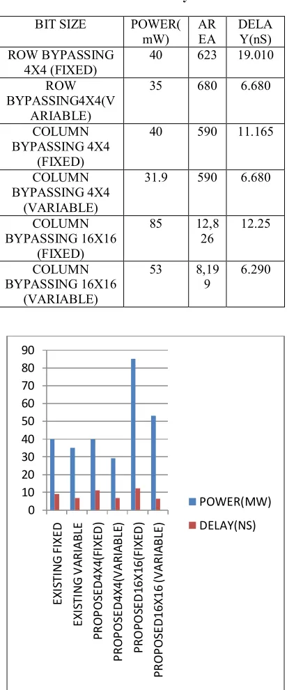
In the below Table.1 the fixed latency and variable latency are compared for power and delay. In the fixed latency the more number of clock cycles are required and due to which the area, power and delay are increased. By using proposed adaptive hold logic i.e., in the variable latency the less number of clock cycles are used and due to which the error is reduced so that the area, power and delay are reduced in variable latency.
Table.1 Comparison Result of Fixed and Variable Latency
BIT SIZE POWER(
mW) AR EA DELA Y(nS) ROW BYPASSING 4X4 (FIXED)
40 623 19.010
ROW BYPASSING4X4(V
ARIABLE)
35 680 6.680
COLUMN BYPASSING 4X4
(FIXED)
40 590 11.165
COLUMN BYPASSING 4X4
(VARIABLE)
31.9 590 6.680
COLUMN BYPASSING 16X16
(FIXED)
85 12,8 26
12.25
COLUMN BYPASSING 16X16
(VARIABLE)
53 8,19 9
6.290
Figure 9 Performance analyses of the Multipliers.
VI SIMULATION RESULT
The simulation result of fixed and variable latency for row and column bypassing is shown.
Fig10: row multiplier 4x4 Result
Fig11: column multiplier 4x4 Result
VII CONCLUSION
This paper proposed a reliable variable-latency multiplier design with the AHL. In the fixed latency the clock cycles is fixed and due to this the timing violations occur. To overcome this problem variable latency is used to reduce the delay. The experimental results show that our proposed variable latency design has reduced delay for 8×8 and 16×16 for column-bypassing multipliers and row bypassing multipliers of 4X4 when compared to fixed latency. The delay of 16*16 fixed column bypassing is 11.165(ns) are reduced to 6.80(ns) in variable latency. The delays of 4X4 fixed row bypassing are 19.010(ns) are reduced to 6.80(ns) in variable latency. The power of 16*16 for column bypassing fixed latency is reduced by using variable latency design and same for row bypassing fixed latency is reduced by using variable latency design. As error occurred due to timing violations is reduced by reliable multiplier using adaptive hold logic.
REFERENCES
[1] Y. Cao. (2013). Predictive Technology Model (PTM) and NBTI Model [Online]. Availablehttp://www.eas.asu.edu/ptm [2] S. Zafar, A. Kumar, E. Gusev, and E. Cartier, “Threshold voltage instabilities in high-k gate dielectric stacks IEEE tran DeviceMater Rel., vol. 5, no. 1, pp. 45–64, Mar. 2005. [3] K. Du, P. Varman, and K. Mohanram, “High performance reliable variable latency carry select addition,” in Proc. 2012, pp. 1257–1262.
[4] J.sudha rani and R.N.S.Kalpana , “ Design of Low Power Column bypass Multiplier using FPGA” International Journal Of Computational Engineering Research (ijceronline.com) Vol. 3 Issue. 2
[5] Sharvari San and Tantarpale, “Low-Cost Low-PowerImproved Bypassing-Based Multiplier” IJCSCE Special issue on “Recent Advances in Engineering & Technology” NCRAET- 2013
Gaminidi Monika 14ND1D5703
M.Tech Student Scholar Fathr name:Nageswararao
Department of Electronics & Communication Engineering,
St.Mary’s Women’s Engineering College, Budampadu, Guntur district, A.P, India.
+91 8121426426
K.Sreenivasa Rao, Asst.professor,
Department of Electronics & Communication Engineering,
St.Mary’s Women’s Engineering College, Budampadu, Guntur district, A.P, India.