Design and Analysis of Band-Reject 3-D
Frequency Selective Surface with Multiple
Transmission Zeros and Pseudo-Elliptic
Response
Vishumendra Thakur
1, Bimal Raj Dutta
2, Binod Kumar Kanaujia
3PG Student [Microwave], Dept. of ECE, Shri Ram Murti Smarak College of Engineering & Technology, Bareilly, (U.P) India1
Head of Department, Dept. of ECE, Shri Ram Murti Smarak College of Engineering & Technology, Bareilly, (U.P) India2
Head of Department, Dept. of ECE, Ambedkar Institute of Advanced Communication Technologies & Research, Delhi, India3
ABSTRACT: The designed three-dimensional Frequency Selective Surface (FSS) with multiple transmission zeros and pseudo-elliptic response is constructed from two-dimensional periodic array of shielded microstrip lines. Unlike the traditional two dimensional FSS, the designed three dimensional FSS exhibits pseudo-elliptic band-reject (6GHz - 14GHz) response. As the plane wave of linear polarization incidents perpendicularly to the shielded microstrip line with perfect electric conductor (PEC) and perfect magnetic conductor (PMC) boundary walls, two quasi-TEM modes are obtained namely air and substrate mode. The designed 3D FSS is a combination of two or more resonators from which the in phase combination of the modes gives transmission poles and out of phase combination of the modes gives transmission zeros respectively. This 3D FSS is designed and simulated using Ansys HFSS software. The obtained verified result shows that the 3D FSS exhibits improved performance over 2D FSS, for many practical applications such as antenna sub-reflector, radomes and spatial filters.
KEYWORDS: Frequency Selective Surface (FSS), microstrip line, resonators, multiple transmission zeros, pseudo-elliptic response, perfect electric conductor (PEC), perfect magnetic conductor (PMC).
I. INTRODUCTION
A new concept of 3-D Frequency Selective Structure (FSS) has been a recent topic of research where multiple transmission poles/zeros can be produced with multimode resonators. On this concept number of 3-D FSSs based on a 2-D periodic array of shielded microstrip line resonators was proposed. One such design from which our work in this paper is related is a 2-D periodic array of shielded microstrip line having shorting via (connecting microstrip to the ground) [5] which gives a band-reject 3-D FSS structure.
Fig. 1. Multiple resonators and cross-coupling between source and load to obtain transmission poles/zeros at finite frequencies
With a new concept of 3D frequency selective surface multiple transmission poles/zeros will be produced through multimode resonators. A case of band-reject pseudo-elliptic filtering response with dual-band rejection and broadband rejection has been thoroughly studied for planar microstrip filters. By introducing transmission zeros at desired finite frequencies wide band rejection will be realized. This 3D FSS consists of a 2D periodic array of shielded microstrip lines placed vertically supporting the quasi-TEM modes namely the air and substrate mode. These modes are generated when a linearly polarized plane wave is incidented perpendicularly to the microstrip at the air-to-microstrip line discontinuity.
Fig. 2. 3D FSS with single air mode resonator and two substrate mode resonators
In this paper two 3D FSS designs have been presented with the first design of dual-band band-reject characteristics having a shielded microstrip lines with PEC and PMC boundary wall along with a single shorting via that constitutes of total three resonators (one air mode resonator and two substrate mode resonators) as shown in Fig. 2. The second design is of broad-band band-reject characteristics which are geometrically modified from the first design with the inclusion of three more shorting via those results in the increase of the band-reject frequency. This increase is due to the addition of more number of shorting via at the center of the microstrip.
II. PRINCIPLE OF OPERATION
We can represent a 3D FSS by an equivalent model as shown in Fig. 3. For simplification we consider a model of four resonators 𝑅1, 𝑅2, 𝑅3 and 𝑅4 that are linking input and output port, whereas resonators 𝑅𝑎 and 𝑅𝑏 are linked only to
Fig. 3. Equivalent model of a 3D FSS having multiple resonators
Each resonator represents a propagating mode that provides either a transmission zero or transmission pole at their respective resonant frequencies. Resonator 𝑅𝑎, 𝑅𝑏, 𝑅𝑐 and 𝑅𝑑 provide additional transmission zeros at the desired
frequencies thus increasing the bandwidth of a band-stop FSS or improving the selectivity of a band-pass FSS. Thus 3D FSS provides flexibility in producing desired number of transmission zeros/poles at finite frequencies by controlling the number of resonators and their resonances, therefore 3D FSS have quasi-elliptic filtering response [4].
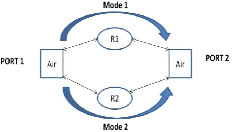
2D FSS are the special case of this equivalent model of 3D FSS consisting of only one resonator or mode that provides a single transmission zero/pole which leads to poor filtering performance. Principle of operation of these 3D FSS needs to be reviewed to understand how the resonators are formed. When a plane wave having an electric field (TE polarization) oriented perpendicular to the shielded microstrip incidents at the air-to-microstrip line discontinuity, two propagating modes [6] are created namely air and substrate modes that link input and output ports. At low frequencies the incident signals travel through the air path from one port to other providing low-pass response, but as the frequency of operation increases the same signal travels through two paths (air and substrate). The substrate mode resonator will always resonate first than the air mode resonator since the guided wavelength (𝜆𝑔) of the substrate mode is less than the
air mode (𝜆0). In such propagating modes of air and substrate there are two possibilities: (a) the first being the
generation of transmission poles which is produced whenever the electrical length of any resonator becomes equal to 𝜋, (b) the second being the generation of transmission zeros which is produced whenever the phase difference between signals in the air and substrate path is 1800.
Fig. 4. Equivalent model of a 3D FSS having two resonators/modes
There are two modes present in the equivalent model as shown in Fig. 4. Here the two transmission poles are obtained due to the two resonators ( 𝑅1, 𝑅2), which are resonating at their resonant frequencies. Also one transmission zero is
obtained at a frequency where the two modes are 1800 out of phase.
III. FIRST DESIGN (BAND-REJECT FSS)
A. Structure Description
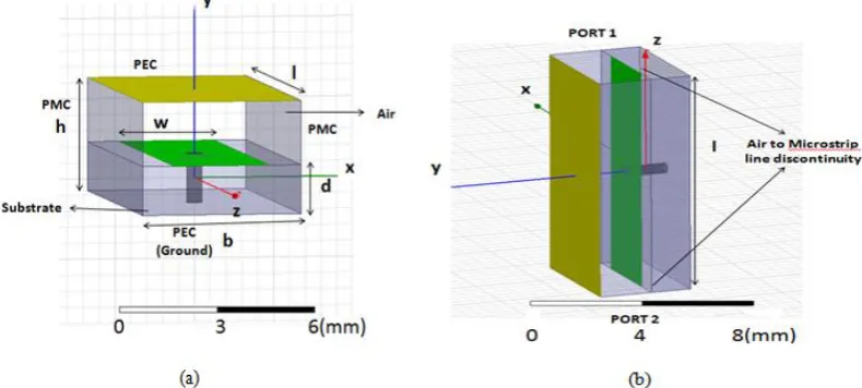
Fig. 5. Three-dimensional view of the bandstop FSS (a) side view (b) top view
The array shown in Fig 5(a) is a combination of 4x4 unit cells. Each unit cell as shown below in Fig 6(a) has the height in y direction h = 3.524mm, which is a combination of air and substrate region. The height of the substrate in y direction is d = 1.524mm. The length of the unit cell/microstrip line in z direction is l = 10.5mm. The width of the unit cell/substrate in x direction is b = 5mm. The substrate material incorporated in the design is Rogers RO3003 having dielectric constant of value 3.
Fig. 6. Three-dimensional view of a unit cell of (a) top view (b) side view
As shown in the Fig. 6(a) the width of the microstrip line in x direction is w = 3mm. The design also includes a shorting via of diameter D = 0.5mm that connects ground to the center of microstrip line. The unit cell reappears after a period of “b” in x direction and “h” in y direction. It is having a PEC boundary in x-z plane and PMC boundary y-z plane. The plane wave with TE polarization travelling in z direction will be incident at port 1 (air to microstrip line discontinuity) as shown in Fig 6(b).
B. Equivalent Circuit Model Analysis
Fig. 7. Block diagram showing the transfer matrix of the first sub network (air path)
The A, B, C, D parameters of the transfer matrix are used to realize the impedance parameters of the impedance matrix 𝑍 . Thereby with the aid of impedance parameters, the scattering parameters of the 𝑆 matrix are realized [5, 2]. The A, B, C, D parameters of the transfer matrix of the Fig. 7 sub network depend on the equivalent lumped Capacitor (𝐶𝑎), transmission line parameter i.e. characteristic impedance of the air path ( 𝑍𝑎) and the electrical length of
the air path (𝛩𝑎). The capacitor 𝐶𝑎 is used to represent the discontinuity between the air region of the unit cell and the
air region outside the unit cell.
Fig. 8. Block diagram showing the transfer matrix of the second sub network (substrate path)
The block diagram of the substrate path sub network as per Fig. 8, represents the transfer matrix of each section, an overall transfer matrix of the substrate path network is resulted due to cascading of the each block. The A, B, C, D parameters of the transfer matrix of the substrate path sub network shown in Fig. 8, depend on the following (a) two equivalent lumped elements i.e. Capacitor (𝐶𝑠) and Inductor 𝐿𝑠 (b) transmission line parameter i.e. characteristic
impedance of the substrate path ( 𝑍𝑠) (c) the electrical length of the substrate path (𝛩𝑠).
The capacitor 𝐶𝑠 is used to represent the discontinuity between the substrate region of the unit cell and the air region
outside the unit cell. The inductor ( 𝐿𝑠) represents the shorting via that connects ground to the microstrip.
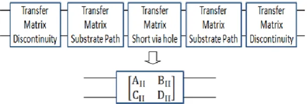
Fig. 9. Block diagram showing the cascaded combination of the transfer matrix of the two sub network (air and substrate path)
The equivalent transfer matrix of the two sub network is cascaded as shown above in Fig. 9, to realize the impedance parameters of the equivalent circuit model [5] which are as follows
𝑍11 = 𝑍22= 𝐴𝐼
𝐶𝐼+ 𝐴𝐼𝐼
𝐶𝐼𝐼 (1a)
𝑍12 = 𝑍21= 1 𝐶𝐼+
1
𝐶𝐼𝐼 (1b)
𝐶𝑎 ≈ 𝑤 𝑏
ℎ
𝜔 ℎ −𝑑 𝑍0𝑡𝑎𝑛 ∆𝛩 (3a)
𝐶𝑠 ≈ 𝜀𝑟 𝑤 𝑏
ℎ
𝜔𝑑 𝑍0𝑡𝑎𝑛 ∆𝛩 (3b)
𝐿𝑠= 𝜇0
2𝜋 𝑑 𝑙𝑛2
𝑑+ 𝐷2 2+𝑑2
𝐷 + 1.5
𝐷 2−
𝐷 2
2
+ 𝑑2 (3c)
Here 𝑍0 is the characteristic impedance of the parallel plate waveguide that represents the free space region outside the
unit cell carrying the TE polarized plane wave. The 𝑡𝑎𝑛 ∆𝛩 is evaluated from [5] as follows
𝑡𝑎𝑛 ∆𝛩 = 2ℎ
𝜆 ℎ−𝑑 ℎ 𝑙𝑛 ℎ ℎ−𝑑+ 𝑑 ℎ 𝑙𝑛 ℎ 𝑑 + 𝑆1
2ℎ
𝜆 ; 0,0 − 𝑆1 2 ℎ −𝑑
𝜆 ; 0,0 − 𝑆1 2𝑑
𝜆 ; 0,0 (3d)
Where
𝑆1 𝑥; 0,0 = 𝑠𝑖𝑛−1 𝑥 𝑛 −
𝑥 𝑛 ∞
𝑛=1 (3e)
The propagation constant of the air mode 𝛽𝑎 and the substrate mode 𝛽𝑠 are evaluated from [12], thereby the electrical
length of these two modes are realized as follows
Air mode 𝛩𝑎 = 𝛽𝑎𝑙 (4a)
Substrate mode 𝛩𝑠= 𝛽𝑠𝑙 (4b)
C. Design Methodology
The basic design guidelines for the efficient designed 3D FSS are as follows:
The width b and the height h of the unit cell should be much smaller than the operating wavelength (32.6mm). This results in stable frequency response under variation of the angle of incidence (00-600).
The value of 𝜀𝑟 plays a vital role in deciding whether the designed 3D FSS is narrowband or wideband FSS. A
low value of 𝜀𝑟 results in single transmission zero (narrowband FSS), while large value of 𝜀𝑟 results in two or more
transmission zeros (wideband FSS).
The length of the microstrip is calculated as
𝐿 =𝜆𝑔
2 = 𝜆0
2 𝜀𝑟𝑒 (5a)
Where 𝜆𝑔 is the guided wavelength at the required center frequency of the FSS and 𝜀𝑟𝑒 is the effective dielectric
constant.
For the microstrip of thickness t→0 and w/d ≥ 1 ,the value of 𝜀𝑟𝑒 is evaluated [2] as follows
𝜀𝑟𝑒 = 𝜀𝑟+1
2 +
𝜀𝑟−1
2 1 + 12 𝑑 𝑤
−0.5
(5b) the value of 𝜀𝑟𝑒 is a function of frequency and its value lies between
1 < 𝜀𝑟𝑒 < 𝜀𝑟 (5c)
as the frequency of operation increases 𝜀𝑟𝑒 approaches 𝜀𝑟.
IV. SECOND DESIGN (IMPROVED BAND-REJECT FSS)
A. Structure Description
Previously designed 3D band-reject FSS had a dual band band-reject frequency which could not effectively reject the entire required band of frequencies. Also the frequency response achieved was not close to the quasi-elliptic response behaviour.
(a) (b)
Fig. 10. Three-dimensional view of the improved band-reject FSS (a) side view (b) top view
A new 3D FSS has been designed as shown above in Fig 10 (a,b) that overcomes the shortcoming of the previous design. The physical dimensions of this design are similar to the previous designs. Here the array is also a combination of 4x4 unit cells consisting of a shielded microstrip. The difference is seen in the construction of the unit cell which has four shorting via connecting ground to the microstrip instead of having a single shorting via.
(a) (b)
Fig.11. Three-dimensional view of the unit cell of the improved band-reject FSS (a) top view (b) side view
All four of these shorting via are placed at an equal distance from each other along the x axis under the center of the microstrip as shown in Fig. 11 (a,b). The top and side view of this design are shown in Fig. 11
V. RESULTS AND DISCUSSION
A. Analysis of Simulated Result for the First Design 3D band-reject FSS
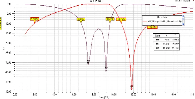
Fig. 12.Simulated S parameter results from HFSS for the bandstop FSS
The graph shown in Fig. 12 is a combination of S11 (Reflection Coefficient) and S21 (Transmission Coefficient)
parameters, which are the simulated results of the equivalent two port device of a unit cell. Here Floquet port excitation has been provided in z direction on port 1 and port 2. It results in three resonance frequencies. The two of them are the transmission zero at frequencies 5.4GHz and 9.6GHz due to substrate mode resonators. The third one is transmission pole at frequency 13GHz due to air mode resonator. It is observed that the band-reject frequency of this 3D FSS has been increased by the addition of an extra transmission zero which is obtained by the inclusion of shorting via. This short via introduces an extra short-circuit resonator in addition to existing open-circuit microstrip line resonator [5].
B. Analysis of Simulated Result for the second design 3D band-reject FSS
The simulated S parameter results as shown in Fig. 13, is used to analyse the improved band-reject characteristics of this 3D FSS..
Fig.13. Simulated S parameter results from HFSS for the improved band-reject 3D FSS
The graph shown above is a combination of reflection and transmission coefficient (𝑆11, 𝑆21). In this graph also we get
PARAMETERS FIRST DESIGN SECOND DESIGN
Bandwidth of the band-reject FSS Dual-band band-reject obtained of (1.) 0.8GHz (2.) 0.7GHz
Single broad-band band-reject obtained of 3GHz
Transmission pole frequency 13GHz 11.8GHz Elliptical Response Less elliptical More elliptical
Table 1 Comparison between the first and second design
Table 1. shown above is a comparison between the first and second design. The bandwidth of the band-reject FSS for the first design is much narrower than the second design having dual band of bandwidth 0.8GHz and 0.7GHz whereas for the second design the bandwidth obtained is broad (3GHz). Also the frequency response of the second design is more elliptical with a transmission pole frequency occurring at 11.8GHz as compared to the transmission pole frequency (13GHz) of the first design.
VI. CONCLUSION
Two 3D band-reject FSS have been presented that are 2D periodic array arrangement of shielded microstrip line. The first design with only single short via shows dual narrowband band-reject 3D FSS with quasi elliptic response. The second design with four short via shows a broadband band-reject 3D FSS with more elliptic response than the former design. Thus 3D FSS allows greater operating bandwidth than 2D FSS with inclusion of more transmission zeros and also improves the selectivity of the operating bandwidth.
REFERENCES
[1] B.A.Munk, Frequency Selective Surfaces: Theory and Design. New York, NY, USA: Wiley, 2000. [2] David M. Pozar, “Microwave Engineering”, John Wiley & Sons,Inc.
[3] J.S. Hong and M. J. Lancaster, “Microstrip Filter for RF/Microwave Applications”. New York, NY, USA: Wiley, 2001.
[4] A. K. Rashid, Z. Shen, and B. Li, “An elliptical bandpass frequency selective structure based on microstrip lines,” IEEE Transactions on Antennas and Propagation, Vol. 60, Issue no. 10, pp. 4661–4669, Oct. 2012.
[5] Bo Li and Z. Shen, “Three-dimensional bandpass frequency-selective structures with multiple transmission zeros,” IEEE Transactions on Microwave Theory and Techniques,Vol. 61, Issue no. 10, Oct. 2013.
[6] A. K. Rashid and Z. Shen, “A novel band-reject frequency selective surface with pseudo-elliptic response,” IEEE Transactions on Antennas and Propagation, Vol.58, Issue no. 4, pp. 1220–1226, Apr. 2010.
[7] A. K. Rashid, Z. Shen, and S. Aditya, “ Wideband microwave absorber based on a two dimensional period array of microstrip lines,” IEEE Transactions on Antennas and Propagation, Vol. 58, Issue no. 12, pp. 3913–3922, Dec. 2010.
[8] S. Amari, U. Rosenberg, and J. Bornemann, “Adaptive synthesis and design of resonator filters with source / load-multiresonator coupling,” IEEE Transactions on Microwave Theory and Techniques, Vol. 50, Issue no. 8, pp. 1969–1678, Aug.2002.