4th of July, 2014
MASTER THESIS
A
PLUG
BASED
MICRO SOLID PHASE
EXTRACTION
(
µ
SPE)
MICROFLUIDIC
CHIP
FOR THE ISOLATION
AND PURIFICATION OF
DNA
ing. H.W. (Henk-Willem) Veltkamp
Faculty of Science and Technology (TNW, Technische Natuurwetenschappen) Mesoscale Chemical Systems (MCS)
Exam committee:
“DNATECHNOLOGY COULD BE THE GREATEST SINGLE ADVANCE IN THE SEARCH FOR TRUTH,
CONVICTION OF THE GUILTY,
AND AQUITTAL OF THE INNOCENT SINCE THE ADVENT OF CROSS-EXAMINATION.”
Preface
Last academic year was the climax of my Master’s degree, namely the Master’s thesis. About 15 months ago I started looking for a research group where I wanted to do my thesis research. That group was found quite quickly. Already two years back I sort of decided that I wanted to do my Master’s thesis re-search in the Mesoscale Chemical Systems rere-search group of the MESA+Institute for Nanotechnology, after doing my University of Applied Sciences internship there. After discussing some possible topics I have chosen for the forensic/DNA related topic.
During my Master’s thesis, I learned a lot. The field of forensics and DNA related analysis was new for me, so it was a real challenge to learn the basics of it in the shortest period of time possible. But once this was done, I had a good basis to work with. The literature study learned me a lot about the different on-chip extraction methods used for DNA extraction. During the design part of this thesis research, I learned to work with both COMSOL MultiPhysics and CleWin 5 mask designing software. The practical work can be divided into two parts, the clean room work and the work that is done in the chemical lab of the Mesoscale Chemical Systems research group. During the clean room work, I followed as much clean room courses as possible. This resulted in a skill set with almost every important step inside the MESA+ clean room. This skill set is very valuable in my future career. A complete overview of all the followed courses can be found in appendix L. During the practical work in the chemical lab, I also helped to move our chemical lab from the Meander building to the Carr ´e building. This change of labs was necessary because of the shortage of space due to new group members. This learned me a lot about safety in the lab and chemical waste disposal.
Now, I have almost finished my Master completely and I am looking back on a wonderful time. This wonderful time resulted in the now following thesis and I hope that you will have as much fun as I had writing it.
J.1 DataPhysics OCA 15plus contact angle system . . . 117
K.1 Extraction test with chitosan coating and TRIS pH 9.2 . . . 121
K.2 Extraction test with APTES coating and TRIS pH 9.2 . . . 121
List of Tables
2.1 Channel (ch) and pillar (p) areas (A) and volumes (V). . . 19
4.1 XPS results chitosan functionalization . . . 45
4.2 XPS results APTES functionalization . . . 46
4.3 Results of contact angle measurements . . . 47
4.4 Summarized results of the extraction tests . . . 51
4.5 Validation of the Qubit dsDNA HS assay kit . . . 52
D.1 Results of pH measurements . . . 96
Abbreviation Description
O/W oil in water
PANAM poly-amidoamine
PC polycarbonate
PCI phenol/chloroform/isoamyl alcohol PDMS polydimethylsiloxane
PEEK polyether ether ketone PETG polyethylene terephthalate PMMA poly(methylmethacrylate)
PS polystyrene
PTFE polytetrafluoroethylene RNA ribonucleic acid
Si silicon
TEOS tetraethyl orthosilicate TMOS tetramethyl orthosilicate
TRIS tris(hydroxymethyl)methylamine hydrochloride
W/O water in oil
Chapter 1
Introduction
This chapter gives first general background information about microfluidics and the lab-on-a-chip con-cept, followed by the Master’s thesis problem description, the approach used to solve this problem and a literature survey of the state-of-the-art.
1.1
Microfluidics and the lab-on-a-chip concept
The start of microfluidics, i.e. the handling and studying of fluids in the nanolitre to attolitre (10-9 to 10-18L) range (length scales less than a millimetre, hence the name microfluidics), was in the early 1950’s when the basics were established for the modern ink-jet technology. The real revolution came when the first miniaturized gas chromatograph was realized by Terry et al.[1], which is shown in
fig-ure 1.1. A little bit more than a decade later, in 1990 to be precise, Manz et al. introduced for the first time the term micro total analysis system (µTAS)[2], together with a microfluidic liquid
chromatog-raphy device, fabricated using Si-Pyrex technology[3]. A photograph of this device is also shown in
figure 1.1. The term which is nowadays more common is lab-on-a-chip (LoC). The use of this word started in 1995 when Moser et al. published an article about glutamate and glutamine biosensors[4].
This broad term covers a range of special classes of miniaturized devices: lab-on-a-chip, biochips, bio-micro-electro-mechanical systems (bioMEMS), microreactors, and point-of-care devices, just to name a few. They all have the same aim, namely to control concentrations of molecules in time and space. All these different classes are the result of a highly interdisciplinary field of research. This multidisci-plinary character is visible in the broad range of scientific journals publishing about microfluidics,µTAS, and LoC (e.g.Lab-on-a-Chip, Sensors and Actuators, Analytical Chemistry, Journal of Micromechanics and Microengineering, and Applied Physics Letters). The development of number of publications per year on the topics of microfluidics, micro total analysis system, and lab-on-a-chip is shown in figure 1.2. These graphs clearly indicate that it is a development of the last 15 years. The start of this development can be coupled to the Defence Advanced Research Projects Agency (DARPA) of the US Department of Defence. This agency supported in the 1990’s the development of field-deployable microfluidic systems that can be used for the detection of chemical and biological threats[5].
Master’s thesis
Figure 1.2: The amount of publications per year on A) microfluidics, B) micro total analysis system, and C) lab on a chip, lab-on-a-chip, lab on chip, lab-on-chip found in the renowned databases of Elsevier’s Scopus[6]and Thomson Reuters’ Web of Science[7].
A variety of other microfluidic devices and structures, such as microvalves[8] and micropumps[9],
Master’s thesis early adulthood:
”HOWEVER,ITS IMPACT ON SCIENCE HAS NOT YET BEEN REVOLUTIONARY. REVOLUTIONS IN
TECHNOLOGY REQUIRE BOTH A BROAD RANGE OF DIFFERENT TYPES OF COMPONENT AND
SUBSYSTEM,AND THEIR INTEGRATION INTO COMPLETE,FUNCTIONAL SYSTEMS.THE FIELD OF
MICROFLUIDICS IS IN EARLY ADOLESCENCE,AND STILL LACKS BOTH THESE ESSENTIAL
REQUIREMENTS,IN ADDITION TO THE INTEGRATION OF COMPONENTS INTO SYSTEMS THAT CAN BE
USED BY NON-EXPERTS. AS A FIELD,IT IS A COMBINATION OF UNLIMITED PROMISE, PIMPLES AND INCOMPLETE COMMITMENT. THIS IS A VERY EXCITING TIME FOR THE FIELD,BUT WE STILL DO NOT
KNOW EXACTLY WHAT IT WILL BE WHEN IT GROWS UP.”
1.2
Assignment description
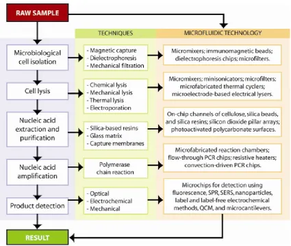
The problem investigated in this master thesis is the problem of analysing forensic samples found on the crime scene. The current method is that a crime scene investigator collects every potential interest-ing sample and sends this to the Dutch Forensic Institute (Nederlands Forensisch Instituut, NFI) in The Hague (NL). Once the samples are there, they start to work up the samples,i.e. purifying the sample, performing cell lysis, collection of DNA, performing a multiplication reaction on the DNA, and finally making a short tandem repeat (STR) profile of the DNA. A general DNA analysis scheme is shown in figure 1.4.
Figure 1.4: Flow-chart of chip-based DNA isolation, extraction, amplification, and detection. The name of the step is on the left, the traditional method steps are in the middle, and the translation to microfluidic technology is in the right column. Picture taken from reference 49.
Master’s thesis
Figure 1.7: Schematic representation of a capillary-basedµSPE device. Picture taken from reference 48.
1.3.2
Monolithic columns
The porous polymer approach uses capillaries or columns that have been filled with a porous polymer structure. Such chromatographic supports are called monoliths[101]. These type of supports were
intro-duced in the late 1980’s and early 1990’s[102,103]. The use of a monolith in aµSPE device is proposed
by Yu et al.[93] and is based on the work of Svecet al.[104–106]. In order to fill the capillary or column
with the porous polymer, a solution of monomers and initiator in a porogenic solvent is injected into the capillary and these monomers are polymerised by photo-initiation by UV exposure[93,100]or thermal
ini-tiation[100]. The monomer choice determines the final properties of the porous structures. Examples of
these properties are the hydrophobicity, surface charge, and functionalization possibilities[107,108]. Two
of the largest advantages of such a monolithic porous structure is the high surface-area-to-volume ratio and the accurate placement of the monolith matrices within the microfluidic device due to local poly-merization by UV or heat[93,100,109]. A scanning electron microscope (SEM) image of such a porous
polymer-filled column is shown in figure 1.8. However, the extraction efficiencies of DNA purification and separation performed in such systems is low and it requires high salt and pH buffer for the DNA re-lease[101]. These low extraction efficiencies can most probably be addressed to the low reproducibility of the polymerization reaction, the same problem as with the sol-gel reaction described before. Moreover, the required buffers are not suitable for PCR amplification because of their high salt concentration[100].
Figure 1.8: A porous polymer-filledµSPE column, with a) microfluidic chip layout, and b) SEM image of a monolithic ion-exchange concentrator (µSPE column). Picture taken from reference 93.
This method is not only limited to silicon or glass capillaries. Stachowiaket al.fabricated such mono-lithic porous structures inside a plastic microfluidic device[94]. The main disadvantage of this method is the device-to-device reproducibility of the monolith.
Wen et al. designed aµSPE chip with two regions, a protein binding C18 reversed phase column and a monolith made out of the monomer 3-(trimethoxysilyl)propyl methacrylate, which was functional-ized with TMOS[79]. The C18 reversed phase column captures most of the, mostly hydrophobic, proteins
from whole blood samples, such as haemoglobin, while having a minimal binding with DNA. This en-sures a more effective extraction of DNA in theµSPE column. They achieved an extraction efficiency of 69±1% for their combined system. However, the TMOS functionalization requires chaotropic con-ditions in order to perform its function, making it not suitable for PCR on chip[10,76,79,84,85]. This is a
Master’s thesis
Figure 1.9: The integrated protein capturing C18 reversed phase column and the DNAµSPE column. The arrows show the flow direction for the different steps in the process and the percentages show the mass balance through the system. Picture taken from reference 79.
problem Wenet al. encountered during their research. The chip designed by Wen et al. is shown in figure 1.9.
1.3.3
One-piece columns
This method has the most simple production process of the three different methods. Here, the solid phase is shaped directly into the substrate material by etching. A surface functionalization can be done afterwards, but is not always necessary, for example in the case with DNA extraction with silica surfaces and chaotropic salts[83]. The two most typical structures for this kind of extraction are an array
of micropillars, which can be present in all kinds of shapes (see figure 1.11 and 1.12[95,98]and one[110]
or multiple parallel channels[111](see figure 1.10). Pillars are in this case used to increase the
surface-area-to-volume (SA-V) ratio of the column. The concept of using pillars for DNA extraction was firstly demonstrated by Christelet al. in 1999[112]. The direct etching of the solid phase into the substrate
circumvents the problems that are associated with the filling of the channels with binding matrices, which needs to be done after the fabrication of the device[49].
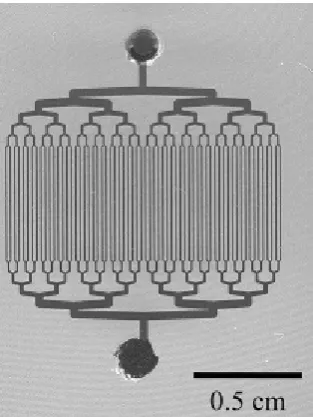
Figure 1.10: Picture of a SPE device based on parallel channels. Picture taken from reference 111.
The method demonstrated by Cady et al.[83] is based on the increase in surface area by adding pillars in the microfluidic channel. With these pillars, they increased the surface area within the channel with 300-600%. The silica surface of the pillars and channels allowed DNA extraction with the use of a chaotropic salt. A binding capacity of approximately 82 ng cm-2has been reported, but only 10% of the
Master’s thesis
Figure 1.11: An polymer-based extraction chip, with a) photograph of the complete chip, with PDMS covering and tubing, and b) SEM image of the epoxy-based pillars in the DNA purification region. Picture taken from reference 98.
Figure 1.12: SEM image of an array of micropillars etched in silicon. Picture taken from reference 95.
Master’s thesis
1.4
Approach in this thesis research
The approach chosen in this research is based on pH-induced extraction via an ion exchange func-tionalization inside an etched column. This approach is chosen primarily because of the fact that a complete aqueous based method can be established, removing the use of chaotropic salts and other exogenous PCR inhibitors. Also, this approach has a better fabrication reproducibility when compared to beads-filled columns and monolithic columns. The idea is to design aµSPE column that can extract DNA and subsequently elute it in a plug of aqueous buffer. This buffer plug is the smallest amount of buffer needed to extract the DNA from the column. For this it is necessary to have a straight plug profile inside the column, such that the DNA gets eluted over the whole width of the column, more or less at the same time. This plug profile can be established with the use of a flow distributor before the column. The substrate of choice is a hybrid substrate with a silicon and a silica layer. These substrate are chosen because of their robustness, reproducibility, and available equipment in the MESA+clean room. A more
Chapter 2
Theoretical aspects
The second chapter of this thesis introduces the reader into all design aspects for theµSPE chip de-veloped in this project. This chapter starts with the theoretical design of the chip. This paragraph is followed by a paragraph about the mathematical aspects of microfluidics and finite element methods-based computational fluid dynamics. Then, a short paragraph about surfactants and their role in water-in-oil emulsions. This theory is related to the buffer plug formation in the oil stream. The chapter closes with a paragraph is dedicated to the used DNA detection method. Measuring low concentrations of DNA is often quite troublesome[174], so it is good to spend a small paragraph on this matter. The choice is
made to not discuss the theoretical aspects of the different fabrication steps here, since it is considered basic knowledge. The interested reader who wants more information on this subject can read appendix A.
2.1
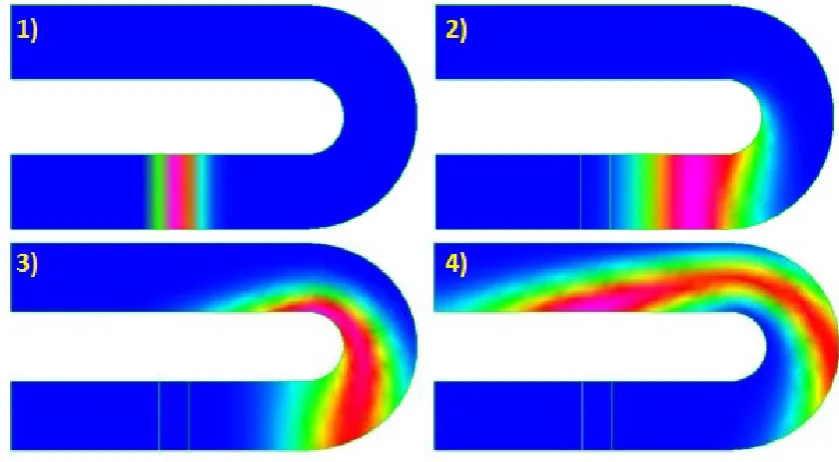
Design aspects
The chosen design is a 1 cm long straight column with a width of 300µm. This shape is chosen in order to eliminate the racetrack effect. Here, band distortion is caused by the fact that the inner portion of a liquid plug is travelling less distance in a turn than the outer portion of the plug. This effect skews the bands, resulting in a more diluted profile in the shape of a parallelogram. These parallelograms eventually form a rectangular shape again due to the collapse of the parallelogram by radial diffusion. This is an additional efficiency loss[175]. A visual representation of this distortion in the concentration is
shown in figure 2.1. A more detailed study of this effect and the resulting dispersion model can be found in the paper of Baidyaet al.[176].
Figure 2.1: Simulated racetrack effect. Picture taken from reference 177.
Master’s thesis
The chip with 3 inlets has an additional inlet for the oil. The working principle of the chip with 3 inlets is shown schematically in figure 2.3. The chip with 2 inlets works almost the same. This one does not have the oil inlet.
(a) Chip design with two inlets. (b) Chip design with three inlets.
Figure 2.2: Chip designs with two and three inlets.
Figure 2.3: Schematic representation of the working principle of the designed chip.
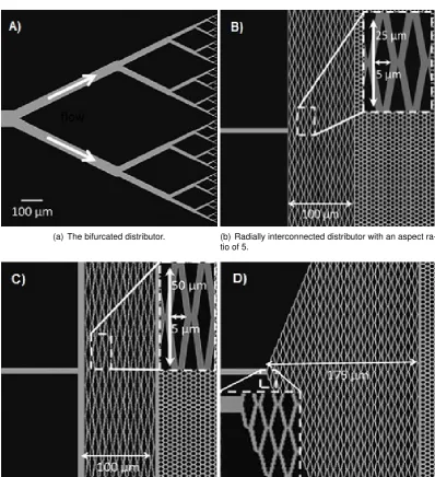
The column is much wider than the inlet channels, as can be seen in the pictures of figure 2.2. The entrance channel before the column and the exit channel after the column have a width of 50µm. The column itself has a width of 300µm. This gives a problem with the transition from entrance channel to column. The increase in width disturbs the profile of the liquid, which is really disadvantageous when the DNA needs to be eluted in a plug. The plug will form a parabolic profile as soon as the plug leaves the entrance channel[178]. In order to solve this problem, bifurcating channels are designed[179]. Such
a channel is shown in figure 2.4(a). As is visible, the channel divides every time in two new channels and with every separation, the width is divided by 2 in order to maintain a constant flow velocity. The total amount of inlets into the column is 2n, wherenis the amount of separation generations, which is
6 in figure 2.4(a). However, it is proven that these kind of flow distributors do not work optimal. The resulting band of the plug is not completely smooth, having rounded edges and the band volume is also relatively large, meaning longitudinal diffusion[180,181]. This is all due to the large volumes of the channels[178]. Another drawback of the bifurcating channels is their sensitivity to local etch errors or obstructions. When one of the channels is obstructed, the flow resistance will change locally, making that the liquid at that point cannot mix with the liquid in the other channels and therefore it will leave the distributor at a different time than the rest of the liquid[180,181].
Vangeloovenet al. designed therefore a radially interconnected flow distributor with better perfor-mances[181]. Such a flow distributor is also shown in figure 2.4. The band profile of these kind of distributors are proven to be more straight, without rounded edge and they are less sensitive to local etch error or obstructions since all channels are interconnected with each other. Vangelooven et al.
investigated different aspect ratios and found that an aspect ratio of 15 (axial width of 5 µm and a transversal length of 75µm) is the best choice for a design with single distributor region[181]. Such flow
distributor will be implemented before and after the column.
Master’s thesis
(a) Column design with square pillars.
(b) Column design with round pillars.
(c) Column design with round and densely packed pillars.
Figure 2.5: Different column designs with square, round, and round and densely packed pillars.
APTES and chitosan. Both molecules are already described in chapter 1 and literature has proven that both functionalizations are suitable for ion exchangeµSPE. The protocol for the functionalization is given in chapter 3.
After functionalization with an amino-terminated SAM, the column is prepared by flushing it with a 2-(N-morpholino)ethanesulfonic acid (MES) buffer of pH 5. This buffer will protonate the amino end-groups. Then, DNA dissolved in the same buffer will be flown through the column. The DNA will bind electrostatically with the protonated amino groups. After binding, the channel is flushed with the MES buffer in order to remove any proteins and other contaminants and PCR inhibitors. The next step is the elution step. This will be performed with a tris(hydroxymethyl)methylamine hydrochloride (TRIS, pH 9) buffer plug in an oil stream. The volume of the plug will be determined on basis of the elution profile and is the smallest amount of buffer needed to elute a significant part of the extracted DNA. The operating principle is schematically represented in figure 2.3.
Master’s thesis
Figure 2.10: Schematic representation of the different surfactant classes, with A) non-ionic, B) anionic, C) cationic, and D) zwitterionic. Picture taken from reference 217.
spaces between the base pairs) easily and they do not need any PCR step to incorporate them into the structure. There is little known about the involved chemistry of intercalation[218], but the fact that they
can bind between every base pair makes them the most interesting dye for the quantitation of low DNA concentrations.
Figure 2.11: Schematic representation of the different fluorescent dyes available for DNA detection. Picture taken from reference 219.
However, in general it is quite difficult to measure low concentrations of DNA accurately with flu-orescence. Low concentrations of DNA do not show linear behaviour when measured with fluores-cence[174]. This nonlinear behaviour was recently again demonstrated by Bruijns in the Mesoscale
Chemical Systems research group of the MESA+ Institute for Nanotechnology. These results are not published, but a graph is kindly made available by Bruijns and shown in figure 2.12. The measurements are done on a Tecan Infinite 200 Pro microplate spectrophotometer with 1.0X Evagreen as fluorescent dye (100µL 2.0X EvaGreen and 100µL DNA solution). The extinction is done at 500 nm and the emis-sion is measured at 530 nm. This EvaGreen dye is, together with SYBR Green the most widely used fluorescent dye for DNA quantitation.
Master’s thesis
Figure 2.12: Low amounts of DNA measured with a Tecan Infinite 200 Pro spectrophotometer and 1.0X EvaGreen. Excitation is done at 500 nm and emission is measured at 530 nm.
The used detection method is the Qubit high sensitivity dsDNA assay kit with the Qubit fluorometer of Invitrogen. This especially formulated assay kit comes with ready-to-use dilution buffer solution, concentrated assay reagent solution with fluorescent dye (SYBR 32 in DMSO[220]), and pre-diluted
DNA solutions (one of 0 ng/µL and one of 10 ng/µL). The measurements are as easy as following the next steps (a complete protocol can be found in appendix D):
1. Dilute the reagent with the provided buffer;
2. Add the sample (any volume between 1 and 20µL); 3. Incubate for 2 minutes;
4. Measure the concentration with the Qubit fluorometer.
The most significant advantage of this set is its linearity and selectivity[219]. UV absorbance based
quantitation cannot be used for mixtures of DNA and RNA, where the Qubit assay can quantitate DNA and RNA separately in a mixture of both with the use of the Qubit DNA assay kit and Qubit RNA assay kit, respectively. This selectivity is shown in figure 2.13.
Figure 2.13: Performance of the Qubit dsDNA HS assay, showing its linearity in the range of 0.2-100 ng and selectivity for DNA, even in the presence of an equal mass of RNA. Picture taken from reference 221.
The Qubit HS dsDNA assay kit has a linear signal in the initial sample concentration range of 10 pgµL-1 to 100 ng µL-1. The Qubit fluorometer gives values in µg mL-1 or ng mL-1. This
Master’s thesis
sponds to the concentration after dilution of the sample into the assay tube. The initial concentration ([DN A]initial) in ng/mL can be calculated with equation (2.24). In this equation, theQF value is the
value given by the Qubit fluorometer andVpipetted is the number of microliters of sample added to the
assay tube.
[DN A]initial=QF value×
200
Vpipetted
(2.24) The assay kit tolerates common contaminants, like salts, free nucleotides, solvents, detergents, and proteins. The assay signal is also stable up to three hours[219]. These advantages increase the ease of
Chapter 3
Methodical
The chips are fabricated with different standard clean room techniques. The main steps are, in chrono-logical order, wet oxidation, photolithography, reactive ion etching of the silicon oxide, directional DRIE (BOSCH process) of silicon, anodic bonding, and dicing. Then, the channels are functionalized with an amino termination via chemical surface modifications. The chips are ready to be used for the extraction, once the functionalization step is done. The extraction of DNA is analysed with the previous described Qubit dsDNA HS assay kit of Invitrogen. In the following paragraphs, global information about each of these steps is given. More detailed information can be found in appendix C and appendix D.
3.1
Fabrication process overview
The process flow with the fabrication steps of the chips consists of several standard clean room steps. These steps are, in chronological order, wet oxidation, photolithography, reactive ion etching (RIE) of silicon oxide, directional BOSCH DRIE of silicon, anodic bonding, and dicing of the silicon/borofloat stack into individual chips. A global overview of these steps with a cross section of the chip is given below. The cross-sections are made with CorelDRAW X6 (Corel Corporation, Ottawa, ON, United States). A detailed process flow, with the used equipment and parameters can be found in appendix C. In the clean room, Q-BASF sulphuric acid (96% VLSI Selectipur) and hydrogen peroxide (31% VLSIn Selectipur) are used.
3.1.1
Front side processing
Selection of a<100>DSP Si DSP wafer
Standard cleaning
Wet oxidation
Master’s thesis
Photoresist spinning
Alignment Exposure
Development Quick dump rinsing Drying
RIE of SiO2
DRIE (BOSCH) of Si
Resist and primer stripping in O2plasma Piranha cleaning
Quick dump rinsing Drying
3.1.2
Backside processing
Dehydration bake Primer spinning
Photoresist spinning
Master’s thesis
Alignment Exposure
Development Quick dump rinsing Drying
Postbake
RIE of SiO2
DRIE (BOSCH) of Si
Resist and primer stripping in O2plasma Piranha cleaning
Quick dump rinsing Drying
Oxide stripping in 50% HF Quick dump rinsing Drying
3.1.3
Cover wafer processing
Selection of Borofloat BF33 500 µm glass wafer
Master’s thesis
Manually aligning Prebonding Anodic bonding Applying UV dicing foil Dicing
Flood exposure Removing dicing foil
3.2
Micro world to macro universe a.k.a. fluidic coupling
During functionalization and extraction the chip is placed in a home-made chip holder (see figure 3.1). This chip holder also made it possible to connect the chip to the macro world. For this Upchurch Scientific NanoPort (IDEX Health & Science, Oak Harbor, WA, United States) connectors and capil-laries of 50µm I.D. and 360µm O.D. from the Polymicro Technologies company (Phoenix, AZ, United States) are used. The capillaries are connected to the chip with F-123H polyether ether ketone (PEEK) fittings and N-123-03 perfluoroelastomer ferrules. The connection between the capillaries and syringes are made with P-662 Luer-to-MicroTight adapters. As mentioned before, the flow direction of the liq-uids in the chip is managed with off-chip valves. These valves are 1-way (EW-30600-00) and 4-way (EW-30600-04) male lock polycarbonate stopcocks from Cole-Parmer (Vernon Hills, IL, United States). The connection between the capillaries and the valves is made with P-656 Male Luer to 10-32 Female adapters, P-662 Luer-to-MicroTight adapters, and F-120X fingertight fittings (all of Upchurch Scientific).
Figure 3.1: Photograph of the used homemade chipholder with connections for capillaries.
3.3
Functionalization
Master’s thesis
3.5
Analysis method
The analysis of the extracted DNA is done with the Qubit dsDNA HS assay kit, the 500µL thin-walled polypropylene assay tubes, and the Qubit fluorometer of Invitrogen (Carlsbad, CA, United States), as mentioned in the previous chapter. This kit requires a sample volume of anything in between 1 and 20µL. This is filled to 200µL with the working solution, which is made by combining the reagent and buffer of the assay kit in a 1:200 ratio. The fluorometer is calibrated with the two standards of the assay kit and after doing this, the samples can be measured. The working principle of this fluorescence method is schematically depicted in the flowchart of figure 3.3.
Figure 3.3: Work flow of the Qubit dsDNA HS assay kit. Picture taken from references 224 and 225.
Chapter 4
Results and discussions
In the now following paragraphs, the results of this research are discussed. The results are divided into different sections. First of all the results of the COMSOL simulations are discussed in the paragraph about CFD results. Then, results of the fabrication process are discussed. During the whole fabrication process, different techniques are used in order to monitor and check the different steps. After the fabrication process comes the functionalization of the chip. Different test methods are used in order to determine the best approach, and the results of these tests are discussed in the third paragraph of this chapter. The fourth paragraph discusses the results of the extraction, which are obtained with the Qubit dsDNA HS assay kit.
4.1
Computational fluid dynamics
In order to determine the best geometry of the column, COMSOL Multiphysics 4.3b is used. With this FEM software package, CFD analysis can be performed. The first analysis that is done was the de-termination of a good pillar geometry and orientation. Different geometries, namely square and round pillars, and different orientations of the squares, namely with the flat side perpendicular to the flow and the corner directed towards the flow direction. Besides this, the placement of the pillars is also investi-gated. Some are placed in a line grid, while others are placed in a hexagonal grid. An overview of the simulated pillars is shown in figure 4.1. Results of these analyses are shown in appendix E. The pitch of the square micropillar array is chosen to be 28.28µm in both directions, the pitch of the round micropil-lars is 30µm in thex-direction and 20µm in they-direction, and the pitches of the denser packed array with round micropillars is 20µm in both directions. The hexagonal packed arrays have micropillars on the half of the pitches, and elevated by 45°. The pictures in figure 4.2 show the best results for the 3 different kind of pillar arrays. A flow rate of 1.0µL min-1is used for these simulations.
Figure 4.1: Overview of the different simulated pillar geometries. In these figures, the flow is going from the left to the right.
Master’s thesis
(a) Round pillars that are placed in a hexagonal grid.
(b) Denser packed round pillars that are placed in a hexagonal grid.
(c) Square pillars, corner directed to the flow and placed in a hexagonal grid.
Figure 4.2: Velocity profile in columns with different pillar geometries and placements. The simulations are performed with a flow rate of 1µL min-1. All values are in mm s-1.
sidewalls of the channels with a densely packed array of round micropillars (see figure 4.3(a)). There-fore there are also simulations done with structures integrated in the sidewall of the channel. These results are shown in figure 4.3.
Based on these simulation it is clearly visible that the following columns would give the best results with respect to the requirement of constant flow velocity in the transversal direction of the column:
• The column needs to have micropillars which are placed in a hexagonal grid.
• The column needs to have round pillars or square pillars with a corner directed to the flow direction. • The column needs to have structures integrated in the sidewalls.
In order to reduce the amount of simulations, the following simulation is only performed with a column that has a hexagonal packing of round pillars and structures integrated into the sidewalls. The pillars are packed in a dens manner. This simulation is done to investigate the effect of the chosen flow distributor[180–182]. The result of the simulation with a flow rate of 0.1 µL min-1 is shown in figure 4.4.
As can be seen here, the distributor distributes the flow with a relatively high flow rate in transversal direction.
Besides this simulation, there are also other simulations done. At first is the pressure distribution inside the channel simulated. The result of this simulation is shown in figure 4.5. In here, it is visible that the largest pressure build-up is near the start of the flow distributor. This is as expected, since a channel with a cross section of 50×25µm2is splitted into two channels of 2.5×25µm2. The next simulation is
Master’s thesis
(a) A column without sidewall structures. (b) A column with sidewall structures.
Figure 4.3: Velocity profile in columns without and with sidewall structures. The simulations are per-formed with a flow rate of 1µL min-1. All values are in mm s-1.
Figure 4.4: COMSOL simulation of the velocity profile in the flow distributor, performed with a flow rate of 0.1µL min-1. All values are in mm s-1.
of the cell Reynold’s number in the middle of the channel (figure 4.6). This is not completely the same as the Reynold’s number in equation (2.20). COMSOL uses equation (4.1) and as can be seen here, there is a length scale involved. COMSOL uses the average mesh size for this, so it is the “local Reynold’s number”. This gives values roughly an order of magnitude lower than calculated analytically in equation (2.20) (also taking into account that a flow rate of 0.1 µL min-1 is used for the simulation). However,
the simulation shows that there is still a laminar flow because the cell Reynold’s number is lower than unity. The final simulated value is the shear stress, which is viscosity times shear rate for Newtonian fluids (see figure 4.7). This simulation is done in order to check whether the DNA will survive the flow distributor. As can be seen in the scale bar, the highest shear stress is 3.22×10⁻²³N pm-1. Literature gives values of 6.3×10⁻²³N pm-1for breakage induced by hydrodynamic shear stress[226], so DNA has a significant chance to survive this. If breakage still occurs, then this is not a big problem, since the next step downstream is PCR amplification and PCR also works with DNA fragments[227].
Recell=
vL
Master’s thesis
Figure 4.5: COMSOL simulation of the pressure distribution inside the column, performed with a flow rate of 0.1µL min-1. All values are in bar.
Figure 4.6: COMSOL simulation of the cell Reynold’s number, performed with a flow rate of 0.1µL min-1.
Figure 4.7: COMSOL simulation of the shear stress, performed with a flow rate of 0.1µL min-1. All
values are in N pm-1.
Master’s thesis
(a) SEM image of the column inlet. (b) SEM image of the column outlet.
(c) SEM image of the straight square pillars. (d) SEM image of the design error.
(e) SEM image of an etch effect.
Figure 4.9: SEM analysis of theµSPE column with square pillars.
is schematically depicted in appendix G, is performed with an EVG EV501 anodic bonder (St. Florian am Inn, Austria). Literature described anodic bonding of structures as small as 10×10 µm[228], but
Master’s thesis
(a) At t = 0 s.
(b) At t = 1 s.
(c) At t = 2 s.
(d) At t = 3 s.
Figure 4.11: Fluid profile analysis of a liquid. The fluorescein is flushed away with DI water at a flow rate of 10µL min-1.
Figure 4.12: The strong transversal distribution in the flow distributor.
4.4
Functionalization
Functionalization of silicon with either chitosan or APTES is tested on 1.5×1.5 cm<100>Si samples, which are created by dicing a wafer. This is done in order to verify whether the functionalization process is effective or not. These samples are analysed with two distinct and well-established surface analysis methods. The first used method is X-ray photoelectron spectroscopy (XPS). This technique uses X-rays in order to extract Auger electrons from the atoms on the surface. These Auger electrons have distinct energy values for different elements. With this technique it is possible to measure the relative compo-sition of the surface. The XPS spectra for both the chitosan functionalization as well as the APTES functionalization are given in appendix I. A summary of the results for the chitosan functionalization can be found in table 4.1.
Master’s thesis
(a) Microscope image of an empty channel. (b) Microscope image of an oil filled channel.
Figure 4.13: Microscope images of velocity profile test with oil.
Table 4.1: XPS results chitosan functionalization. C[%] N[%] O[%] Si[%]
Piranha cleaned SiO2 12.38 - 46.96 40.66 (54% bare Si, 46% SiO2 GPTMS 14.16 0.86 46.97 38.01 (54% bare Si, 46% SiO2 Chitosan 26.22 2.11 42.88 28.79 (54% bare Si, 46% SiO2
same time as the samples for the GPTMS and chitosan functionalization. The time between cleaning and analysis is therefore 27 h. The increase of carbon after the GPTMS functionalization is due to the carbon atoms present in the carbon backbone of GPTMS (a total of six carbon atoms is present in the chain, as can be seen in figure 4.14). This additional carbon decreases the amount of silicon in the re-sults because the analysis depth of the XPS is limited[229]. This is also the reason why the percentage
of silicon further decreased after the chitosan functionalization. Chitosan is a mucopolysaccharide (see figure 1.15) and therefore contains relatively a large amount of carbon. This is evidenced by the per-centage of carbon measured. Also 2.11 % of nitrogen is measured, indicating the nitrogen of the amino groups. The 0.86% of nitrogen in the GPTMS layer is unexplainable. A guess is that it also is adsorbed from the air.
Figure 4.14: Structural formula of GPTMS.
Master’s thesis
(a)∼6.5 mm into the channel. (b)∼5.7 mm into the channel. (c) 0 mm into the channel.
Figure 4.16: Microscope images taken after 20 minutes of applying a vacuum.
point, the pressure drop became too high and the Bernoulli pump came off from the water faucet (see figure 4.17. As can be seen in the microscope images in figure 4.18, the water continued to advance via the sidewalls of the channel until it reached the second distributor.
Figure 4.17: Bernoulli pump faillure due to a too high pressure drop.
(a) 10 mm into the channel. (b)∼6.0 mm into the channel.
Figure 4.18: Microscope images taken after 35 minutes of applying a vacuum.
Master’s thesis
Figure 4.20: The home-made setup to get piranha into the chip.
Figure 4.21: The occurred leakage next to the inlet plug.
Master’s thesis
However, it is assumed that there are some active hydroxyl groups on the channel walls and pillars. The functionalization is performed by flushing a 4% v/v APTES solution in ethanol into the channel. Once the channel was filled, the flow was stopped. Fresh APTES solution was flushed with a flow rate of 1µL min-1 into the channel after it reacted for 2.5 h. This fresh solution also stayed inside the
channel for 2.5 h. Afterwards, the channel was flushed with ethanol and the MES buffer that is used to protonate the amino groups. Then, a DNA solution was flown through the chip. However, this was not successful because the channels became clogged. In an attempt to solve it, all solutions were filtered with a Nuclepore polyethylene filter with 2.0µm pore size (Pleasanton, CA, United States). This filter membrane was placed directly on top of the chip and the connections are made with the membrane in between the chip and the outlet of the capillary. However, this method was not successful, as can be seen in figure 4.22. This can be an accumulation of dirt with dimensions smaller than 2.0µm, which eventually blocked a channel of 2.5µm width. A possible way of solving this is by filtrating the solution with a 0.45 µm syringe filter disk prior to injecting it into the channel. However, this is not a desired method because the filtrating can also capture some of the DNA, and this is not wished with forensic samples, which are low in DNA concentration.
Master’s thesis
2 and 40% difference with the standard concentration of 10 ngµL-1, the method is still used throughout
this research, since the method has proven to be more useful than conventional fluorescence measure-ments. The supplier guarantees linearity between 0 and 100 ngµL-1 if every sample is measured with
the same standards. The straightforwardness of the analysis method simplifies the method significantly and increases the throughput of samples.
5.5
Extraction
The extraction of DNA was only performed on flat test samples since the functionalization of the chip was not achieved. The results of the extraction and elution tests with the different functionalizations does not give a conclusion which functionalization is the best. For the extraction of DNA from the MES buffer, a APTES monolayer which is grown in dry toluene extracts the most of the DNA, namely almost 95%. However, the elution of this same sample was only∼4.2%. For this elution step a TRIS buffer of pH 12.6 was used. The elution efficiency with this buffer was already better than the elution from APTES with a TRIS buffer of 9.2, only a mere 0.1% was eluted. Chitosan on the other hand, had a low extraction efficiency. This was only∼10.5%. However, the elution efficiency was rather high when compared to the elution efficiencies of the APTES layers, namely∼18.8%. These differences in extraction efficiencies can be explained by the functionalization steps, which were, according to the XPS and contact angle measurements results, done at non-optimal reaction conditions. The time did not allow it to further investigate the different parameters of the functionalization steps. The low elution efficiency of the APTES can possibly be explained with the pKavalue of APTES. The literature describe a whole range
of different values[116–119], making it difficult to find a proper buffer solution. The only conclusion that can
be made here is that the reproducibility between test samples with the same functionalization is high, which is proven by the low experimental error (standard deviation).
5.6
Overall conclusion
The chosen method of ion exchangeµSPE is a potential interesting method for DNA extraction. How-ever, the chosen functionalization and buffer combinations did not yield the desired combination of a high extraction efficiency and high elution efficiency. Further research can give more clarity in which combination needs to be chosen in order to have the optimal combination. The chip design itself was also not optimal for the extraction of DNA. The column itself was not the problem, but the distributor gave the problems. The chosen distributor has channels of 2.5µm wide and the depth of the distribu-tor was quite large, when compared to the width, making it prone for clogging. Equation (2.17) learns us that the created pressure drop is related to the viscosity of the fluid. The fact that oil has a higher viscosity, together with the channel dimensions, make it that the oil could not enter the distributor. All recommendations for further research can be found in chapter 6.
Master’s thesis
aminomethylphosphonic acid (AMPA). This molecule needs less cross-linking during the SAM for-mation. This molecule is used quite a lot as a stationary phase in the chromatography world[244],
so its chemistry on silica is well-established.
Figure 6.1: A corona discharge plasma arc travels freely from the inlet to the outlet via the unblocked outer channel. Picture taken from reference 240.
Besides these recommendation, there are also some for the characterization of the chip:
• Until now, there is only looked at the reproducibility between different chips. It can also be useful to look at the inter-chip reproducibility, i.e. performing multiple extractions with the same chip. With this test, the durability of the functionalization can be tested.
• Also the elution profile of the chips need to be measured. This method is already described before, but there was no functional chip produced during this research. Therefore it is still a recommendation for further research.
6.2
Integration
Once this system is designed in such manner that both the extraction and the elution efficiency are as high as possible, it can be integrated into a forensic LoC device. Such a system can have a sequence that starts with the input. The input can be a collected sample from the crime scene. This sample can be lysed, but the lysis can also be done on chip[245]. The sample then arrives at theµSPE part. Here, all the DNA is extracted from the sample solution, removing all contamination and amplification inhibitors. From here on, the sample is eluted to a flow focussing emulsifier[204,205]. This divides the DNA over a
stream of multiple droplets in an oil or air. The stream of droplets goes to the amplification part of the chip. The method which can have a high specificity for human DNA is PCR amplification[227]. There
are severalAlusequences present in human DNA[246–248]and these can be amplified if the primers are
chosen in a proper way. This amplified DNA is mixed with a fluorescent dye and the final mixture can be measured with on-chip fluorescence measurements with a led and a Si photodiode[249].
Figure 6.2: Design for fluorescence detection on chip. Picture taken from reference 249.
Master’s thesis
[288] Hampton Research. Optimize, certificate of analysis, titration table for 0.5 M MES with 1.0 M sodium hydroxide, . URL http://hamptonresearch.com/documents/product/ 0000000132-0000000269.pdf.
[289] Hampton Research. Optimize, certificate of analysis, titration table for 1.0 M Tris HCl with 1.0 M sodium hydroxide, . URL https://hamptonresearch.com/documents/product/ 0000000137-0000000284.pdf.
Aknowledgements
Nu dat dit master scriptie onderzoek ten einde is, wordt het tijd om wat mensen te bedanken. Allereerst wil ik prof. Han Gardeniers en Roald Tiggelaar bedanken. Via Han heb ik deze opdracht gekregen, waarbij Roald mijn dagelijkse begeleider werd. Roald, heel erg bedankt voor je geduld en je hulp met het corrigeren van mijn scriptie.
Ook wil ik graag mijn medekantoorbewoners, Hoon Suk Rho, Mattia Morassutto, en Peter van der Linde. Peter kende ik al van de opleiding, en ik zal onze koffiemomentjes missen. Hoon, I will never forget your dedication to PDMS and how you wanted that I would work with PDMS as well. I also will never forget your other dedication: Molly Malone. It was really fun going there with you all! Mattia, I am still hearing you cursing in Italian from behind your computer screen: Vaffanculo!! Cazzo!! And of course I woul like to thank all the people of MCS for the great time! I hope to see you all soon again!!
People from out of MCS which I would like to thank are Yoonsun Yang and Dani ¨el Hagedoorn. Yoon, thank you that I could use the Qubit fluorometer of the MCBP group!! Dani ¨el, bedankt voor je hulp bij de contacthoekmetingen die ik bij de PCF groep kon doen! Verder wil ik graag de hele clean room staff bedanken voor hun trainingen en hulp tijden mijn fabricage proces.
Als laatste wil ik graag mijn ouders, broertje, en mijn vriendin Linda bedanken voor hun steun en geduld! Het lijkt mij maar moeilijk om met zo’n rare nanotechnoloog opgescheept te zitten.
Appendix A
Microfabrication steps
The idea of theµSPE chip is already explained in chapter 1. In order to fabricate such a chip, some dif-ferent fabrication steps are performed. These steps, in order of execution on a silicon<100>DSP wafer, are standard cleaning, wet oxidation, front side photolithography, deep reactive ion etching (BOSCH pro-cess), cleaning, backside photolithography, BOSCH process on the backside of the wafer for the holes, and cleaning. Then, a glass borofloat wafer is cleaned and anodic bonded on the silicon wafer, followed by dicing the wafer into separate chips. The final step is the channel functionalization with chitosan or 3-aminopropylsilane. In the now following paragraphs, some attention is paid to the most important fabrication steps,i.e. wet oxidation, photolithography, deep reactive ion etching (BOSCH process), an-odic bonding, channel functionalization, and the coupling of the micro world to the macro world. The cleaning steps are not further discussed here. The whole process flow can be found in appendix C.
A.1
Thermal oxidation
Thermal oxidation of silicon gives silicon dioxide. This material is amorphous and not the same as crystalline quarts (SiO4) because bonds are not perfectly formed at the silicon/oxide interface, leaving atoms unbound and charged[251]. The structure of the silicon/oxide interface is shown in figure A.1.
Figure A.1: The crystalline silicon and amorphous oxide interface. Dangling bonds are visible on atoms that do not have their full valence and some have hydrogen atoms bonded to them. Picture taken from reference 251.
There are two basic methods for the thermal oxidation of Si: wet and dry oxidation. The wet thermal oxidation has water gas and dry oxidation oxygen gas present in the oxidation furnace. The represen-tative chemical reactions are shown in reaction 1 and 2, respectively.
Si(s)+2 H2O(g)−−→SiO2(s)+2 H2(g)
Si(s)+O2(g)−−→SiO2(s)
Master’s thesis
Figure A.7: Schematic representation of a basic two step Bosch process, which starts with (A) an etching step and is followed by (B) an passivation step. Picture taken and modified from 251.
good balance is found, aspect ratio’s as high as 40[261], or more recently even 97[262]can be achieved
with the BOSCH process. The complex interdependence of some general DRIE parameters and etch responses on the wafer is shown in figure A.8.
Figure A.8: The complex interdependence of some general DRIE parameters and etch responses on the wafer. Picture taken from reference 251.
A.4
Anodic bonding
Anodic bonding is also known as field-assisted thermal bonding (FATB) and is a direct bonding tech-nique to mate two complete wafers, a silicon and glass wafer, and is used to hermetically seal and encapsulate the final structures in silicon[263–265]. The technique is the oldest bonding technique in
microfabrication[263] and is based on bonding via elevated temperatures (usually in the range
200-500°C[263,266]) and voltages (usually in the range 100-1,000 V[263,266]). Glass will conform at
tempera-tures of 400-500°C, which will seal structempera-tures and irregularities of up to 50-60 nm hermetically[263,265].
At a temperature of 400°C, sodium oxide (NaO2) will decompose into sodium and oxygen ions, 2 Na+ and O2–, respectively[263]. The bonding process uses a voltage between 100-1,000 V, which is applied
to the glass wafer[263,266]. The sodium ions become mobile at the elevated temperatures and start to
migrate towards the glass top surface (cathode) because of the applied voltage. This leaves the rela-tively immobile oxygen ions behind at the glass-silicon interface[266]. This accumulation of oxygen ions
will form a depletion layer (or space charge region). Then, an equivalent charge of opposite sign will form on the silicon side of the glass-silicon interface. This region is called the image charge[266]. Now, an electrostatic force will pull the glass and silicon wafer together[263] and the charged regions result in a high electric field across the glass-silicon interface[266]. This electric field has a magnitude up to
106V cm-2 [267]. The oxygen ions are drifted away from the sodium depletion region to the glass-silicon
interface[266]. Here, they will react with the silicon, leading to irreversible chemical SiO
2bonds
(oxida-tion)[266,268]:
Master’s thesis Si+2 O2–−−→SiO2+4 e–
The sodium ions are neutralized at the cathode. The elevated temperatures will cause that more ionization will take place, but also that the diffusion of ions is faster, so the depletion width is greater, leading to stronger bonds[263]. The diffusion is mainly dependent on the applied voltage[266]. A small
voltage causes that the drift velocity and kinetic energy of the oxygen ions cannot sustain a high oxida-tion rate at the bonding front. This leads to longer bonding times, or even non-bonded substrates. This charge (re)distribution process is shown in figure A.9 and the applied voltage-bonding time relation is shown in figure A.10. This makes the magnitudes of applied DC voltage and temperature, the bonding time, and surface characteristics the most deterministic parameters for the anodic bonding process[269].
Figure A.9: Schematic representation of anodic silicon-glass bonding, illustrating the charge distribution during bonding. Picture taken from reference 266.
Figure A.10: Plot of bonding time versus applied voltage for a p-type silicon wafer and Corning 7740 glass wafer. Both substrates were pre-cleaned using acetone. Picture taken from reference 266.
The bonding mechanism can be initiated by simply applying some pressure at the centre of the wafer. This can be omitted when the bonding is performed in a vacuum[263]. The size of bondable area
can be small. Silicon pillars of 10µm diameter have been bonded to glass, as described by de Malsche
et al.[228].
A.5
Channel functionalization
The functionalization of the channel and pillars is based on conventional silicon oxide surface chemistry via self-assembled monolayers (SAM). A SAM is only a couple of nanometres thick, but it can completely change the properties of a surface. The use of self-assembly is already known since 1946, when Zis-manet al. used monolayers of long-chain hydrocarbons with polar head groups on polar surfaces[270].
Even though these layers were extremely thin (roughly 2 nm), they were able to change the surface properties completely. The first real application for SAMs came a little bit more than three decades later, when Polymeropouloset al. used it for measuring electrical conduction between two metal sur-faces[271]. The real revolution started when Sagiv published the results of his work on organosilane
monolayers on SiO2[131].
Master’s thesis
can be done via, for example, metal complex catalysed hydrosilylation[272,273], or radical-induced
hydro-silylation[274–276]. The hydrosilation method is an unsuitable method for silicon with a (native) oxide layer
because this needs an hydrogen-terminated surface in order to attach a SAM via, for example, This hydrogen-terminated surface is created by etching away the (native) oxide in HF[277]and this makes it
a unsuitable method for coating a silicon oxide surface. In order to attach a monolayer to a silicon oxide surface, silanization of the (native) silicon oxide layer via a liquid phase[138,278–280]or gas phase[281–283]
can be performed. The gas phase silanization reactions can be performed via heating up the silane reagent[281], gas formation in a vacuum chamber[282], or vacuum distillation[283]. The main problems of
the gas phase method is that it results in a layer with high variations in silane amounts and quality of the layer[284], that it takes up to several hours before the reaction is finished[284], and that it requires more advanced equipment.
The silanization process consists of two steps,e.g.the hydrolysis of the leaving groups (for example alkoxy groups) and the condensation of surface silanols with the silanols of the silane molecule[131,284]
in an anti-Markovnikov fashion[274]. Studies have shown that these two steps occur when the silane
molecules come in contact with the adsorbed water layer on the (native) silicon oxide surface[285,286].
A monolayer of water is promoting the coverage and quality of the SAM formation[131]. Vacuum fired
samples show a saturation coverage for octadecyltrichlorosilane which is roughly three times smaller than the saturation coverage on a surface of hydrated silicon oxide[285]. More information about SAMs
and organometallic surface chemistry on silicon can be found in the comprehensive reviews written by Onclin, Ravoo, and Reinhoudtet al.[?] and Buriak[273]. This water promoted functionalization makes
a liquid phase functionalization favourable in this study. In order to increase the quality of the formed layer even further, the silicon oxide is activated with piranha solution (1:3 v/v 30% H2O2/96% H2SO4). This reagent removes any organic contamination and creates hydroxyl groups[287]. This is useful since
native oxide has a low surface hydroxyl (−OH) group content[285].
Appendix B
Photolithography masks
(a) Mask with channels for frontside lithography.
(b) Mask with via-holes for backside lithography.
Appendix D
Protocols
D.1
Chelex DNA isolation
1. Rinse your mouth for 10 s with 0.9% NaCl. 2. Spit the mouthwash into a plastic cup.
3. Transfer the mouthwash into a centrifuge tube and close the lid. 4. Centrifuge for 10 minutes at 500∼1,000 g.
5. Transfer the supernatant into the plastic cup, while keeping the cell pellet intact. 6. Put the tube with the cell pellet on ice.
7. Add 500µL 10% Chelex solution to the cell pellet (mix the Chelex suspension a couple of times in order to get a homogeneous solution before adding it to the cell pellet).
8. Resuspend the cells in the Chelex solution by pipetting it a couple of times.
9. Pipet 500µL of the resuspended solution into a 1.5 mL Eppendorf cup and close the lid. 10. Puncture the lid of the Eppendorf cup.
11. Heat the cup for 10 minutes at 100°C. 12. Cool the cup for 1 minute on ice.
13. Centrifuge the cup for 30 s on maximal rpm in order to filtrate the Chelex grains.
14. Pipet 200µL of the supernatant (leave the Chelex pellet behind) into a new 1.5 mL Eppendorf cup en freeze it.
D.2
Buffer preparation
The buffers are prepared according to tables of Hampton Research. The buffers are made according following protocols:
MES buffer of pH 5.0[288]:
1. Add 510µL 1.0 M NaOH solution in 100 mL glassware. 2. Add 20 mL 0.5 M MES solution to it.
3. Fill it to 100 mL with DI water.
TRIS buffer of pH 9.2[289]:
1. Add 9.2 mL 1.0 M NaOH solution in 100 mL glassware. 2. Add 10 mL 1.0 M TRIS solution to it.
Master’s thesis
The TRIS buffer of pH 12.6[289]:
1. Add 18.54 mL 1.0 M NaOH solution in 100 mL glassware. 2. Add 10 mL 1.0 M TRIS solution to it.
3. Fill it to 100 mL with DI water.
The result of the first two buffers is tested with universal pH indicator paper and with a Mettler Toledo SevenMulti with an InLab Expert PRO pH probe (Greifensee, Switzerland). These results are shown in figure D.1 and table D.1.
Figure D.1: pH analysis with universal pH indicator paper.
Table D.1: Results of pH measurements with the Mettler Toledo SevenMulti with an InLab Expert PRO pH probe.
Buffer Measured pH
MES 5.01±0.02 (n=3)
TRIS buffer 1 9.23±0.08 (n=3)
TRIS buffer 2 12.61±0.02 (n=3)
D.3
Qubit dsDNA HS assay
1. Prepare working solution
• 200 µL is required for each sample and standard
• Dilute the reagent 1:200 in buffer, use a disposable plastic container 2. Make standards
• Add 10 µL of standard and 190 µL of working solution in a 500 µL PCR tube • Vortex 2-3 s
• Incubate for 2 min at R.T. 3. Prepare samples
Master’s thesis • Vortex 2-3 s
• Incubate for 2 min at R.T. 4. Measurement
• Turn on the Qubit fluorometer and press any button • Select assay to be performed
• Calibrate
Load first standard and press go Load second standard and press go • Read samples
Load sample tube 1 and press go Continue
Calculate starting concentration, using “calculate sample concentration” or manually calcu-late based on dilution in working solution
Appendix E
Computational fluid dynamics results
The simulations are done with the creeping flow physics package of COMSOL Multiphysics 4.3b (Burling-ton, MA, United States). As model liquid, water at room temperature is taken. No-slip boundary condi-tions are assumed because of the microfluidics regime. The column is 300µm wide and the pillars are either 10×10µm2or 10µm in diameter. All values of the scale bar are in mm s-1.
Figure E.1: Velocity profile in a column with square pillars with the flat directed to the flow and placed in a line grid.
Master’s thesis
Figure E.3: Velocity profile in a column with square pillars with the corner directed to the flow and placed in a line grid.
Figure E.4: Velocity profile in a column with square pillars with the corner directed to the flow and placed out of phase.
Figure E.5: Velocity profile in a column with round pillars that are placed in a line grid.
Master’s thesis
Figure E.6: Velocity profile in a column with round pillars that are placed in a hexagonal grid.
Master’s thesis
Figure E.8: Velocity profile in a column with sidewall structures and round pillars that are placed in a hexagonal grid.
Figure E.9: Velocity profile in a column with sidewall structures and denser packed round pillars that are placed in a hexagonal grid.
Appendix F
Microscope images of the
photolithography mask “
µ
SPE flow
channel”
Images are made with normal optical microscopy.
(a) Inlet of the column.
(b) Outlet of the column.
Master’s thesis
(a) Inlet of the column.
(b) Outlet of the column.
Figure F.2: Microscope images of the mask for the chip with a column with round pillars.
Master’s thesis
(a) Inlet of the column.
(b) Design error.
(c) Outlet of the column.
Appendix G
Fabrication related results
The results of several fabrication steps are combined in this appendix.
Figure G.1: Ellipsometry results of the wet oxidized Si made with a full wafer scan.
Figure G.2: Channel profile as measured with the Veeco Dektak profiler.
The small dip (making the maximal depth 24.07µm) in figure G.2, in the middle of the etched channel is due to the used BOSCH recipe (B-HARS)[180]. The sloped sidewalls are due to the stylus radius and
Master’s thesis
Figure G.3: Anodic bonding recipe.
![Figure 1.2: The amount of publications per year on A) microfluidics, B) micro total analysis system, andC) lab on a chip, lab-on-a-chip, lab on chip, lab-on-chip found in the renowned databases of Elsevier’sScopus[6] and Thomson Reuters’ Web of Science[7].](https://thumb-us.123doks.com/thumbv2/123dok_us/1052651.1131620/24.595.80.503.33.617/publications-microuidics-renowned-databases-elsevier-thomson-reuters-science.webp)