Thesis presented in partial fulfillment
of the requirements for the Degree of
Ph.D. in Computing
Logic Decomposition and Adaptive Clocking for the
Optimization of Digital Circuits
Lucas Machado
Advisor: Jordi Cortadella Fortuny
Computer Science Department
Universitat Politècnica de Catalunya
Abstract
Over the course of 60 years, since the invention of the integrated circuit (IC), exponential improvements in cost, performance and power consumption were observed. Such advances have been strongly linked with the continuous reduction of the dimensions in manufactured ICs, but this trend has shown decreasing benefits as fundamental limits are reached.
Notice that such tiny devices have increased variability, which generates unpredictable variations in the behavior of the manufactured devices. These uncertainties are typically addressed by defining margins on the clock period, estimated during the design phase. However, the overly conservative margins produce significant degradations in performance.
Additionally, the evolution that enabled circuits with increasingly higher density of components, also resulted in an extremely complex IC design. At every step, electronic design automation (EDA) tools are challenged to handle this increasing complexity, requiring more powerful techniques to comply with the specification constraints within an affordable runtime.
This thesis investigates alternatives in order to improve power, perfor-mance, area, and cost, using established IC manufacturing technologies. Ad-vances in EDA are proposed in three distinct topics: area minimization us-ing Boolean methods, area and delay reduction for designs based on field-programmable gate array (FPGA), and an alternative clocking scheme to reduce timing margins.
The first contribution consists of a technology-independent method for area minimization of combinational logic. Local optimization is applied on and-inverter graphs (AIGs), performing multi-output Boolean decomposition using two-literal divisors, targeting node count reduction.
The second contribution regards two methods targeting technology map-ping of FPGAs. On one hand, a functional decomposition approach, which uses the support size as cost function, exploring the inherent characteristics of FPGAs. On the other hand, an approach for recursive remapping, which reduces the structural bias of the subject graph, uses the mapping results as cost function, and obtains significant reductions in area and delay.
scheme based on ring oscillator clocks (ROCs). The impact of the PDN pa-rameters and ROC location is investigated, showing potential improvements in performance, leakage power and cost.
The contributions of this thesis have been published in the following papers:
• Lucas Machado, Antoni Roca, Jordi Cortadella. Increasing the Robust-ness of Digital Circuits with Ring Oscillator Clocks. InProceedings of the International Workshop on Resiliency in Embedded Electronic Sys-tems (REES), pages 29-34, March 2017.
• Lucas Machado, Jordi Cortadella. Boolean Decomposition for AIG Optimization. InProceedings of ACM Great Lakes Symposium on VLSI
(GLSVLSI), pages 143-148, May 2017.
• Lucas Machado, Antoni Roca, Jordi Cortadella. Voltage Noise Analysis with Ring Oscillator Clocks. InProceedings of IEEE Computer Society Annual Symposium on VLSI (ISVLSI), pages 1-6, July 2017.
• Lucas Machado, Jordi Cortadella. Support-Reducing Functional De-composition for FPGA Technology Mapping. In Proceedings of Inter-national Workshop on Logic & Synthesis (IWLS), pages 79-86, 2018.
Also, extensions of the published papers have been submitted to journals:
• Lucas Machado, Jordi Cortadella. Support-Reducing Decomposition for FPGA Mapping. In IEEE Transactions on Computer-Aided De-sign of Integrated Circuits and Systems (TCAD), 2018 (Accepted for publication).
• Lucas Machado, Antoni Roca, Jordi Cortadella. Robustness to Voltage Noise with Ring Oscillator Clocks. InIEEE Transactions on Nanotech-nology (TNANO), 2018 (Under review).
Acknowledgments
I would like to express my sincere gratitude to my advisor Prof. Jordi Cor-tadella Fortuny for giving me the possibility of pursuing my PhD degree in Barcelona. His guidance, motivation, strive for excellence, and unending source of ideas helped me a lot during every piece of work we did together. It was an incredible opportunity to work with him.
I also thank the advisors of my Master’s thesis in Brazil, André Reis and Renato Ribas, as they both encouraged me in thriving for a PhD degree in Europe. Especially André, for the connection between me and Jordi, and the support during the scholarship proposal and the first year in Catalonia.
I thank every person that I had the opportunity to work side by side these years in Barcelona. My lab colleagues Àlex Vidal, Alberto Moreno, Javier de San Pedro, Tuomas Hakoniemi, and Josep Sanchez, and the ones I had the pleasure to work with, Antoni Roca and Mayler Martins.
I also thank all my friends and family from Lajeado, Cachoeira do Sul, Porto Alegre, and now spread around the globe. You all helped me be who I am today, and certainly have a part in this degree. Particularly, my grand-parents (in memoriam to my grandma Maria, who passed away in this pe-riod), my father Carson, my mother Gisele and my brother Jonas. I certainly missed you a lot during these years, separated by 9642 km and several hours by plane. You were, are and will always be my support to everything, the giants that took me in their shoulders and made me look further.
For my wife Rafaela Bortolini, I may not have enough words to express my gratitude. For marrying me, embarking with me in such a life-changing adventure, getting way out of our comfort zones. For the understanding, loving and caring. For insisting on having a dog, our beloved Pipoca, that helped us so much with her partnership and joy. For everything, I thank you. This thesis has been performed with the support of CNPq, Conselho Na-cional de Desenvolvimento Científico e Tecnológico - Brasil, and has been par-tially supported by funds from the Spanish Ministry for Economy and Com-petitiveness and the European Union (FEDER funds) under grant TIN2017-86727-C2-1-R, and the Generalitat de Catalunya (2017 SGR 786).
Contents
Abstract iii Acknowledgments v Contents vii List of Acronyms xi List of Figures xvList of Tables xix
1 Introduction 1
1.1 Research motivation and goal . . . 4
1.2 Contributions of this thesis . . . 5
1.2.1 Boolean decomposition using two-literal divisors . . . . 5
1.2.2 Support-reducing logic decomposition and remapping . 6 1.2.3 Voltage noise mitigation using ROCs . . . 7
1.3 Manuscript organization . . . 8
2 Background 11 2.1 Logic synthesis . . . 11
2.1.1 Boolean functions . . . 11
2.1.2 Representation of Boolean functions . . . 13
2.1.3 Logic decomposition . . . 17
2.1.4 Local optimization . . . 20
2.1.5 Collapsing . . . 23
2.1.6 AIG transformations . . . 24
2.1.7 FPGA technology mapping . . . 26
2.2 Adaptive clocking . . . 28
2.2.1 Power Integrity . . . 28
2.2.2 Voltage noise . . . 29 vii
3 AIG Optimization via Boolean Decomposition 35
3.1 Motivation . . . 35
3.2 Overview . . . 37
3.2.1 Multi-output Boolean decomposition . . . 38
3.2.2 AIG optimization example . . . 38
3.2.3 Results obtained via AIG transformations . . . 39
3.3 AIG optimization approach . . . 41
3.3.1 Local optimization using KL-cuts . . . 41
3.3.2 Boolean decomposition . . . 42
3.3.3 Filters to reduce runtime . . . 44
3.4 Experimental results . . . 45
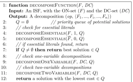
4 Support-reducing Decomposition for FPGA Mapping 49 4.1 Motivation . . . 49 4.2 Motivating Example . . . 52 4.3 Support-reducing decomposition . . . 54 4.3.1 Cost function . . . 55 4.3.2 Essential literals . . . 57 4.3.3 One-variable decompositions . . . 58 4.3.4 Two-variable decompositions . . . 59 4.3.5 Abstraction-based bi-decompositions . . . 60 4.4 Recursive remapping . . . 61 4.5 Experimental results . . . 64
4.5.1 BDD-based FPGA mapping tools . . . 65
4.5.2 20 largest MCNC benchmarks . . . 67
4.5.3 EPFL benchmarks . . . 70
4.5.4 Remapping of the results from a commercial tool . . . 71
4.5.5 SR-map result as input to the commercial tool . . . 73
4.5.6 Scalability analysis . . . 74
5 Robustness to Voltage Noise with Ring Oscillator Clocks 81 5.1 Motivation . . . 81
5.2 Models and metrics . . . 83
5.2.1 PDN model . . . 83
5.2.2 Delay model . . . 85
5.2.3 Performance Metric . . . 85
5.3 Voltage locality analysis . . . 88
5.3.1 Typical voltage noise . . . 89
5.3.2 Worst-case voltage noise . . . 90 viii
5.4.1 On-chip decoupling capacitance . . . 92
5.4.2 Power interconnections . . . 95
5.4.3 Package decoupling capacitance parasitics . . . 98
5.5 Discussion . . . 100
5.5.1 Simpler voltage/frequency scaling . . . 101
5.5.2 EMI reduction . . . 101
5.5.3 Benefits of multiple ROC domains . . . 103
5.5.4 Disadvantages . . . 103
6 Conclusions and Future Work 105 6.1 Summary of the thesis contributions . . . 105
6.2 Future work . . . 106
Bibliography 109
List of Acronyms
AI artificial intelligence
AIG and-inverter graph
API application programming interface
ASIC application specific integrated circuit
BDD binary decision diagram
BLIF Berkeley logic interchange format
CAD computer-aided design
CDC cross-domain crossing
CEC combinational equivalence checking
CMOS complementary metal-oxide-semiconductor
CP critical path
CTS clock tree synthesis
CUDD Colorado University Decision Diagram
DAG directed acyclic graph
DC don’t care
DDR double data rate
DRC design rule checking
DSD disjoint-support decomposition
DVFS dynamic voltage and frequency scaling
EDA electronic design automation
EMI electromagnetic interference
EPFL École Polytechnique Fédérale de Lausanne
ESL equivalent series inductance
ESR equivalent series resistance
FPGA field-programmable gate array
HDL hardware description language
HLS high-level synthesis
IC integrated circuit
IoT internet of things
ISF incompletely specified function
ITC International Test Conference
ITRS international technology roadmap for semi-conductors
LUT look-up table
MCNC Microelectronics Center of North Carolina
MFFC maximum fanout-free cone
PCB printed circuit board
PDN power delivery network
PI primary input
PLL phase-locked loop
PO primary output
POS product-of-sums
PPAC power, performance, area, and cost
PVT process, voltage, temperature
QoR quality of results
ROBDD reduced-ordered BDD
ROC ring oscillator clock
RTL register-transfer level
SDC satisfiability don’t care
SEC sequential equivalence checking
SoC system-on-chip
SOP sum-of-products
SPICE Simulated Program with Integrated Circuits Emphasis
SR-map support-reducing remapping tool
STA static timing analysis
VLSI very-large-scale integration
VRM voltage regulator module
List of Figures
1.1 Evolution over time of the transistors density and the
mini-mum feature size (Source: [36]). . . 2
1.2 Logic synthesis in the standard cell flow of integrated circuits. 3 2.1 (a) BDD and (b) ROBDD of the function F1 from Table 2.1. . 16
2.2 Example of an AIG, with 15 nodes and 5 levels. . . 17
2.3 Examples of (a) disjoint, (b) strong, and (c) weak bi-decompositions. 18 2.4 Example of a 1×1 window on top of a DAG (Source: [83]). . 20
2.5 Example of a graph covering with K-cuts (Source: [20]). . . 22
2.6 Example of KL-cut computation. . . 23
2.7 Example of the collapsing process for a primary output. . . 24
2.8 Examples of AIG rewriting (Source: [84]). . . 25
2.9 Example of a tree-balancing transformation (Source: [81]). . . 26
2.10 Distribution of solutions for the benchmarkcordic(Source: [38]). 27 2.11 PDN model with off-chip and on-chip parasitics. . . 29
2.12 (a) The frequency response of a typical PDN, and (b) the voltage droops generated by a single current spike . . . 30
2.13 Voltage droops generated by periodical current differences at (a) low and (b) high impedance frequencies. . . 31
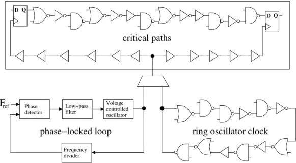
2.14 Synchronous circuit with a PLL or an ROC as the clock source. 32 2.15 PLL and ROC clock generation in the presence of voltage noise. 33 3.1 Decomposition using a two-literal Boolean divisor. . . 36
3.2 Iterative rewriting of KL-cuts on an AIG. . . 37
3.3 Optimization flow using different methods forb06. . . 39
3.4 AIG optimization using Boolean decomposition. . . 41
3.5 Boolean decomposition procedure. . . 43
3.6 Factored form trees fromb06 benchmark. . . 44
4.1 Correlation between the number of AIG nodes and LUTs after technology mapping (Source: [65]). . . 50
decomposition. . . 53
4.3 Pseudo-code of the proposed support-reducing decomposition. 56 4.4 Pseudo-code for an step of the support-reducing decomposition. 56 4.5 Pseudo-code for decomposition using essential literals. . . 57
4.6 Pseudo-code for one-variable decompositions. . . 58
4.7 Pseudo-code for two-variable decompositions. . . 59
4.8 The recursive remapping approach. . . 62
4.9 Pseudo-code of the recursive remapping approach. . . 63
4.10 Comparison of commercial tool results with the SR-map re-sult as input vs. the initial description, for different synthesis strategies. . . 78
4.11 Runtime and quality analysis, considering different limits for the support size and time-outs. The area-delay product is the result of number of LUTs times the number of levels. . . 79
5.1 Current source waveform and impedance response for a PDN with a total of 200nF of on-chip decaps. . . 84
5.2 Path delay given by (5.1), with td= 1nsand VDD=0.9V. . . . 86
5.3 Placement of ROCs for different number of clock domains. . . 87
5.4 Patterns determining the grid points that are active. . . 87
5.5 Voltage distribution for some of the activity patterns in Fig. 5.4. 88 5.6 Delay increase in the clock period for each activity pattern (200nF of on-chip decaps, activity at 1GHz). . . 89
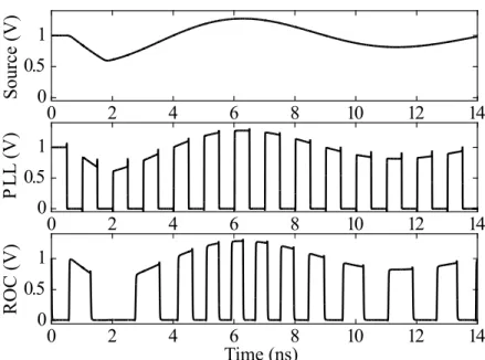
5.7 Critical path delay, and the clock period of the PLL and the ROC, for the activity patterns of Fig. 5.4(e) and Fig. 5.4(j). . 90
5.8 Largest delay increase vs. the distance between the ROC and the critical path (200nF decaps, activity at 1GHz). . . 91
5.9 Delay increase in the clock period for each activity pattern, for the PLL and the ROC (200nF of on-chip decaps, activity at first droop). . . 91
5.10 Impedance response of the PDN with 200nF, 300nF, 400nF and 500nF of on-chip decoupling capacitance. . . 93
5.11 Delay increase for the PLL and ROC, with different amounts of on-chip decoupling capacitance. . . 94
5.12 Normalized leakage power and minimum voltage for different amounts of on-chip decoupling capacitance (activity at 1GHZ). 95 5.13 Normalized leakage power and minimum voltage for different amounts of on-chip decoupling capacitance (activity at first droop frequency). . . 96
is a black circle, and VSS connection is a white circle). . . 96 5.15 Impedance response of all grid points (200nF of on-chip
ca-pacitance) with (a) 36 bumps distributed and (b) 40 bumps in the borders. . . 97 5.16 Voltage distribution for activity pattern of Fig. 5.4(j) with (a)
36 VDD/VSS bumps distributed (Vmin = 0.872V), and (b) 40 VDD/VSS bumps in the borders (Vmin = 0.837V). . . 97 5.17 Required margins for the PLL and ROC with different bump
placements (200nF of decoupling capacitance, activity at 1GHz). 98 5.18 Impedance responses with 500nF of on-chip capacitance and
different package decap parasitics. . . 99 5.19 Required margins for the PLL and ROC with the different
package decap parasitics (500nF of on-chip decaps, activity at first droop). . . 100 5.20 Power/Performance trade-off for ±10% voltage noise. . . 101 5.21 Frequency spectrum comparison of ROC vs. PLL. . . 102
List of Tables
2.1 Example of truth table for a Boolean functionF1 :B3 →B1. . 14
2.2 Boolean algebra properties. . . 19
2.3 K-cuts enumeration for the AIG in Fig. 2.5. . . 22
3.1 Results obtained through AIG transformations. . . 40
3.2 Divisors accepted based on the divided function f. . . 45
3.3 AIG results of Boolean decomposition. . . 46
3.4 Technology mapping results. . . 47
4.1 Comparison of the FPGA mapping for the AIGs obtained via algebraic factorization and support-reducing decomposition. . 54
4.2 FPGA mapping comparison with BDD-based approaches (k= 5). . . 66
4.3 FPGA mapping comparison for the 20 largest MCNC bench-marks (k= 6). . . 68
4.4 FPGA mapping of 20 largest MCNC benchmarks (k = 6) for MFS [82], BDS-pga [114], ABC and SR-map. . . 69
4.5 Best known results for EPFL benchmarks. . . 71
4.6 Remapping of the commercial tool results for the 20 largest MCNC benchmarks (k = 6). . . 72
4.7 Results of a commercial tool for different strategies, after phys-ical synthesis (post place-and-route). . . 73
4.8 Results of a commercial tool after physical synthesis using the initial description as input. . . 75
4.9 Results of a commercial tool after physical synthesis using the SR-map (area) + ABC (delay) remapping as input. . . 76
4.10 Results of a commercial tool after physical synthesis using the SR-map (delay) + ABC (delay) remapping as input. . . 77
5.1 PDN parameters . . . 84
Chapter 1
Introduction
On September of 2018, the integrated circuit (IC) celebrated 60 years of its invention [51]. This tiny electronic component, also known as chip, caused one of most important technological progresses in human history: the digital revolution. All areas of knowledge have taken advantage of the IC, gen-erating remarkable improvements at a much faster rate than ever before. Nowadays, there are far more chips than people on earth. They are present in computers, phones, televisors, medical devices, cars, trains, airplanes, and virtually everywhere with the introduction of theinternet of things (IoT) [9]. Notwithstanding, ICs are also the underlying reason for the existence of mul-tiple things: laptops, smart phones, self-driving cars, wearable devices, space exploration, the Internet, and consequently, all Internet-related services.
An IC is a miniaturized electronic circuit [51] manufactured with semi-conductors, and designed to perform one or more logic functions. The solid-state transistors [108] are the on-off switches which turned out to be the basis for the implementation of integrated circuits. In 1965, Gordon Moore noticed that the number of transistors per chip doubled every year [91] since the invention of the IC in 1958. After reaching the first limitations of the
complementary metal-oxide-semiconductor (CMOS) technology, Moore pre-dicted that this trend would continue, but at a more conservative rate: the number of transistors on a chip would double every 2 years [92]. This pre-diction, later on calledMoore’s law, helped to drive the progress of the semi-conductor industry ever since. This evolution was made possible by a large number of factors. For instance, the reduction of the transistor size shown in Fig. 1.1 (minimum feature size). In the course of 60 years, the minimum fea-ture size scaled ≈ 3500×, reaching 7nm in 2018. Furthermore, ICs enabled the development of workstations, also emerging the industry of electronic design automation (EDA), producing a self-reinforcing virtuous cycle which continually pushed forward the state-of-the-art [1].
Figure 1.1: Evolution over time of the transistors density and the minimum feature size (Source: [36]).
In the early days, ICs were designed by hand, using engineering paper and color pencils. The masks for lithography were made out of rubylith [74], and manufacturing was performed with primitive planar technology. Several
computer-aided design (CAD) tools were developed with the first computers: to help with the artwork and the routing of wires connecting transistors, and for circuit simulation (SPICE). During the 1980s, physical synthesis tools emerged, and circuits started to be described atregister-transfer level (RTL) with the aid of ahardware description language (HDL), changing completely the methodology which ICs were designed. Soon after, the system behavior could be described in HDL and transformed into a netlist of logic gates, arising the field of logic synthesis.
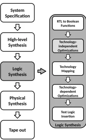
Thestandard cell methodology shown in Fig. 1.2 is one of the factors that pushed forward Moore’s law, reachingvery-large-scale integration (VLSI) cir-cuits. It is based on a limited set of digital logic gates (a cell library), with a standard height for all cells, and a rigid window of operation: theclock. This methodology is also known as application specific integrated circuit (ASIC) design flow, and can be divided intohigh-level synthesis (HLS), logic synthe-sis, and physical synthesis. HLS makes transformations at an architectural level, transforming a C-like algorithmic description into an RTL. Logic syn-thesis is responsible for the transformation of the circuit behavior description into a netlist of logic gates for a given technology, i.e., a digital mapped cir-cuit [34]. The physical synthesis transforms the netlist derived by logic syn-thesis into a set of geometric shapes, which represent the different layers to be manufactured. Floor plan, placement,clock tree synthesis (CTS), routing and design rule checking (DRC) are some steps of physical synthesis [5].
Technology- dependent Optimizations RTL to Boolean Functions Technology-independent Optimizations Technology Mapping Test Logic Insertion System Specification Tape out Physical Synthesis Logic Synthesis High-level Synthesis Logic Synthesis
Figure 1.2: Logic synthesis in the standard cell flow of integrated circuits.
Logic synthesis is a key process in order to produce a chip with high
quality of results (QoR). It can be divided into five steps. The first step consists of transforming the RTL description into a technology-independent representation, e.g., Boolean networks orand-inverter graphs (AIGs). Then, several optimizations are performed on this representation, reducing cost functions regarding area and delay. The following step is technology map-ping, matching parts of the circuit representation to logic gates of a library. Several optimizations can be performed on the mapped circuit, such as re-ducing delay in order to meet the constraints, and rere-ducing area and power consumption as low as possible. The final step is the test logic insertion.
Overall, logic synthesis methods try to minimize the number of com-ponents, delay and power consumption. Notice that functionally equivalent circuits with fewer components imply fewer transistors and lower costs. Mak-ing a circuit faster means to have the same outcome in less execution time, which is also desirable. The autonomy of portable devices based on batteries, the limitation for heat dissipation (and its impact on performance) of many devices are some of the reasons to have low power consumption as a goal.
1.1
Research motivation and goal
The scaling of the transistor size has historically resulted in reduction of costs, higher performance and lower power. Some reasons for this behavior are: the ICs are smaller and more chips can be manufactured in the same wafer, the capacitances are reduced, and lower voltages were required. However, the technology scaling is reaching a physical (and economical) limit [115].
The unavoidable heat generated by millions of devices jammed in the same small piece of semiconductor is a problem, generating issues such as
dark silicon [35]. It is also worth noting that silicon is the most used semi-conductor for manufacturing of ICs, and the feature size of 5nm predicted to 2020 also means that there will be features of ≈ 10 atoms in size [112]. At this point, quantum uncertainties will increase significantly the variability of devices, e.g., resistance, capacitance, and delay. The evolution of manu-facturing technologies also has inherently high costs, with more photolithog-raphy steps, different machines, and a large amount of design rules. The investment of building a new foundry to scale down the feature size is in the order of billions of dollars, which has a decreasing economical appeal [19].
Many different technologies have been investigated in order to substitute CMOS and continue the exponential improvements witnessed in previous decades. The ideas researched range from quantum [94] and neuromorphic computing [47], to graphene compounds [63] and spintronic materials [118]. Nevertheless, no CMOS substitute has made into production until now.
In the past, when CMOS limits were hit, it did not result in the end of the IC. Improvements will happen a slower rate, and come from different areas instead of transistor scaling. Even if no changes are perceived in transistor density, performance will be increased and costs will be reduced due to better manufacturing productivity, cycle time reduction, defect elimination, and the design of more powerful EDA tools. Note that the semiconductor industry currently has a worldwide revenue of ≈ 450 billion dollars per year, and it continues to reinvent itself, exploring artificial intelligence (AI) [59], cloud computing [7], and hardware acceleration [100].
Many experts believe that improvements will continue to happen in the foreseeable future [30]. The field-programmable gate array (FPGA) is one of the potential driving forces of the industry. FPGAs emerged in the late 1980s, composed of small memory blocks, which are used to implement combina-tional and sequential logic, in an array of programmable interconnections. An FPGA with ≈ 30 billion transistors, which implement 5.5 million logic elements, is commercially available since 2016 [48]. Clearly, EDA methods must be updated in order to deal with the size and complexity of such large ICs, while maintaining or improving the QoR of the final implementation.
Logic synthesis is one of the topics of this thesis. The algorithms involved in logic synthesis perform extremely complex tasks, with many variables to be considered, and trying all possibilities is not computationally affordable. The necessity of having reasonable solutions within time-to-market leads to multiple heuristics, generating sub-optimal results. Notice that the results obtained by state-of-the-art logic synthesis tools still have room for improve-ment, and finding optimal solutions may be feasible only for small circuits. Additionally, for numerous reasons, digital circuits typically operate with rigid clock sources. However, the size and complexity of current ICs lead to excessively conservative timing margins, and consequently, performance degradation and increased costs. Considering these possibilities, the main goal of this thesis is to explore alternatives in order to produce faster and cheaper ICs, even with the established CMOS technology.
1.2
Contributions of this thesis
In this thesis, alternatives to improve power, performance, area, and cost
(PPAC) in the established CMOS technology are proposed. This work ex-plores advances in EDA for three different topics: area minimization using Boolean methods, area and delay reduction for designs based onlook-up tables
(LUTs), and an alternative clocking scheme in order to improve performance, leakage power and costs. Specifically, the proposed contributions are:
1. A technology-independent method for area minimization of combina-tional logic, based on a multi-output decomposition using two-literal divisors (see Chapter 3).
2. A functional decomposition which uses the support size as cost func-tion, and a recursive remapping approach targeting LUT-based FPGAs (see Chapter 4).
3. An analysis on dynamic variability mitigation and simplification of
power delivery networks (PDNs) using an adaptive clocking scheme based on ring oscillator clocks (ROCs) (see Chapter 5).
The remaining of this section provides a summary of these contributions.
1.2.1
Boolean decomposition using two-literal divisors
Optimization techniques applied in technology-independent representations are typically limited to single-output transformations. Additionally, these techniques are highly biased by the structure, leading to sub-optimal results.
The work presented in Chapter 3 proposes a method for area minimization, exploring multi-output decomposition and Boolean methods, which offer less structural bias. Small parts of the circuit with multiple outputs are identified, and Boolean division using two-literal divisors is applied in order to increase logic sharing. This contribution presents the following characteristics:
• Boolean decomposition with two-literal divisors [90] is generalized from single-output to multi-output functions.
• The selection of divisors is customized to increase the logic shared among multiple outputs.
• A set of filters is proposed to reduce the search space.
• Area minimization is achieved by iteratively applying Boolean decom-position to KL-cuts [69, 75] of the circuit representation.
These contributions have been published in the following paper: [66] Lucas Machado, Jordi Cortadella. Boolean Decomposition for AIG Optimization. InProceedings of ACM Great Lakes Sym-posium on VLSI (GLSVLSI), pages 143-148, May 2017
1.2.2
Support-reducing logic decomposition and
remap-ping
The cost functions for most decomposition methods were defined due to the high correlation with the area of cell-based designs, e.g., literals, cubes. However, these cost functions have a weaker correlation for FPGAs based on LUTs. Moreover, local optimizations have limited power due to the structural bias of the circuit descriptions, which are typically designed for ASICs. The work presented in Chapter 4 proposes the reduction of the structural bias by remapping the LUT network and decomposing the derived functions using the support size as cost function. The two main contributions are:
1. A functional decomposition, which is guided by the support size, and it is based on simple and fast support-reducing techniques.
2. A recursive remapping approach, that reduces the structural bias of the subject graph, and uses the FPGA mapping metrics as cost function. The methods are able to improve several best known results of the EPFL benchmarks [6], and obtain significant improvements in comparison with the results of a commercial tool. The reasons for these improvements are the following.
• The mapping result is used to guide the resynthesis algorithm, instead of literals and cubes. This cost function reduces the miscorrelation between intermediate and final results, accepting transformations that will contribute to improve the final solution.
• A recursive collapsing strategy is applied instead of a local partial col-lapsing, which reduces the structural bias of the subject graph.
• Also, additional structures are explored, which are generated by a support-reducing functional decomposition. Notice that the support size as cost function makes sense for FPGAs: a k-input function with
any number of literals can be implemented with a single LUT of k inputs.
These contributions have been published in the following papers: [68] Lucas Machado, Jordi Cortadella. Support-Reducing Func-tional Decomposition for FPGA Technology Mapping. In Pro-ceedings of International Workshop on Logic & Synthesis(IWLS), pages 79-86, June 2018
[67] Lucas Machado, Jordi Cortadella. Support-Reducing Decom-position for FPGA Mapping. InIEEE Transactions on Computer-Aided Design of Integrated Circuits and Systems (TCAD), 2018 (Accepted for publication)
1.2.3
Voltage noise mitigation using ROCs
Variability, static or dynamic, is one of the biggest challenges in current ICs. Typically, variability is considered by adding guard band margins to the nominal clock period. However, this has led to excessively conservative timing margins, degrading performance. Voltage noise is the main source of dynamic variability and a major concern for the design of PDNs. Lower supply and threshold voltages were made possible with technology scaling, but power density was also increased. Consequently, power integrity became a key factor in the design of reliable high-performance circuits.
ROCs have been proposed as an alternative to mitigate the negative ef-fects of voltage noise. The capability of reacting instantaneously to large voltage variations makes ROCs an attractive solution, which also allows to relax the constraints required for the PDN design. However, the effectiveness highly depends on the design parameters of the PDN, power consumption patterns, and the spatial locality of the ROC within the clock domains.
The work in Chapter 5 presents an analysis on voltage locality for a de-sign using ROCs as clock source. Voltage locality is introduced by multiple activity patterns using an on-chip power distribution model. A trade-off between the number of ROC domains and performance is presented. Also, modifications in the PDN are evaluated, such as removing on-chip decoupling capacitance and changing the number and placement of the power bumps. The goal of this work is to present a conservative analysis of the benefits of using ROCs when dealing with problems related to voltage noise. Robustness to voltage noise is achieved without degrading performance, making possi-ble the simplification of the PDN design. These contributions have been published in the following papers:
[71] Lucas Machado, Antoni Roca, Jordi Cortadella. Increasing the Robustness of Digital Circuits with Ring Oscillator Clocks. In Proceedings of the International Workshop on Resiliency in Embedded Electronic Systems (REES), pages 29-34, March 2017
[72] Lucas Machado, Antoni Roca, Jordi Cortadella. Voltage Noise Analysis with Ring Oscillator Clocks. In Proceedings of IEEE Computer Society Annual Symposium on VLSI (ISVLSI), pages 1-6, July 2017
[73] Lucas Machado, Antoni Roca, Jordi Cortadella. Robustness to Voltage Noise with Ring Oscillator Clocks. In IEEE Transac-tions on Nanotechnology (TNANO), 2018 (Under review)
1.3
Manuscript organization
This thesis is structured into 6 chapters. The present chapter constitutes an introduction to the thesis. The remaining of this thesis is organized as follows.
Chapter 2: Background - This chapter provides a set of important prelim-inary information regarding all contributions of the thesis, organized in two main sections: logic synthesis and adaptive clocking.
Chapter 3: AIG Optimization via Boolean Decomposition - This chapter investigates area minimization using AIGs, exploring Boolean methods in or-der to reduce the number of nodes. Boolean division with two-literal divisors is applied to multi-output functions, and AIGs are minimized through local optimization.
Chapter 4: Support-reducing Decomposition for FPGA Mapping - This chapter proposes two methods targeting LUT-based FPGAs. A functional decomposition approach which uses the support size as cost function, ex-ploring the inherent characteristics of FPGAs. Also, an recursive remapping method is proposed, which reduces the structural bias of the subject graph and uses the mapping results as cost function, obtaining significant reduc-tions in area and delay.
Chapter 5: Robustness to Voltage Noise with Ring Oscillator Clocks- This chapter presents an analysis of dynamic variability mitigation using an adap-tive clocking scheme based on ROCs. The impact of the PDN parameters and ROC location on the robustness to voltage noise are investigated. Several PDN simplifications are analyzed, showing that tolerance to voltage noise and related benefits can be increased with multiple ROC domains.
Chapter 6: Conclusions and Future Work - The final chapter concludes the thesis, presenting a summary of the contributions and providing ideas for future research based on the present manuscript.
Chapter 2
Background
This chapter presents two main sections that provide important concepts regarding the contributions of the thesis. Section 2.1 presents background for the contributions in logic synthesis, whereas Section 2.2 introduces topics regarding adaptive clocking.
2.1
Logic synthesis
Logic synthesis is an important area of study in the field ofelectronic design automation (EDA), being responsible for the transformation of a circuit be-havioral description into a netlist of gates for a technology, i.e. a mapped circuit. Typical objectives of the logic synthesis are to reduce area, delay, power, or a combination of these. This section presents the background for the thesis contributions on logic synthesis, presented on Chapters 3 and 4.
2.1.1
Boolean functions
The Boolean domain is defined as B = {0,1}, where 0 and 1 represent two well-defined logic states, such as true (1) and false (0). An n-dimensional Boolean space Bn is composed of 2n distinct Boolean vectors of length n.
For instance, B1 ={0,1}, B2 ={00,01,10,11}, and so on.
A completely specified Boolean function can be described as a mapping between Boolean spaces [34]. A Boolean function with n inputs and m out-puts (n, m ∈ N) can be represented with the mapping: Bn → Bm. It is a
single-output function if m = 1, and it is a multi-output function ifm >1. An incompletely specified function (ISF) is defined over a sub-set of Bn,
where there are undefined function points, which are also known as don’t care (DC) conditions. In another definition, an ISF can be represented as
Bn → {0,1,−}m, where ‘−’ denotes a DC value, i.e., it can be either ‘1’
or ‘0’. The sub-domains of the function F that evaluate to 1, 0 and − are denoted the ON-set, the OFF-set, and the DC-set, and can be represented by the completely specified functions FON, FOFF and FDC, respectively. If
the DC-set is empty, then the function is completely specified.
2.1.1.1 Boolean operations
There are three basic Boolean operations: negation (or complement) (NOT), conjunction (AND), and disjunction (OR). The negation is a unary operation, i.e., it is in the Boolean space B1, whereas the conjunction and disjunction are operations between two or more Boolean variables. Consider the Boolean variablesx and y. The negation of x is denoted by x, and its result isx= 0 ifx= 1, and x= 1 ifx= 0. The AND operation can be denoted byx
·
y (or xy), and its result is x·
y= 1 ifx=y= 1, and x·
y = 0 otherwise. The OR operation can be represented asx+y, and its result isx+y= 0 ifx=y= 0, and x+y = 1 otherwise.Another important Boolean operation is the exclusive-or (XOR). The XOR operation is denoted by x⊕y, and its result is x⊕y= 0 if x=y, and x⊕y= 1 ifx6=y. The exclusive-or can also be described in the conjunctive and disjunctive forms: (x
·
y) + (x·
y) and (x+y)·
(x+y), respectively.2.1.1.2 Cofactors
Consider the Boolean functionF(X) :Bn→B1. Thesupport ofF is the set of variables X = (x1, x2, . . . , xi, . . . , xn), and the support size is denoted by |F|. A Boolean variable xi ∈X is considered to beessential for the function
F if there are at least two elements in Bn that are different only due to xi.
The positive cofactor of F with respect to variable xi ∈ X consists of
assigning xi to ‘1’, i.e., Fxi =F(x1, x2, . . . ,1, . . . , xn). Similarly, the negative
cofactor of F with respect to variable xi is obtained by assigning xi to ‘0’,
i.e., Fxi =F(x1, x2, . . . ,0, . . . , xn). If the negative and the positive cofactors with respect a variable xi are equal, i.e., Fxi = Fxi, then the variable xi is not in the support ofF. A cube-cofactor consists of performing the cofactor operation recursively, e.g., assigning the variables {xi, xj} ⊆ X in F(X) to
xi = 0 andxj = 1, which can be denoted asFxixj.
Cofactors can be used to extract information from F with respect to a variable in its support. One of the most important operations based on cofac-tors is the Boole’s expansion theorem, also known as theShannon expansion
or decomposition, which is described in (2.1).
There are also other important operations based on cofactors: theBoolean difference (or derivative) in (2.2), the existential abstraction (or smoothing) in (2.3), and the universal abstraction (or consensus) in (2.4).
δF/δxi =Fxi⊕Fxi (2.2)
∃xiF =Fxi+Fxi (2.3)
∀xiF =Fxi
·
Fxi (2.4)The Davio expansion is another decomposition based on cofactors, us-ing the XOR operation and the Boolean difference. There are two Davio expansions: the positive (2.5), and the negative (2.6) forms.
F = (xi
·
δF/δxi)⊕Fxi (2.5)F = (xi
·
δF/δxi)⊕Fxi (2.6)2.1.1.3 Unateness and containment
A Boolean function F is positive unate in the variable xi ifFxi ⊇Fxi, where ⊇ is the set operation of inclusion. Similarly, F is negative unate in the variable xi if Fxi ⊇ Fxi. Otherwise, xi is considered a binate variable in F. This is the concept of unateness [34], intended for completely specified functions. If a function F has only positive and negative unate variables, then F is considered unate. If F has one or more binate variables, then it is a binate function.
Containment[116] is a generalization of the concept of unateness for ISFs. There is a containment in the function G of the variable xi in the positive
polarity if
(GDCxi ∪GONxi)⊇GONxi, and a containment in the negative polarity if
(GDCxi ∪GONxi)⊇GONxi,
where the operator∪ is the set operation of union, GON is the ON-set of G,
and GDC is the DC-set of G.
2.1.2
Representation of Boolean functions
There are multiple forms to represent a Boolean function, each of them with a characteristic: canonicity, scalability, expressivity, etc. This section presents the representations used in the work proposed by this thesis: truth tables, Boolean expressions, binary decision diagrams (BDDs), Boolean networks, and and-inverter graphs (AIGs).
Table 2.1: Example of truth table for a Boolean functionF1 :B3 →B1. x1 x2 x3 F1 0 0 0 0 0 0 1 0 0 1 0 0 0 1 1 1 1 0 0 0 1 0 1 1 1 1 0 0 1 1 1 1 2.1.2.1 Truth tables
Truth tables are a straightforward representation of Boolean functions. A truth table can be partitioned into two parts: on one side, all possible com-binations of the input variables are described; on the other side, the values of output variables are set according to the respective input combination. Ta-ble 2.1 shows an example of truth taTa-ble for a Boolean functionF1 :B3 →B1. The input vectors that evaluate the function to ‘1’ are the ON-set, e.g.,
{011,101,111}. Similarly, the input vectors that evaluate F1 to ‘0’ are the OFF-set, e.g., {000,001,010,100,110}. Truth tables are a canonical repre-sentation, given the same variable order.
2.1.2.2 Boolean expressions
A single-output Boolean function can also be represented as a Boolean ex-pression. In this case, the Boolean operators are applied to the input variables of the function in order to represent its functionality. Each time a Boolean variable appears in a Boolean expression, negated or not, it is considered as one literal. Boolean expressions with fewer literals are preferred, since these will likely require less logic elements to be implemented. Notice that a Boolean expression represents exactly one Boolean function, but a Boolean function can be represented by multiple different Boolean expressions. For example, consider the function F1 from Table 2.1.
Canonical sum-of-products: Extracting the Boolean vectors that eval-uate F1 to ‘1’, and representing them as Boolean expressions, in order to implement the correct functionality ofF1, the result obtained is described in (2.7), which is asum-of-products (SOP).
Canonical product-of-sums: Similarly, considering the Boolean vec-tors that evaluate F1 to ‘0’ as Boolean expressions, the result obtained is a
product-of-sums (POS), which is described in (2.8).
F1 = (x1+x2+x3)(x1+x2+x3)(x1+x2+x3)(x1+x2+x3)(x1+x2+x3) (2.8)
Such SOP and POS are canonical, as they are translations of the Boolean vectors to expressions, applying logic operations to implement the Boolean function. However, these representations typically have several literals and cubes, with 9 literals (and 3 cubes) in (2.7), and 15 literals (and 5 cubes) in (2.8). SOP and POS are also two-level Boolean expressions, and two-level minimization [15] methods can be applied to reduce the number of literals.
Factored form: Further optimizations can be applied in order to reduce the number of literals, such as factorization [13, 76], generating Boolean expressions with unbounded number of levels. For instance, a factored-form expression of the function F1 is shown in (2.9), with 3 literals.
(x1+x2)x3 (2.9)
2.1.2.3 Binary decision diagrams
A BDD is another representation of Boolean functions [3]. BDDs are rooted,
directed acyclic graphs (DAGs) with two terminal nodes (0 and 1), and each nonterminal node represents a Boolean variable with two outgoing edges: the 0-edge and the 1-edge. The BDD representation of the functionF1 from Table 2.1 is shown in Fig. 2.1(a), where the dashed lines are the 0-edges, the non-dashed ones are the 1-edges, the circles represent the nonterminal nodes, and the squares are the terminal nodes. Notice that BDDs are based on the Shannon expansion. A reduced-ordered BDD (ROBDD) is a BDD in which the nonterminal nodes are organized in a fixed variable order, and the number of BDD nodes is reduced using minimization rules [17]. ROBDDs are a canonical representation, given the same variable order. In this work, ROBDDs are referred as BDDs. BDDs are an efficient representation (with a few exceptions) and are more scalable than other functional representa-tions, such as truth tables. Also, there are modern software libraries which efficiently implement BDD operations [109].
2.1.2.4 Boolean networks
Graphs are data structures widely used in computer science, due to their high expressivity and the many efficient algorithms for graphs. A graph
x
10
x
2x
31
x
3x
30
0
0
0
1
1
x
2x
2 (a) BDD x1 x2 x3 1 0 (b) ROBDDFigure 2.1: (a) BDD and (b) ROBDD of the functionF1 from Table 2.1.
and the set of edges E (or arcs), which connect two vertices. However, in order to represent Boolean functions, two constraints are required: (1) the edges must be directed; and (2) cycles are not allowed. These conditions coincide with DAGs, which are used to represent circuits.
ABoolean network (or logic network) is a DAG with three types of nodes: the primary inputs (with no incoming edges), the primary outputs (with no outgoing edges), and the internal nodes (or logic gates). The edges are di-rected from inputs to outputs. The internal nodes can represent anyn-input and m-output Boolean function. However, due to the limitation of appli-cation specific integrated circuit (ASIC) and field-programmable gate array
(FPGA) technologies, the logic nodes are typically reduced to functions with n≤6 andm≤2. This process of breaking a large function into smaller ones is performed by decomposition, which is explained in Section 2.1.3.
2.1.2.5 And-inverter graphs
An AIG [79] is a specific type of Boolean network in which each node has either 0 incoming edges - the primary inputs (PIs), 2 incoming edges - the
AND nodes, or 1 incoming edge - theprimary outputs(POs). The PI and PO nodes do not have a function associated, whereas the AND nodes perform the Boolean operation AND for two input variables. The edges can implement an NOT operation or not. Sequential elements are considered as PI/PO pairs. An example of AIG is shown in Fig. 2.2: the dashed lines indicate negated edges, the circles are AND nodes, the squares at the bottom are PIs, and the squares at the top are POs.
Using only the NOT and AND operations, AIGs are a simple and powerful data structure, and the state-of-the-art to represent very large circuits, e.g., thousands of inputs, millions of AIG nodes. However, AIGs are not canonical, i.e., the same Boolean function can be represented by different AIGs.
pi1
pi0 pi2 pi3 pi4
po2
po0 po1
Figure 2.2: Example of an AIG, with 15 nodes and 5 levels.
In technology-independent logic synthesis, it is not known the effective costs in the target technology. Therefore, different cost functions are used to predict the cost of the final circuit, such as literals in Boolean expressions. For AIGs, the area is correlated with the number of AND nodes, whereas the delay is proportional to the logic depth between the PIs and POs.
2.1.3
Logic decomposition
Logic (or functional) decomposition is a method of breaking a large, complex Boolean function into a set of smaller, simpler functions. Functional decom-position was introduced by Ashenhurst [8], expressing a Boolean function F(X) in terms of other Boolean functions Gand H:
F(X) =H(G(X1), X2), (2.10)
whereX1 6=∅, X2 6=∅, andX =X1∪X2. The setsX1 andX2 are known as bound-set and free-set, respectively. Only single-output functions are con-sidered in the Ashenhurst decomposition [8], and functional decomposition is extended to multiple-output functions in the work proposed by Curtis [31]. An example of decomposition is shown in (2.11).
F = (x1
·
x4) + (x2·
x3·
x4) +x5 decomposition −−−−−−−→ G=x1 + (x2·
x3) F = (G·
x4) +x5 (2.11)X2 X1 X3=∅ G1 G2 H F
(a) Disjoint support X2 X1 X3 G1 G2 H F (b) Strong X2=∅ X1 X3 G1 G2 H F (c) Weak
Figure 2.3: Examples of (a) disjoint, (b) strong, and (c) weak bi-decompositions.
2.1.3.1 Bi-decomposition
A bi-decomposition is a special case of functional decomposition in which the derived functions have two or fewer inputs, i.e., |H| ≤ 2. Given a function H, such that|H|= 2, F is bi-decomposable if it can be represented as:
F(X) = H(G1(X1∪X3), G2(X2 ∪X3)), (2.12) where X1 ∩X2 = ∅, X1 ∩X3 = ∅, X2 ∩X3 = ∅, andX =X1∪X2∪X3. If X3 =∅, then it is a disjoint-support decomposition (DSD), and such decom-positions [11, 77, 78, 18] are of special interest for their low implementation cost. If X1 6= ∅, X2 6= ∅, and X3 6=∅, then it is a strong bi-decomposition. Otherwise, if X1 = ∅ or X2 = ∅, then it is a weak bi-decomposition [87]. Fig. 2.3 shows schematics with examples of these decompositions. A bi-decomposition is also support-reducing if X1∪X3 < X and X2∪X3 < X.
Bi-decomposition algorithms typically perform decompositions based on the Boolean operations AND, OR and XOR, recursively reducing the size of the sub-functions. Such algorithms are top-down approaches, relying on cost functions to estimate the actual implementation cost. This characteristic may also impact the area results for the cases with potential logic sharing or hierarchy, and a following process for area recovery may be required.
2.1.3.2 Algebraic and Boolean division
Logic synthesis algorithms can be divided into two groups: (1) the alge-braic methods, which consider the Boolean functions as polynomial expres-sions, and (2) the Boolean approaches. Table 2.2 presents all the properties considered in Boolean approaches, whereas algebraic methods only consider properties {1,2,3,4,5,6,8,10} during transformations. On one hand, algebraic methods are very fast, but the quality of results are typically far from opti-mal. On the other hand, Boolean approaches are able to obtain better results, but also require much more execution time and memory consumption.
Table 2.2: Boolean algebra properties. # Property Expression 1 Associativity x+ (y
·
z) = (x+y)·
z 2 x·
(y+z) = (x·
y) +z 3 Commutativity x+y=y+x 4 x·
y=y·
x 5 Identity x+ 0 =x 6 x·
1 =x 7 Annihilator x+ 1 = 1 8 x·
0 = 0 9 Distributivity x+ (y·
z) = (x+y)·
(x+z) 10 x·
(y+z) = (x·
y) + (x·
z) 11 Idempotence x+x=x 12 x·
x=x 13 Absorption x·
(x+y) =x 14 x+ (x·
y) =x 15 Complementation x·
x= 0 16 x+x= 1 17 De Morgan x·
y =x+y 18 x+y=x·
y 19 Double negation (x) =xThe concept ofdivisionof a Boolean functionF is given by the expression F = (D
·
Q) +R, where the Boolean functions D, Q and R are the divisor, quotient and remainder, respectively. The function D is called a divisor of F if R 6= 0, and a factor if R = 0. The division operation can be performed by algebraic or Boolean means.A common approach to perform Boolean division is by using two-level minimizers that accept don’t care information [34]. A new variable x is added and the division is performed by adding the satisfiability don’t care
(SDC) expression x⊕d to the DC-set of F, where ⊕ represent the Boolean exclusive-OR operator, followed by a two-level minimization.
Example: Consider the function F = (abc) + (a+b)d represented as a fac-tored form with 6 literals. It is possible to rewrite F asF = (abc) + (xd) by performing algebraic division, using the divisor x= a+b. Boolean division can be performed by incorporating x⊕(a+b) in the DC-set and running a two-level minimization [15]. This process results in F = (acx) + (xd), which can be represented as the factored form with 4 literals: F = ((ac) +d)x.
Figure 2.4: Example of a 1×1 window on top of a DAG (Source: [83]).
2.1.4
Local optimization
Boolean methods are more powerful, but also computationally more expen-sive in comparison with algebraic methods. In order to take advantage of Boolean methods, a known approach is to apply the transformations only to a part of a Boolean network at a time. Limiting the scope of the logic synthesis, also known as local optimization, is crucial for the scalability of many logic synthesis algorithms, specially considering the increasingly large Boolean networks used in the semiconductor industry.
2.1.4.1 Windowing
Another method to perform local optimization is windowing, which was in-troduced in [88]. The approach consists of gathering nodes around a node N, given some parameters. An example of a window is shown in Fig. 2.4.
The leaf and the root set are non-overlapping sets of DAG nodes, such that every path from the primary inputs to any node in the root set passes through some node in the leaf set. The window is composed of every node in the paths between the leaf set and the root set, including the root set, and excluding the leaf set. The leaf and root nodes are shaded in the window of Fig. 2.4, denotedL and R, respectively.
A window is typically denotedn×m, wherendenotes the number of levels towards the primary inputs, andm define the levels in the outputs direction. For example, the window presented in Fig. 2.4 is 1×1, where the nodes I1 and O1 are obtained from the fanin and the fanout of N, respectively.
A reconvergence computation is also typically performed, in order to iden-tify a more significant portion of a DAG. TheS nodes comprise the intersec-tion of the fanins of O1 nodes and the fanouts of I1 nodes, given a distance
in levels of n+m. The leaf nodes (L) do not belong to S, but feed at least one of the nodes in S. The root nodes (R) belong to the set of S nodes, and also feed at least one node not in S. The nodes marked asP are obtained in the reconvergence process, as they are not connected directly to N, and are not leaf nor root nodes.
2.1.4.2 K-cuts
A K-feasible cut (or K-cut) of a noden is a subgraph (or a logic cone) rooted in the nodenand with no more thanK inputs. It is a useful method in AIG transformation algorithms [84], and in FPGA technology mapping [86].
Formally, a cut of a node n in a graph G is a set of nodes c such that every path between a primary input and n contains a node in c. A cut is irredundant if no subset of it is also a cut. If a cut is composed of one node, then it is a trivial cut. A K-cut [85, 95] of a node n in the graph G is an irredundant cut c with K or fewer nodes. The region defined by a K-cut is composed of all nodes in the path betweencandn, including the nodenand excluding the nodes in c.
The enumeration of K-cuts is realized by combining the cuts of the inputs of a node, where each cut is a set of nodes, and a union of these two sets is performed. Notice that the union of two K-cuts does not guarantee that the cut generated is K-feasible, therefore the enumeration process must remove any cut with more than K nodes. Consider the two sets of cuts A and B and the auxiliary set operation ./ described in (2.13). The ./ set operation removes the redundant cuts, and it is commutative, as the union set operation
∪ is also commutative.
A ./ B ≡ {a∪b |a∈A, b∈B,|a∪b |< K} (2.13) Given that ΦK(n) is the set of K-cuts ofn ∈ G and, ifn is not a primary
input or output, that n1 and n2 are its inputs. Then, ΦK(n) is defined
recursively [20], as described in (2.14). ΦK(n) = {{n}}, n is a PI {{n}} ∪ {ΦK(n1)./ΦK(n2)}, otherwise (2.14) K-cuts are considered a method to derive sub-circuits compared to win-dowing, as the support size is controlled, and the reconvergence paths are identified. However, notice that the number of K-cuts grows exponentially with K, and for this reason different classes of K-cuts have been explored, such as factor cuts [20] and priority cuts [86]. An example of graph covering using K-cuts is shown in Fig 2.5. Given that K = 4, the K-cuts enumerated for each node is described in Table 2.3.
Figure 2.5: Example of a graph covering with K-cuts (Source: [20]). Table 2.3: K-cuts enumeration for the AIG in Fig. 2.5.
Node K-cuts p {p} q {q} a {a},{p, q} b {b} y {y},{a, b},{p, q, b} c {c} d {d} z {z},{c, d} x {x},{y, z},{y, c, d},{a, b, z}, {a, b, c, d},{b, p, q, z} 2.1.4.3 KL-cuts
K-cuts are an efficient way to represent a region of a graph regarding a single output. However, several K-cuts may be necessary to cover regions with multiple outputs, duplicating logic. A KL-cut [75, 69] identifies a multiple-output region in order to overcome this issue. A KL-cut is a sub-graphGKL
of a graph G with K inputs and L outputs. It is represented as two sets of nodes: the inputs GK, and the outputsGL.
If a node n belongs to a path between nK ∈ GK and nL ∈ GL, being
n /∈ GK, thennis contained inGKL. Notice that all nodes inGLare contained
in GKL, and GKL does not contain any node of GK. The same algorithms
used to enumerate K-cuts can be used to identify L-cuts, controlling both the number of inputs and outputs of a region. However, in the work of Chapter 3, the number of outputs is not restricted in KL-cuts enumeration, as in [70]. Therefore, for every K-cut of a noden, there is aunique KL-cut GKL.
50 30 51 31 52 40 53 41 32 33 14 20 12 21 22 23 11 10 1 13 2 3 4 5 6 8 7 31
Figure 2.6: Example of KL-cut computation.
The nodes that are part of GKL are identified by traversing forward the
graph G from GK. A node n is part ofGKL if at least one of the K-cuts ofn
is a subset of or equal to GK. A node of GKL is contained in GL if it has a fanout to a primary output, or to a node not contained in GKL.
Example: Figure 2.6 depictsGK ={3,4,5,6,10,13} with its nodes in light
gray, which is one of the K-cuts of the node 31, in dark gray. The KL-cutGKL
is obtained by traversing the AIG forward fromGK, identifying the sub-graph
hatched in Fig. 2.6. Nodes 31 and 40 have fanout to POs, and nodes 12 and 33 have fanout to nodes not contained in GKL, therefore GL = {12,31,33,40}
is defined. Note that the logic of GL nodes can be described as Boolean
functions that depend on the same support, i.e., the GK nodes.
2.1.5
Collapsing
Collapsing [27] a Boolean network means to replace it by another network with one node for each output, with each node representing the Boolean func-tion of a primary output based solely on the primary inputs. This approach can be helpful as it removes structural redundancies from the logic network. The process of collapsing a circuit may be performed partially or globally.
Partial collapsing (or elimination) [23, 114] is an iterative process of re-moving nodes of a Boolean network by merging the function of a node with the ones in its fanout. The result is a Boolean network with a smaller set of
pi1
pi0 pi2 pi3 pi4
po2 po0 po1 011 1 100 1 010 1 111 1 collapse pi1
pi0 pi2 pi3 pi4
po2
po0 po1
Figure 2.7: Example of the collapsing process for a primary output.
nodes, but with more complex Boolean functions. The number of iterations, or the number of nodes merged, is typically limited by a cost function, e.g., literals, AIG nodes, BDD nodes. Notice that the effectiveness of this process is biased by the structure of the subject graph, and also by the order in which is performed, generating sub-optimal results.
For the work proposed in Chapter 4, collapsing is performed globally and for each output individually. The result of such collapsing process is the logic function of a primary output based on the primary inputs, as shown in the example of Fig. 2.7. The output function obtained is the same regardless of the circuit structure, therefore the structural don’t cares are removed [32]. Notice that logic sharing between outputs is potentially lost in this process, as observed in Fig. 2.7. This approach may result in larger area, but the possibilities of reducing circuit delay are increased. There are different ap-proaches for global collapsing, e.g., using a multi-rooted BDD, which perform partial logic sharing.
2.1.6
AIG transformations
AIGs offer an homogeneous data structure, in which simple, fast, and scal-able logic synthesis methods can be applied. The scalability is made possible by performing transformations on the AIG structure, using the number of nodes and the logic depth as cost function for area and delay, respectively. These AIG transformations are typically realized with fast local optimiza-tions, which can be repeated multiple times. After several iteraoptimiza-tions, the optimized AIG is the subject graph for technology mapping. This section reviews the main transformations used for AIG optimization.
Figure 2.8: Examples of AIG rewriting (Source: [84]).
The first step is to derive the AIG structure from an input description. In ABC [14], this is performed by running the command strash, which can be divided in two parts. The first part is to replace each node of the input Boolean network by the equivalent AIG structure, which is derived by the factorization [13] of the Boolean function of the node. The second part is the redundancy removal, which detects and merges isomorphic circuit structures. This process is also known asstructural hashing[79], which is performed using a hash-table, and ensures that there is only one node having the same pair of AIG nodes as fanins, considering permutation. After this process, it is said that the AIG is structurally hashed.
Refactoring [79, 84] is one of the methods for node count minimization. The method is implemented on the command refactor in ABC [14], and consists of iteratively extracting themaximum fanout-free cone (MFFC) for each AIG node, with a maximum of 16 variables. The logic function of the MFFC is factored [13], and the result of factorization is translated back to AIG format, replacing the original logic cone if the number of nodes is reduced (or not increased), and the logic depth is not increased.
Rewriting [79, 84] is another algorithm for minimizing the AIG size, enu-merating all K-cuts at each AIG node, and replacing them by functionally equivalent and smaller pre-computed cuts. Two examples of AIG rewriting are depicted in Fig. 2.8. The example at the top regards a simple substitution for a smaller structure, whereas the example at the bottom shows a replace-ment for a larger AIG, but taking advantage of nodes already present in the network. The command rewrite in ABC [14] implements this approach for cuts with up to 4 variables, using pre-computed AIGs indexed in a hash table with all 222 NPN-equivalent classes of 4-input functions [84]. This method can also be restricted to transformations that do not increase logic depth.
Figure 2.9: Example of a tree-balancing transformation (Source: [81]).
Balancing [27, 81] is a depth-aware transformation using algebraic tree-height reduction, performed by applying Boolean properties such as asso-ciativity, commutativity, and distributivity (see Table 2.2). An example of tree-balancing transformation is illustrated in Fig. 2.9. This algorithm [27] is also implemented in ABC [14] on the command balance, and it is frequently applied in between AIG node reduction approaches to minimize logic depth. Another method for AIG optimization is resubstitution [79], which tries to re-express the Boolean function of a node by reusing other nodes present in the AIG, also known as divisors. The method is implemented on the commandresubin ABC [14], and consists of iteratively extracting the MFFC for each AIG node, and rewriting the logic cone using k new nodes and removing l nodes. Similarly to other methods, if the number of nodes is reduced, i.e., l > k, then the modification is accepted. This approach can be considered a technology-independent version of the resynthesis methods based on resubstitution [53, 89].
It is also worth mentioning that AIG transformation methods are highly dependent on the input description. Therefore, a higher quality of results can be achieved by applying balancing, rewriting, resubstitution, and refactoring iteratively. For example, thedc2 command [82, 75] in ABC [14] iterates these methods in order to obtain an optimized AIG. Transformations that increase the number of levels are accepted if dc2 is executed without the -l option, therefore obtaining the minimum number of AIG nodes for this command.
2.1.7
FPGA technology mapping
Technology mapping is an important process in logic synthesis, which trans-forms a technology-independent circuit description into a network of gates from a given technology, i.e., a mapped circuit. This process can be divided into three steps: decomposition, matching, and covering.
![Figure 1.1: Evolution over time of the transistors density and the minimum feature size (Source: [36]).](https://thumb-us.123doks.com/thumbv2/123dok_us/10211167.2924468/22.892.219.738.200.441/figure-evolution-time-transistors-density-minimum-feature-source.webp)

![Figure 4.1: Correlation between the number of AIG nodes and LUTs after technology mapping (Source: [65]).](https://thumb-us.123doks.com/thumbv2/123dok_us/10211167.2924468/70.892.240.704.194.429/figure-correlation-number-nodes-luts-technology-mapping-source.webp)