FPGA-based High-Performance Parallel Architecture for
Homomorphic Computing on Encrypted Data
Sujoy Sinha Roy1,2, Furkan Turan1, Kimmo J¨arvinen3, Frederik Vercauteren1, and Ingrid Verbauwhede1 1KU Leuven, imec-COSIC, Belgium
2University of Birmingham, School of Computer Science, United Kingdom 3University of Helsinki, Department of Computer Science, Finland
1[email protected] 2[email protected] 3[email protected]
ABSTRACT
Homomorphic encryption is a tool that enables compu-tation on encrypted data and thus has applications in privacy-preserving cloud computing. Though conceptu-ally amazing, implementation of homomorphic encryp-tion is very challenging and typically software imple-mentations on general purpose computers are extremely slow. In this paper we present our domain specific ar-chitecture in a heterogeneous Arm+FPGA platform to accelerate homomorphic computing on encrypted data. We design a custom co-processor for the computationally expensive operations of the well-known Fan-Vercauteren (FV) homomorphic encryption scheme on the FPGA, and make the Arm processor a server for executing dif-ferent homomorphic applications in the cloud, using this FPGA-based co-processor. We use the most re-cent arithmetic and algorithmic optimization techniques and perform design-space exploration on different lev-els of the implementation hierarchy. In particular we apply circuit-level and block-level pipeline strategies to boost the clock frequency and increase the throughput respectively. To reduce computation latency, we use parallel processing at all levels. Starting from the highly optimized building blocks, we gradually build our multi-core multi-processor architecture for computing. We implemented and tested our optimized domain specific programmable architecture on Xilinx Zynq UltraScale+ MPSoC ZCU102 Evaluation Kit. At 200 MHz FPGA-clock, our implementation achieves over 13x speedup with respect to a highly optimized software implementa-tion of the FV homomorphic encrypimplementa-tion scheme on an Intel i5 processor running at 1.8 GHz.
1.
INTRODUCTION
Cloud services play an important role in our everyday life. When we update our Facebook status, check bank balance or upload photos on Instagram, we use cloud computers. In business applications, cloud services can be used for storing and processing information, ana-lyzing big-data, providing an environment for test and development, supporting cost-effective disaster recovery,
backing up files and so on [1]. However, cloud computing raises privacy issues. To compute on the data using cloud services, we need to deliver our data unencrypted. Since a cloud computer is a third-party resource, the owner of the cloud can see, use or abuse the unencrypted data. For instance, our internet search engine shows advertisements for cheap hotels or car rental just after searching for a flight. A cloud service provider may analyze business data of its clients for its own gain! Ho-momorphic Encryption (HE) is a tool to prevent invasion of users’ privacy while keeping the conveniences offered by the cloud services. HE enables computation on en-crypted data: users can upload their enen-crypted data to the cloud, and yet perform computations while it is kept encrypted (hidden from cloud owner). Some of the many interesting HE applications are: privacy-preserving ser-vices for information storage and processing in business and health-care applications [2], encrypted web-search engine [3], electronic voting, and privacy-preserving prediction from consumption data in smart electricity meters [4], machine learning on encrypted data [5] etc.
State of the art: Though, HE was conceptualized by Rivest, Adleman and Dertouzos [6] almost 40 years ago in 1977, the construction of a HE scheme that can compute ‘complex’ operations on encrypted data was an open problem until 2009 when Gentry came up with the first construction of such a scheme [7]. The first genera-tion of HE schemes including Gentry’s were extremely slow, hence did not provide a practical solution. Current generation HE schemes [8, 9] increased the performance by orders of magnitude; however, their software imple-mentations are still very slow. Recent implementation in a high-end GPU [10] reduce the computation time by several factors. Hardware accelerators offer parallel processing capabilities to achieve fast computation time. In the literature there are several reported hardware implementation that try to speedup performance of HE schemes [11, 12, 13, 14, 15, 16, 17, 18, 19, 20, 21]. Several of these reported implementations report only simulation based results. An actual hardware
implemen-tation requires additional building blocks to perform memory management, synchronization of parallel cores, and reliable interfacing with a host processor, etc. This makes implementation of complex HE schemes in hard-ware very challenging.
Our contributions:
During the Turing 2018 Award Ceremony, Hennessy and Patterson pointed out that domain-specific archi-tectures are going to be the computer archiarchi-tectures of the future as the performances of general-purpose com-puters are touching their limits. As HE is so complex, such general-purpose devices fail to satisfy a practical application. Therefore, we propose a domain-specific ar-chitecture for HE, implemented on an Arm+FPGA het-erogeneous platform, that could accelerate homomorphic computations on encrypted data in cloud installations. The hardware is used to accelerate the Fan-Vercauteren (FV) scheme which is a popular HE scheme and has been
implemented in several software libraries, e.g. FV-NFLlib
from CryptoExperts [22] andSEALfrom Microsoft [23]. Its hardware implementation poses unique challenges as it depends on dozens of modules in the design-hierarchy and their careful integration. We achieved high perfor-mance with parallel processing minimizing the number of cycles, and boosted the clock frequency with a pipeline datapath. In addition, multiple processors are instanti-ated at the higher level to distribute the computation.
We study the mathematical steps used in the sub-routines, analyze data dependencies and apply circuit-level pipeline strategy when constructing the building blocks for the complex sub-routines. At the higher level where the building blocks are connected, we ap-ply a block-level pipeline strategy and optimized task-scheduling to increase the throughput. To reduce the number of cycles, we instantiate multiple processing el-ements inside the building blocks after taking care of the data dependencies. Starting from these fast building blocks, we gradually construct our multi-core proces-sor architecture and implement it in FPGA to compute homomorphic operations on encrypted data.
We designed the hardware and its software counterpart in a Xilinx Zynq UltraScale+ MPSoC ZCU102 Evalu-ation Kit [24] and verified its correctness. With these optimization, our domain specific hardware architecture achieves 400 homomorphic multiplications per second at 200 MHz FPGA-clock, including hardware-software communication overhead. This is over 13x faster than a
FV-NFLlibbased highly optimized software running on an Intel i5 processor at 1.8 GHz clock frequency.
Last but not least, we share our work open source: https://github.com/KULeuven-COSIC/HEAT
The organization of this paper is as follows: A mathemat-ical background on homomorphic encryption is provided in Sec. 2. The parameters of the systemare presented in Sec. 3. Sec. 4 discusses the design decisions, approaches and algorithms used. Architecture details are provided in Sec. 5 and the implementation results shown in Sec. 6. The final section draws the conclusions.
2.
BACKGROUND
2.1
Homomorphic encryption
A homomorphic encryption scheme is an augmented encryption scheme with two additional routinesHE.Add()
andHE.Mult()to perform add or multiply on encrypted data. Due to its mathematicalhomomorphism, the result is still an encrypted data (calledciphertext) encrypting the sum or respectively the product of the plaintexts. Users can upload their ciphertext in an untrusted cloud and still perform computations on their ciphertext with-out the need for decryption.
Existing HE schemes are ‘noisy’ in nature. Noise is used to hide the message during encryption. With every homomorphic evaluation on the ciphertext, the noise in the result-ciphertext increases. There is also a noise threshold beyond which further homomorphic evalua-tions would result in decryption failures. This threshold value is called the ‘depth’ of the homomorphic scheme and it is determined by the choice of parameter set (e.g, length of data structures and size of coefficients etc.). In a simplistic view, ‘depth’ of a homomorphic encryption scheme is analogous to ‘critical path’ of a circuit. An HE scheme that supports a limited number of evaluations on ciphertext is called ‘Somewhat Homomorphic Encryp-tion (SHE).’ When an HE supports unlimited number of evaluations on ciphertext, it is called ‘Fully Homomor-phic Encryption (FHE)’ scheme. Existing constructions of FHE schemes start from a SHE scheme and use a complicated mechanism known as ‘bootstrapping’ on top to reduce the noise in the result. Though conceptually amazing, this bootstrapping mechanism requires a very large parameter set which adds a drastic performance penalty. In most real-life applications, the complexity (i.e., the depth) is bounded and hence application of SHE instead of FHE makes more sense. In the following sub-section, we briefly describe the well-known FV [9] SHE scheme for which we have constructed our domain-specific high-performance computer architecture.
2.2
FV SHE scheme
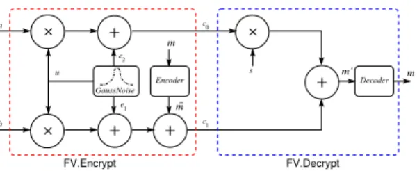
The FV SHE scheme was introduced by Fan and Vercauteren [9] in 2012. Like all other SHE schemes, FV performs ‘complicated’ mathematical operations. In this paper, we only provide a high-level description of the scheme, while details can be found in the original FV paper [9]. The FV scheme augments a Ring Learning With Errors (ring-LWE) public-key encryption scheme with two additional functionsAddandMultto perform addition and multiplication respectively on ciphertext. The encryption and decryption operations are described using a block diagram in Fig. 1.
All computations are performed in a polynomial ring R = Z[x]/hf(x)i with reduction polynomial f(x) =
Φd(x), the d-th cyclotomic polynomial of degree n =
ϕ(d). The ring is denoted asRq when the coefficients of
the polynomials reduced to moduloqwhich is an integer. All variables shown in Fig. 1 are degreen−1 polynomi-als. The public key is the pair (a, b) and the private is s. During encryption, the messagem is encoded, three
c0 c1 u e1 e 2 Encoder a m m~ m m’ FV.Decrypt b FV.Encrypt s GaussNoise Decoder
Figure 1: FV encryption and decryption.
polynomials (u, e1, e2) are sampled from an error distri-bution (typically a discrete Gaussian distridistri-bution) and then polynomial additions and multiplications are per-formed to generate the ciphertextcwhich consists of two polynomials (c0, c1)∈(Rq, Rq) with coefficients modulo
q. In practice, the coefficients of uare uniformly ran-dom signed binary numbers. The decryption performs a polynomial multiplication followed by an addition and finally decoding. The security of the encryption scheme relies on the ring-LWE problem which states that, given many tuples (ai, bi)∈(Rq, Rq), wherebi=ai·s+ei,ai
is uniformly random, andsandei are unknown
poly-nomials sampled from a proper error distribution, it is computationally unfeasible to compute the secrets.
Now we describe the Add and Mult functions that enable computation on ciphertext. Note that these are the two functions that are executed in the cloud and our hardware accelerator targets them. Let us consider two ciphertextsc0= (c0,0, c0,1) andc1= (c1,0, c1,1). FV.Add
simply adds the polynomials of the two input ciphertexts and outputs the result ciphertextc= (c0,0+c1,0, c0,1+ c1,1). FV.Mult is the most complicated operation and
it determines the noise growth in the ciphertext. The steps are shown using a block diagram in Fig. 2.
q Q Lift q Q Lift q Q Lift q Q Lift WordDecomp c ~ 0 c ~ 1 c ~ 2 c0,0 c0,1 c1,0 c1,1 c0 c1 Q q Scale Q q Scale Q q Scale 2 ReLin ReLin c ~ rlk rlk 0 1
Figure 2: FV homomorphic multiplication.
TheFV.Multuses additional routines, namelyLiftq→Q,
ScaleQ→q, WordDecompandRelin, besides polynomial
addition and multiplication. Liftq→Q is used to lift the
polynomials toRQ fromRq whereQis a much larger
modulus thanqand is in the order ofO(n·q2). Scale
Q→q
works in the reverse way, i.e., it scales polynomials from RQ toRq. WordDecompis used to decompose a
polyno-mial, saya∈Rq, in basewby slicing each coefficient ofa.
It returns a vector of polynomials (as shown using ‘bold’ font in Fig. 2). A toy example ofWordDecompfollows. If the polynomiala(x) = 43+39x+· · · with 6-bit coefficient size is decomposed in basew= 24, then it outputs a vec-tor consisting of two polynomialsa0(x) =−5 + 7x+· · ·
anda1(x) = 3 + 2x+· · ·, wherea(x) =a0(x) + 24·a1(x). HenceWordDecompis a cheap operation as it requires only bit-level manipulation. Relin takes the vector of polynomials generated by WordDecomp as input and uses a special ‘relinearization’ key rlk = (rlk0,rlk1) which is a fixed vector of polynomials, and computes a relinearised ciphertext c={c0, c1} ∈ {Rq, Rq}, where
c0= ˜c0+SoP(˜c2,rlk0) andc1= ˜c1+SoP(˜c2,rlk1). Here SoPstands for summation of products.
3.
SYSTEM SETUP
3.1
Parameter set
The multiplicative depth, i.e., the maximum number of homomorphic multiplications in the critical path that can be performed before the noise crosses the thresh-old value, is determined by the parameter set of the implementation. Larger parameter set implies greater multiplicative depth. In this paper we design our domain specific processor architecture to support applications with small multiplicative depth, say up to 4. This mul-tiplicative depth is enough to support several statistical applications such as privacy-friendly forecasting for the smart grid [4], evaluation of low-complexity block cipher such as Rasta [25] on ciphertext, private information retrieval or encrypted search in a table of 216 entries, encrypted sorting etc. To achieve a multiplicative depth of four and at least 80-bit security [26], we set the size of modulus q to 180-bit, the length of polynomials to 4096 coefficients, the standard deviation of the error distribution to 102 and the width of the larger modulus Qto at least 372-bit.
3.2
Residue number system
Designing a high-performance domain specific proces-sor architecture that supports polynomial arithmetic having 4096 coefficients, each of size 180 or 372-bit is indeed very challenging. The best performance can be achieved in hardware if we could leverage the hardware’s inherent parallelism. Among different levels of abstrac-tions, parallelism at the algorithm-level leads to the best performance and eases the implementation of a parallel architecture. A Residue Number System (RNS) offers algorithm-level parallelism in long modular arithmetic. Let the modulusqa product of coprimesq=Qq
i. RNS
represents a large integer moduloqusing a set of smaller integers moduloqi. Arithmetic on the large integer gets
mapped into multiple smaller arithmetic operations mod-uloqi which can be computed in parallel. RNS relies on
the Chinese Remainder Theorem (CRT) which follows.
Theorem 1. Given pairwise coprime positive
inte-gers qi and arbitrary integersai, the system of
simulta-neous congruences{x≡ai modqi} has a solution, and
the solution is unique modulo q=Q qi.
The general way to construct the solution is to com-pute x ≡ Pa
i ·q˜i ·qi∗ modq, where qi∗ = q
qi and
˜
qi= (q∗i)−1 modqi are constants. On the other hand,
in RNS just by computing the residuesa modqi. We
use 30-bit primes to construct the RNS for our imple-mentation. The modulusqis taken as a product of six 30-bit primes, thusq is 180-bit. The larger modulusQ is taken as a product ofq and additional seven 30-bit primes and thusQ is a 390-bit integer. Let p=Q/q is the product of the last seven primes. A polynomial inRq (orRQ) is represented using six (or 13) residue
polynomials inRqi. In the FV scheme, polynomial
arith-metic operations such as additions or multiplications can be performed efficiently by processing the residue polynomials in parallel.
Though the application of RNS speeds up compu-tation, it has a major bottleneck. In the FV scheme,
Liftq→QandScaleQ→q operations require switching from
one RNS to another as the coefficients are moved from modulo q to modulo Q or vice versa. This requires ‘merging’ of the parallel residue polynomials using the
general method described for Theorem 1.
4.
APPROACH AND ALGORITHMS
The unique challenges that we faced while construct-ing the high-performance architecture and the design decisions that we took to address them are described here. As described in Sec. 2, an application computes on encrypted data using homomorphic addition (Add) and multiplication (Mult) operations. Implementation of Addis easy as it requires only coefficient-wise addi-tion of the ciphertexts. The actual challenge lies in the implementation of Multwhich performs a set of costly modular arithmetic operations as shown in Fig. 2.
4.1
HW/SW codesign and task partition.
To design our domain specific architecture, we follow a hardware-software (HW/SW) codesign approach since it offers the flexibility of software and the efficiency of hardware. As the target platform, we chose the het-erogeneous Xilinx Zynq UltraScale+ MPSoC ZCU102 Evaluation Kit which has an FPGA coupled with Arm processors. HW/SW partitioning is performed after analyzing the requirement of flexibility, cost of compu-tation and overhead of communication. We introduced domain-specific programmability in the FPGA to accel-erate costly polynomial operations. This gives flexibility to the Arm processor to support various cloud comput-ing applications. In [4] it was shown that the maximum time is spent on computingMult in the privacy-friendly prediction application for smart grids. Hence, we fo-cused on accelerating theMult using the FPGA. Add
can be implemented in either software or hardware since it is both a basic and fixed operation. We actually im-plement theAddin hardware as we found the software to be slow by an order of magnitude.
4.2
Polynomial multiplication.
In our parameter set, the polynomials consist of 4096 coefficients. For such large polynomials, computation time is significantly determined by the complexity of the polynomial multiplication algorithm. A survey of fast polynomial multiplication algorithms can be found
Algorithm 1Iterative NTT [28]
Input:Polynomiala(x)∈Zq[x] of degreen−1 andn-th primitive
rootωn∈Zq of unity
Output: PolynomialA(x)∈Zq[x] = NTT(a)
1: A←BitReverse(a) .permutation of coefficients
2: form= 2 tonbym= 2mdo
3: ωm←ωn/mn
4: ω←1
5: forj= 0 tom/2−1do .butterfly loop
6: fork= 0 ton−1 bymdo 7: t←ω·A[k+j+m/2] 8: u←A[k+j] 9: A[k+j]←u+t 10: A[k+j+m/2]←u−t 11: end for 12: ω←ω·ωm 13: end for 14: end for
in [27]. Fast Fourier Transform (FFT) based polyno-mial multiplication has the lowest time complexity of
O(nlogn). During a polynomial multiplication, Fourier transform is applied on the input polynomials to bring them to the Fourier domain. In the Fourier domain, multiplication is a coefficient-wise operation. Finally, an inverse Fourier transform is required to bring the result back to polynomial representation. FFT and inverse-FFT are fast methods that compute the transformations inO(nlogn). More information about FFT-based poly-nomial multiplication can be found in [28]. However, FFT and inverse-FFT perform arithmetic using real num-bers and thus suffer from approximation errors, which are not desired in cryptographic applications. Instead of FFT, we use the Number Theoretic Transform (NTT) which is a generalization of FFT and performs only integer arithmetic. An iterative version of the NTT al-gorithm is shown in Alg. 1. The coefficients of the input polynomial are permuted first using theBitReverse() function; then there are three nested loops. Inside the inner-most loop, the ‘butterfly operation’, which consists of a modular multiplication by constantsω followed by modular addition and subtraction, is performed.
4.3
Liftq→QIn this step a polynomial inRqis lifted to the ringRQ
with the larger modulusQ. If RNS is not used, i.e., if tra-ditional 180-bit big-integer representation is used, then this lifting is free of cost as a coefficient which is inZq
is also inZQ. However, we use the RNS representation
and represent each coefficient using six 30-bit residues (as described in Sec. 3.2) to leverage parallel processing. The RNS basis ofQis an extension of the RNS basis of qby seven more primes. Thus, to lift a coefficient from the RNS of q to the RNS of Q, we need to compute the additional residues. In the following we describe two ways to computeLiftq→Q. We design hardware
ar-chitectures for both methods and compare performances.
Using traditional CRT Let a coefficient a in Zq is
represented in the RNS using the residues ai where the
RNS-base is composed of the primesqi.
moduloqfrom the RNS representation applying the CRT (Theorem 1) as shown below.
a ≡
5 X
0
ai·q˜i·q∗i −v·q (1)
Herev is the rounded quotient after dividing the sum of productsPa
i·q˜i·q∗i byq. This computation involves
long-integer multiplications byq∗i, followed by long inte-ger additions, and finally one long-inteinte-ger division. After this reconstruction, the extended RNS basis (in modulus Q) is obtained by computing the additional residuesa modqj for 6≤j ≤12. Again, these reductions byqj
require costly multi-precision arithmetic.
Using approximate CRT This is a new algorithm proposed by Halevi, Polyakov and Shoup in 2018 [29]. From now on we refer this optimized method as the ‘HPS method’. The algorithm avoids long integer arithmetic by introducing approximation in the calculation of the quotientv. The algorithm computes the simultaneous solution in a way different than in Eq. 1.
a ≡ X ai·q˜i modqi·q∗i −v 0·q (2) Herev0 = (P (ai·q˜i modqi)·q∗i)/q
and after a sim-plification [29] it becomesv0= Pai·˜qi modqi
qi
. Note that, each ofai,qiand ˜qiis a 30-bit integer. The
approx-imation is introduced during the division byqi. Using
IEEE 754 double floats data type, one can bound the approximation error to 2−53 [29]. This negligible error has in practice no impact on the correctness of HE.
4.4
ScaleQ→qIn this step the coefficients of a polynomial inRQ are
scaled down and the result is a polynomial inRq with
smaller modulusq. This scaling down operation takes a coefficient, saya∈ZQ, and performs a division followed
by a rounding operation to get an intermediate scaled coefficientdt·a
q cwheretis the plaintext modulus (e.g.,
2 for binary messages). Finally a modular reduction byq is performed to get the corresponding coefficient of the result polynomial in Rq. As we represent the
input coefficients using RNS, we need to compute the simultaneous solution moduloQto perform the division operation. We have two approaches. The first approach uses long integer arithmetic to compute these steps. The second approach [29] shows an ingenious way to compute the result without using long integer arithmetic in the following two major steps.
1. Firstdt·a
q cis computed in the RNS ofpusing
arith-metic of small numbers. This step computesdt·a q c modqj = P 5 0ai·t ˜ Qip qi +aj·tQ˜jqj∗ modqj for
6 ≤ j ≤ 12. Here ˜Qk = (Q/qk)−1 modqk for
k=i andk =j. In the actual computation, the constants are also 30-bit integers as the computa-tion is performed modulo 30-bit primesqj.
2. Finally, a basis switching from the RNS ofpto the RNS ofq is performed usingLiftq→Q.
We design two architectures for approaches for comput-ingScaleQ→q and compare performances.
5.
ARCHITECTURE DETAILS
At the highest level of abstraction, our architecture for computing on ciphertext is composed of two parts: a software part running on the multi-core Arm processor, and an instruction-set coprocessor on the FPGA. The coprocessor accelerates custom homomorphic operations. It is composed of three main components: polynomial arithmetic unit, lifting-and-scaling unit and memory file.
5.1
Polynomial arithmetic unit
This unit is responsible for computing addition, sub-traction and multiplication on the residue polynomi-als. It has been designed to achieve maximum parallel processing capability. The first level of parallelism is achieved using dedicated ‘Residue Polynomial Arith-metic Unit’ (RPAUs) leveraging the parallelism inher-ently in the RNS representation. Another level of par-allelism is obtained by instantiating multiple parallel residue arithmetic cores within each RPAU.
5.1.1
Choice for number of RPAUs
The RNS ofqandQare composed of six and thirteen primes respectively. If we keep one RPAU dedicated to each prime, then we achieve the maximum parallelism. But, computation is performed most of the time in the RNS ofqand as a consequence the seven RPAUs for the last seven primes would remain idle most of the time. We keep only d13/2e = 7 RPAUs in the architecture where each one (except the last) is resource-shared by two primes. E.g., the first RPAU is shared byq0 and q6, the second byq1 andq7, and so on. The last RPAU is used only byq12as the total number of primes used in our implementation is 13 which is an odd integer. With this configuration, arithmetic in the RNS ofq is computed in a single batch using the first six RPAUs. Arithmetic in the RNS ofQis computed in two batches: the first batch is for the primes q0 to q5 and the last batch is for the primesq6to q12.
5.1.2
Choice for number of cores in RPAU
It is easy to observe that the NTT computation in Alg. 1 is amiable to parallel processing. It appears that usingcnumber of cores we could reduce the computation time roughly by a factorc. However, the algorithm level parallelism is bottlenecked by memory access. Block RAMs (BRAMs) are ideal for storing large arrays of coefficients in FPGAs. In our target Zynq FPGA [24], each BRAM36K slice can store an array of 1024 elements where each element is of size 36 bits. A BRAM36K comes with two ports for memory access and thus we can read/write two coefficients per cycle. In our im-plementation, a residue polynomial (4096 coefficients) is stored using four BRAM36K slices. During NTT, one port of a BRAM36K slice is used for reading and
the another port is used for writing. Since a residue polynomial is distributed in four BRAM36K slices, the maximum memory access rate is eight coefficients per cycle. In Alg. 1, the butterfly operation consumes a pair of coefficients and produces another pair of coefficients. Hence, we set the number of butterfly cores to two to achieve maximum efficiency in the read-compute-write stream: four coefficients (two pairs) are read, then they are processed using the two butterfly cores, and finally the output four coefficients are written back every cycle.
5.1.3
Memory access scheme for parallel NTT
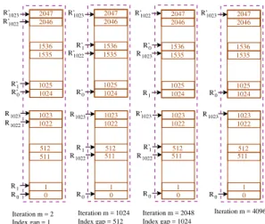
NTT has a complex memory access pattern due to loop-dependent index gap between the two coefficients that are processed in the butterfly steps (see Alg. 1). When parallel butterfly cores are used, memory access pattern becomes even more complex and this might lead to memory access conflicts; e.g., two cores are trying to read or write simultaneously in the same BRAM. Furthermore, if the two coefficientsA[k+j] andA[k+ j+m/2] in line 9 and 10 of Alg. 1 reside in the same BRAM, then their reads must be performed sequentially over the single read port. Hence, a special memory access scheme is needed to tackle these two issues. In [20] a single core memory-efficient NTT algorithm was constructed that overcomes the second bottleneck by keeping the two required coefficients (A[k+j] andA[k+ j+m/2]) together in a same word of the memory. Thus, a single read operation brings the paired coefficients to the arithmetic unit. In our implementation we store the paired coefficients in the same memory word [30] and construct a dual core NTT algorithm that overcomes the first bottleneck, i.e., access conflict.As two coefficients are stored in the same word, the virtual depth of the memory becomes 2048 and the virtual word size becomes 60 bits. The memory unit is composed of two blocks (vertical brown rectangles in Fig. 3), each containing 1024 words of 60-bit size. The lower block is accessed for the address range 0 to 1023 and the upper block is accessed for the address range 1024 to 2047. Within each brown block, two BRAM36Ks are aligned, i.e., they have a common read address bus, a common write address bus and a common write enable signal. These brown blocks can be accessed in parallel. The pattern of memory reads during the execution of our dual core NTT algorithm is shown in Fig. 3. Write operations during NTT have the same pattern, and hence they are not shown in the figure. Read requests by the first and the second butterfly cores are indicated usingRandR0 respectively with the sequence numbers. The access pattern changes depending on the outer-most loop variablem in Alg. 1.
Fromm= 2 (start of NTT) till m= 1024, the maxi-mum index-gap between two consecutive read/write ad-dresses is 512. Hence, the memory adad-dresses requested by the first and the second butterfly cores are exclusively within the ranges [0, 1023] and [1024, 2047] respectively. Naturally, the first core reads/writes the lower memory block and the other core reads/writes the upper memory block without causing any conflict.
R0 R1 R1022 R1023 R’0 R’1 R0 R1 R1022 R1023 R’0 R’1 R’1022 R’1023 R’1022 R’1023 R0 R1 R1022 R1023 R’0 R’1 R’1022 R’1023 Iteration m = 1024 Index gap = 512 Iteration m = 2048 Index gap = 1024 R0 R1023 R’0 R’1023 Iteration m = 4096 2047 2046 1536 1535 1025 1024 1 1022 512 0 1023 1 1022 512 0 1023 511 2047 2046 1536 1535 1025 1024 2047 2046 1536 1535 1025 1024 1 1022 512 0 1023 511 1 1022 512 0 1023 511 2047 2046 1536 1535 1025 1024 Index gap = 1 Iteration m = 2 511
Figure 3: Memory access during two-core NTT.
For m = 2048, the index-gap is 1024. As a conse-quence, each core now reads/writes both memory blocks. We eliminate memory access conflicts by inverting the order of address requests generated by the second core. This is explained as follows. The first core reads ad-dresses in the sequence 0 (lower memory block), 1024 (upper memory block), 1 (lower memory block), 1025 (upper memory block), and so on; whereas the other core reads addresses in the sequence 1536 (upper memory block), 512 (lower memory block), 1537 (upper mem-ory block), 513 (lower memmem-ory block), and so on. The first sequence accesses the lower memory first whereas the second sequence accesses the other. This allocation avoids memory access conflicts.
The last loop in the NTT (m = 4096) is executed ‘one memory word at a time’ following [30] and hence the two cores exclusive read/write the lower and upper memory blocks respectively.
5.1.4
Architecture of NTT core
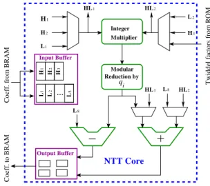
Our NTT algorithm applies parallel processing on top of the single thread memory-efficient NTT algorithm pre-sented by Roy et al. [30], so our architecture for the NTT computation has some similarities with their architec-ture. One difference is that [30] designs the architecture for computing public-key encryption where the polyno-mials are typically 256 or 512 coefficients long. Since our target is to speedup homomorphic multiplications, where polynomials are much larger, instead of comput-ing the constant twiddle factors, we store them uscomput-ing on-chip memory to save cycles. This decision also elim-inates bubble-cycles in the pipeline data-path of NTT computation. Pipeline bubbles are caused due to the data dependencies of the butterfly steps on the twiddle factors. Previous work [20] reports that 20% cycles are lost as bubble-cycles during NTT computation. Hence, our choice of storing the twiddle factors is a logical for speeding up the slow homomorphic multiplication.
In Fig. 4 we show the architecture diagram of a single NTT arithmetic core. The integer multiplier is a 30x30 multiplier, implemented using DSP slices. The result from the multiplier, which is a 60 bit integer, is reduced
1 H H2 L1 L8 L2 H3 HL1 HL2 HL1 L8 HL2 H 1 H 2 H 3 L 2 L 1 . .. L 8 q i Input Buffer Output Buffer Integer Multiplier NTT Core
Coeff. from BRAM
Coeff. to BRAM
Twiddel factors from ROM
Modular Reduction by
Figure 4: Architecture of NTT Core.
by a primeqi using the modular reduction block.
Among all the computation blocks in Fig.4, the mod-ular reduction circuit is the costliest one. It can be designed in several ways and selection of the right algo-rithm is a key to the best performance. In our imple-mentation, each NTT core should support arithmetic modulo two primes as explained in Sec. 5.1.1. Hence, we need a ‘generic’ modular reduction algorithm. ‘Bar-rett reduction’ [31] is one such algorithm and is used in [20]. However a Barrett reduction circuit is costly as it requires computation of several multiplications.
In our implementation we use a sliding window method that reduces the input integer step-by-step. With a sliding window size of 6-bits, a table called ‘reduction table’ containing 64 integersw·230 modqiforw= 0 to
w= 63 is used. At a time, the sliding window selects the most significant 6 bits of operand integer and reduces them with the help of the reduction table. This iterative process continues until the intermediate result becomes a 31-bit integer. Obtaining the final reduced result might require a subtraction ofqi or 2qi from the intermediate
result. In our implementation, these sequential steps are fully unrolled to achieve a bit-parallel modular reduction. Pipeline registers are inserted in between several of these steps to achieve a high clock frequency.
A pipeline strategy is also applied in the other arith-metic circuits (multiplier, adder and subtractor). The pipelined circuits are shown in green border in Fig. 4.
5.2
Architecture of
Liftq→QIn Sec. 4.3 we described two ways to compute the
Liftq→Q. We implement architectures for both ways.
5.2.1
Architecture for traditional
Liftq→QThe first architecture uses long integer arithmetic and follows the design methodology presented in [20]. The flow of sequential and parallel computation steps is shown using block diagrams in Fig. 5. Long integer arithmetic is performed in the lower two blocks that compute sop and division by q respectively. Though shown in the flow diagram, the constant computations
a’12 a’6 . . . q*i q i ~ q 6 0 5 ai. . mod q*i q i ~ q12 ... 6 6 6 6 a = a’ − v’ mod q 12 a = a’ − v’ mod q12 12 12 q*i q~i sop = 0 5 ai. . sop q v = v’ = v’ q mod q. 6 6 v’ = v’ q mod q. 12 12 ... = = 0 5 ai. . mod Block 1
Block 2 Block 3 Block 4
Block 5
Figure 5: Architecture of Lift q→Q using
multi-precision arithmetic.
such as ˜qi·q∗i are not performed in the actual
implemen-tation as these values are stored in tables to minimize the time requirement. Following [20] the division byqis performed by multiplyingsop with the reciprocal ofq.
We apply a block-level pipeline strategy to improve throughput. In such an architecture, the maximum throughput is determined by the slowest component in the pipeline processing. The division block is the slowest among all blocks and hence it determines the throughput. Other blocks in the Fig. 5 have been designed to match the throughput of the division block.
5.2.2
Architecture for new HPS [29]
Liftq→QWe propose the first hardware implementation of
Liftq→Q using the new HPS [29] method that does not
perform long integer arithmetic. The flow of its sequen-tial and parallel steps are identified in Fig. 6. From the flow diagram we see that the best processing time can be obtained if all the blocks are computed in pipeline. Hence, we implement a block-level pipeline architecture and achieve high-level parallel processing.
The HPS optimization replaces costly long-integer arithmetic by multiple small-integer operations. This gives us the opportunity to introduce additional within-blockparallel processing. We design the individual blocks to have a processing time of seven cycles at most, since the output is a set of seven residues. ‘Block 2’ is the most expensive since it computes seven summation-of-products, where each summation involves six products. Hence to speedup ‘Block 2’, we keep seven parallel Multiply-and-Accumulate (MAC) circuits in it.
The other blocks have less computation load and hence they process the input operands sequentially. For e.g., ‘Block 1’ multiplies the inputais byqis one by one taking
six cycles; the last block computing the result residues one by one in total seven cycles.
In ‘Block 3’ the divisions byqis are performed. The
original HPS paper [29] uses floating point divisions for
a’6= . . . 0 5 mod q6 * a’i.qi 0 5 mod q12 * a’i.qi a’12= a’i (1/q ) i v’ = v’ q mod q. 6 6 v’ = v’ q mod q12 . 12 ... . = a’0 a ~0q0mod q0 . = a’5 a ~5q5mod q5 ... v’ = 0 5 . . . . a = a’ − v’ mod q 12 a = a’ − v’ mod q12 6 6 6 6 12 12 Block 1 Block 2 Block 3 Block 4 Block 5
Figure 6: Architecture of Lift q→Q using small
this purpose. We do not use any costly floating point unit and compute the divisions as multiplications by the reciprocals 1/qi. This leads to simplified architecture and
faster processing. The constant reciprocals are stored in the ROM memory with a precision of 89-bits after the decimal point. Actually the first 29 bits after the decimal point in each reciprocal 1/qi are all-zeros. Hence, the
multiplications are actually computed between 30-bit a0is and 60 non-zero bits of 1/qis. The probability of
getting an approximation error in this way is less than 2−80, whereas it is 2−53 in the original HPS paper [29].
Integer Multiplier Integer Adder qj Modular Reduction by acc constants coefficients
Figure 7: Generic architecture for multiplication based building blocks used in Fig. 6.
Fig. 7 shows a generic architecture for the building blocks used in Fig. 6 to multiply with or without lation. Two optional data-paths with or without accumu-lation are shown in blue and red color respectively. The constants are kept in on-chip memory. We also apply low-level pipeline strategy to improve the clock frequency of the basic arithmetic circuits namely, integer multi-plier, modular reduction, modular adder/subtractor etc. In this way, two levels of pipeline strategies (i.e., block and low-level) are applied to achieve the best perfor-mance. Buffer registers are placed in between blocks when needed for synchronizing the flow of computation.
5.3
Architecture of
ScaleQ→qWe describe two architectures to implement the
ScaleQ→q operation. The first architecture uses
multi-precision arithmetic and follows the design methodology of [20]. The flow of sequential and parallel computation steps is shown in Fig. 8. ‘Block 3’ is the costliest, com-puting division byq. Here tis the plaintext modulus (e.g., 2 for binary messages). Again, the division is per-formed by multiplying the dividend by the reciprocal of q. Since,ais 390 bit large, the precision of the reciprocal should be larger than 571. Note that division byqis also performed in Fig. 5 during theLiftq→Q operation. Since
Liftq→Q andScaleQ→q are not computed simultaneously,
the division architecture is resource-shared by the both operations. The cycle count of the division operation during ScaleQ→q is almost four times larger than the
division operation duringLiftq→Q as the precision of the
reciprocal and the width of the dividend both are two times larger. The other blocks have been designed to have similar cycle count as Block 3. We apply block-level pipeline strategy to increase the throughput.
Now we propose the first hardware implementation of
ScaleQ→q using the HPS [29] method. The flow of its
sequential and parallel steps are identified in Fig. 9. Sim-ilar to the previous optimizedLiftq→Q architecture, we
apply block-level pipeline strategy to achieve high-level parallelism. ‘Block 1’ and ‘Block 2’ compute summa-tion of products using MAC circuits (without modular
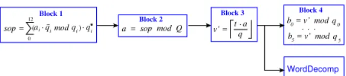
qi ~ qi q*i a = sop mod Q Block 2 t a q . v’ = Block 3 q 0 b = v’ mod 0 ... q 5 b = v’ mod 5 Block 4 = . 0 12 i a mod ( (. sop Block 1 WordDecomp
Figure 8: Architecture of ScaleQ→q using
multi-precision arithmetic. sop =R ai.R i 0 5 i a Ii sop =I p q v’ =j t Q qj j qj . 0 5 for j=6 to j=12 RNS Block 1 Block 2 Block 3 Block 4 Block 5 R for j=6 to j=12 j I j a’ =aj. mod j sop + sop + a’ mod q
Figure 9: Architecture of Scale Q→q using small
number arithmetic.
reduction in Fig. 7). The constants Ii andRi in these
two blocks stand for the integer and real parts of the constants tQ˜ip
qi respectively. The realsRiare stored with
60-bit precision after the decimal point. ‘Block 3’ uses the circuit of Fig. 7 with the red data-path. The final block in the flow diagram receives seven residues in the RNS of p. It then reuses the Liftq→Q architecture of
Fig. 6 to compute the residues in the RNS representa-tion of q. As the block-level pipelined architecture of Fig. 6 computes in seven cycles, the remaining blocks of theScaleQ→q architecture in Fig. 9 have been designed
to compute in seven cycles.
Since several of the building blocks in theLiftq→Qand
ScaleQ→q architectures use ‘multiplication and
accumu-lation’ type operations, one design option is to realize a resource-shared architecture so that the similar or somewhat similar operations can be executed. This ap-proach would reduce the area requirement and increase the computation time significantly. In our architecture we keep the building blocks separate to apply block-level pipeline processing.
Block diagram of the instruction-set coprocessor show-ing the connections of the seven RPAUs, two parallel cores for Liftq→Q and ScaleQ→q and the memory file
Figure 10: Block diagram of coprocessor for com-puting homomorphic operations
Application 0 ARM Core Application 1 ARM Core Networking ARM Core Memory Controller DMA Interfacing Unit Interfacing Unit Coprocessor 1 Coprocessor 0 Processing System Programmable Logic
Figure 11: The high-level architecture and inter-facing of hardware and software
(shown using rectangles M) is shown in Fig. 10.
5.4
Hardware Software Interface
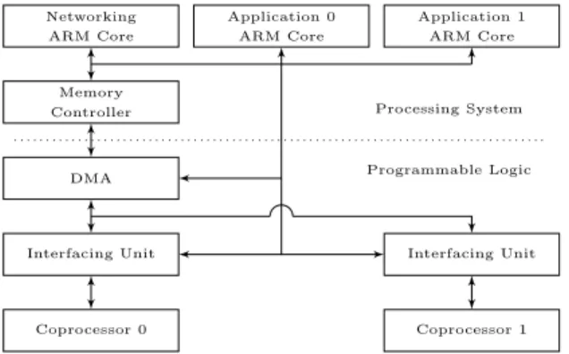
The high-level architecture of our HW/SW codesign is shown in Fig. 11. We enable parallel processing with two coprocessor instances in the FPGA, and reserve one Arm core for each. We also used a third Arm core for managing the network connection to clients, and distributing the work load among the application cores.
Our software runs ‘baremetal’ i.e. without any oper-ating system, and useslight-weight IP stack for client-server communication. For the data transfer between the DDR memory and hardware, it uses Direct Memory Access (DMA) placed between the memory and inter-facing units shown in Fig. 11. The hardware could also access the DDR memory for intermediate computation results, but that would add a significant data transfer overhead. Hence, BRAM-based on-chip memory is used.
In the software side, we apply efficient memory man-agement. The coefficients of a ciphertext are kept in contiguous memory locations. Using this strategy, we could transfer large data very fast in a continuous DMA. In Sec. 6 we will show that the use of this strategy indeed reduces the data transfer overhead significantly.
Working with parallel executing cores increases the performance significantly in both software and hardware, but also requires a complex design as it requires access synchronization. The ‘Networking Arm Core’ in Fig. 11 is chosen to manage the DDR memory allocation. DMA access conflicts, i.e., two simultaneous DMA requests, are avoided using Xilinx’ mutual exclusion HW IP Core.
6.
RESULTS
We implemented our domain specific programmable accelerator for homomorphic computations on ciphertext on a single Xilinx Zynq UltraScale+ MPSoC ZCU102 Evaluation Kit [24]. We coded the software inCand com-piled it withGCC(available through the Xilinx SDK). Our custom hardware modules were described with Ver-ilog. During design-space exploration, we implemented two hardware architectures. One of them uses traditional CRT-basedLiftq→Q and ScaleQ→q operations,
perform-ing multi-precision integer arithmetic. The other applies
Table 1: Performance of high-level operations using one coprocessor.
Operation Speed
(cycles) (msec)
Multin HW 5,349,567 4.458
Addin HW 31,339 0.026
Addin SW 54,680,467 45.567
Send two ciphertexts to HW 434,013 0.362
Receive result ciphertext from HW 215,697 0.180
the HPS optimization techniques [29] and achieves the best performance. From now on, if not exclusively men-tioned, performance and area reports are presented only for the faster architecture. Results for the slower are presented briefly in a subsection.
6.1
Timing results
The hardware-based coprocessor runs at 200 MHz and the Arm processors run at 1.2 GHz. The DMA module is clocked at 250 MHz, aiming to minimize the data transfer overhead. Cycle counts for various opera-tions are measured from the software side reading the Arm processors’ cycle-count register. As our coprocessor implements an instruction-set architecture, we report timing requirements for high-level operations and the low-level instructions used for them. In Table 1 perfor-mances of the high-level operations are presented. The timings forAddand Multin HW exclude the overhead of transferring the operand and result ciphertexts. Com-puting the simpleAddoperation in SW using a single Arm core requires 80 times more time than the same computation in HW, including the overhead of sending and receiving ciphertexts. The computation time for
Multincludes the overhead of intermediate data trans-fers (roughly 30%) during the relinearization steps. If larger FPGAs are used, this overhead could be reduced or eliminated by storing the relinearization keys in the HW at the cost of additional ROM memory.
In our FPGA we place two coprocessors in parallel and achieve 2x throughput. E.g, two Mult operations take roughly the same time as oneMultoperation. We can compute 400 Multoperations per second.
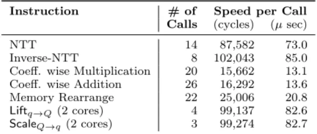
The performance of each instruction of our instruction-set architecture is shown in Table 2. The table also shows how many times each instruction is called for computing one Mult operation. TheAdd operation requires exe-cuting the Coefficient-wise-Addition instruction twice as a ciphertext in the FV scheme is composed of two polynomials inRq. TheLiftq→Q instruction lifts a
poly-nomial from Rq to RQ in less than 0.1ms, using two
parallel cores. TheScaleQ→q instruction first scales the
input polynomial and computes the intermediate re-sult in the RNS of p. Then it uses the data-path of
Liftq→Q to map this result to the RNS representation
ofq. Hence,ScaleQ→q performs more computation than
Liftq→Q. But, benefiting the block-level pipeline strategy
in the sequential execution of the two steps, the overall computation time forScaleQ→q remains almost equal to
Table 2: Performance of individual instructions.
Instruction # of Speed per Call
Calls (cycles) (µsec)
NTT 14 87,582 73.0
Inverse-NTT 8 102,043 85.0
Coeff. wise Multiplication 20 15,662 13.1
Coeff. wise Addition 26 16,292 13.6
Memory Rearrange 22 25,006 20.8
Liftq→Q(2 cores) 4 99,137 82.6
ScaleQ→q(2 cores) 3 99,274 82.7
Table 3: Comparison of data transfer techniques.
Data Transfer Type Speed
(cycles) (µsec)
Single Transfer of 98,304-bytes 90708 76
Transfers with 16,384-byte chunks 130686 109
Transfers with 1,024-byte chunks 242771 202
We put significant effort in minimizing the overhead of data transfer. The first decision we took was to keep enough internal memory to avoid frequent access to the external DDR memory during the execution of Mult. Only during the relinearization steps, data transfer is needed to load the large relinearization keys. The second decision is using the optimum data transfer size, as mentioned in Sec. 5.4. In Table 3 costs for three types of data transfers are shown. In our implementation, we use single transfer to achieve the minimum overhead.
6.2
Resource Requirements
Table 4 shows the resource utilization in the target FPGA. It shows that the design is constrained on mem-ory size. Besides the two coprocessors, the DMA and Interfacing Unit contributes to utilization. On the soft-ware side, three Arm cores of the target Zynq are used.
6.3
Performance without HPS optimization
The other coprocessor architecture uses slowerLiftq→Q
andScaleQ→q architectures. At 225 MHz clock, using
only one core we can compute theLiftq→QandScaleQ→q
operations in 1.68 and 4.3 msec respectively. To speedup computation, we keep four parallel cores for computing
Liftq→Q andScaleQ→q. The polynomial arithmetic unit
in the faster and slower architectures are similar. At 225 MHz clock frequency, this coprocessor architecture requires 8.3 msec (including all data transfer overhead) to compute one Mult operation. Though the Liftq→Q
Table 4: Resource Utilization
(for Zynq UltraScale+ ZCU102 Evaluation Kit)
LUTs Registers BRAMs DSPs
(# of used instances) (% utilization)
Overall 13369249% 6031211% 89%815 16%416
Single 63522 25622 388 208
Coprocessor 23% 5% 43% 8%
Table 5: Estimated results for different parame-ter sets considering a single processor.
Parameter Resources Multtime
(n,logq) LUT/Reg./BRAM/DSP Comp./Comm./Total
212,180 64K/25K/0.4K/0.2K 4.46/0.54/5.0 msec
213,360 128K/50K/1.6K/0.4K 9.68/2.16/11.9 msec
214,720 256K/100K/6.4K/0.8K 21.0/8.64/29.6 msec
215,1,440 512K/200K/25.6K/1.6K 45.6/34.6/80.2 msec
andScaleQ→q are much slower, the time forMult is less
than 2x slower in comparison to the faster coprocessor architecture. This difference is due to a difference in the relinearization operation. In the faster architecture, each relinearization key is a vector of six polynomials. Traditional CRT-basedScaleQ→q offers the flexibility to
choosing the number of polynomials in the relineariza-tion key. The slower coprocessor uses three times smaller relinearization key in comparison to the faster architec-ture. If both use relinearization keys of length six, then the slower processor would become another 30% slower.
We measures the power consumption of our design using the Power Advantage Tool. The static power consumption is 5.3 W. The continuous execution of a ho-momorphic multiplication operation including the input and output data transfers requires 2.2W dynamic power consumption on a single core execution. In the concur-rent double core execution of the same, the dynamic power consumption reaches 3.4W.
6.4
Estimates for other parameter sets
For estimating performance for larger parameter sets, we assume that the sizes of target FPGAs also scale appropriately. We assume that for every doubling of both the polynomial degree and coefficient size (≈4.34×
increase in overall computation) in the parameter set, we double the number of RPAUs and Lift/Scale cores (≈ 2× increase in logic-area). Consequently, the net computation increases by ≈ 2.17×. The overhead of off-chip data transfer increases by ≈4×. In Table 5 we apply this estimation model iteratively to estimate area, memory and performances for various parameter sets.
6.5
Comparisons with Related Works
In the literature there are several reported implemen-tations of somewhat homomorphic encryption (SHE) schemes. A totally fair comparison between the imple-mentations is not always possible, firstly because there are several SHE schemes, secondly because there are differences in the choice of parameters, and finally be-cause the implementation platforms vary. The most fair comparison is with the NFLlib [22] based software mentation of the FV scheme presented in [4]. The imple-mentation uses a similar parameter set. The highly op-timized single threaded software implementation spends 33 milliseconds and 0.1 milliseconds for computing one
Mult andAddrespectively on an Intel Core i5-3427 pro-cessor running at 1.8 GHz. Using two copropro-cessors in the FPGA, we achieve more than 13x throughput with respect to the NFLlib-based software implementation.
Latest generation Intel i5 reaches up to 40W on heavy load operations [32]. In comparison, our processor has a peak power consumption of 8.7 W.
A very recent implementation [33] by Badawi et al. presents performances of the FV scheme for various parameter sets on CPUs and GPUs. They also use HPS optimization for fasterLiftq→Q andScaleQ→q
oper-ations. Their single-threaded software implementation for a parameter set n = 4096 and 60-bit q requires around 10 msec to compute one homomorphic multi-plication for 30-bit moduli size (which we also use) on Intel(R) Xeon(R) Platinum running at 2.1 GHz. Using 26 threads in multi-threaded experiments, they could reduce the time to 4 msec only. Their highly optimized GPU implementations on Tesla K80 (2496 cores, 0.82 GHz, 12 GB RAM) and Tesla V100 (5120 cores, 1.38 GHz, 16 GB RAM) require 1.98 and 0.86 msec respec-tively at the cost of humongous power consumption. We estimate that for 180-bitq, computation times of their implementations would increase at least three times. In a fair comparison (i.e.,n= 4096 and 180-bitq), their fastest implementation on Tesla V100 performing 388 homomorphic multiplications per second is slower than our implementation achieving 400 multiplications.
P¨oppelmann et al. [14] implemented of the YASHE [8] scheme in the Catapult [34] architecture which is an FPGA-based domain specific accelerator for cloud com-puting applications. Their implementation for the pa-rameter set with polynomial size of 4,096 (same as ours) and ciphertext coefficient size 128 bits (smaller than ours) run at 100 MHz clock frequency and require 6.75 msec. The YASHE scheme is computationally three to four times faster than the FV scheme and has roughly half memory requirement. Even with a faster SHE scheme and a smaller parameter set, their implementation is slower than ours. Achieving two times higher clock fre-quency (200 MHz) as well as computation using parallel coprocessor cores are major advancements towards mak-ing homomorphic encryption practical. The YASHE scheme is not considered secure anymore and hence is not used due to an attack by Albrecht et al. [35] in 2016.
Next we compare our results with the hardware im-plementation by Roy et al. [20]. They implement the FV scheme for a much larger parameter set (polynomial size 32,768 and ciphertext coefficient size 1,228 bits). Due to such a large parameter set, only one residue polynomial arithmetic unit could fit in their target plat-form that has a medium size Xilinx Virtex 6 FPGA. Their architecture suffers from a massive data transfer overhead as they need to continuously read and write DDR memory. We designed our programmable archi-tecture for supporting less complex cloud computing applications (thus smaller parameter set). We use suf-ficient on-chip memory (implemented using BRAMs) to store the two operand ciphertexts and in this way we minimize data transfer overhead. We estimate that a hypothetical architecture following our design steps (explained in Sec. 6.4) would be able to compute ho-momorphic multiplication in less than 0.1 sec (Table 5) when implemented on a sufficiently large FPGA. This
significant difference is mostly due to the fact that our design methodology avoids costly long integer arithmetic and frequent off-chip data transfer and at the same time applies more parallel processing.
7.
CONCLUSIONS
In this paper we presented a programmable and high-performance domain specific architecture for computing homomorphic operations on ciphertext. We applied the recent arithmetic optimization techniques proposed by Halevi, Polyakov and Shoup to avoid costly multi-precision arithmetic, and designed a parallel polynomial multiplication algorithm with an efficient memory access scheme to speedup the homomorphic multiplication op-eration. In the hardware architecture, we used parallel computation cores to minimize cycle count, and applied circuit-level and block-level pipeline strategy to benefit parallel processing and reach a clock frequency of 200 MHz. Further, we utilized the on-chip memory opti-mally to avoid frequent off-chip data transfers. Using highly optimized building blocks, we constructed our multi-core multi-processor architecture. Finally we im-plemented our optimized domain specific programmable architecture on a single Xilinx Zynq UltraScale+ MP-SoC ZCU102 Evaluation Kit and demonstrated that it can achieve a throughput of 400 homomorphic multipli-cations per second, which is 13x faster than a heavily optimized software implementation on an Intel i5 proces-sor. Our results make homomorphic encryption practical in several cloud computing applications.
Discussions. FPGAs are becoming more and more popular in cloud computing applications. The Amazon offers FPGA-accelerated cloud for accelerating perfor-mance critical applications [36]. An Amazon EC2 F1 instance offers either one or eight Xilinx Virtex Ultra-Scale+ FPGAs attached to a server-grade Intel Xeon processor. These FPGAs have five times more resources than our Zynq platform. Our instruction-set coproces-sor architecture has a very modular structure. Most of the building blocks, excluding the IP Cores, have been described using behavioral Verilog. Hence, the source codes of our accelerator can be easily ported to these powerful FPGAs. We estimate that each Amazon F1 instance could run at least ten coprocessors in parallel. Our coprocessor architecture offers trade-offs between hardware cost and performance. Therefore, we would like to remark that the utilization and performance re-sults reported in this paper are not the definite numbers, but only belongs to the configuration used in this paper. The design decisions can be tweaked to meet different requirements. For e.g., by using more computation cores we could achieve a lower latency or by reducing the number of memories we could lower the hardware cost.
8.
ACKNOWLEDGEMENTS
This work was supported in part by the Research Council KU Leuven: C16/15/058. In addition, this work was supported by the European Commission through the Horizon 2020 research and innovation programme under grant agreement Cathedral ERC Advanced Grant
695305, by H2020-ICT-2014-644209 HEAT, by EU H2020 project FENTEC (Grant No. 780108) and by the Hercules Foundation AKUL/11/19.
9.
REFERENCES
[1] IBM, “Top 7 most common uses of cloud computing,” 2014.
https://www.ibm.com/blogs/cloud-computing/2014/02/ 06/top-7-most-common-uses-of-cloud-computing. [2] J. W. Bos, K. Lauter, and M. Naehrig, “Private predictive
analysis on encrypted medical data,”Journal of Biomedical
Informatics, 2014.
[3] N. Peng, G. Luo, K. Qin, and A. Chen, “Query-biased
preview over outsourced and encrypted data,”Scientific
World Journal, 2013.
[4] J. W. Bos, W. Castryck, I. Iliashenko, and F. Vercauteren, “Privacy-friendly forecasting for the smart grid using
homomorphic encryption and the group method of data
handling,” inProgress in Cryptology - AFRICACRYPT
2017, 2017.
[5] T. Graepel, K. Lauter, and M. Naehrig, “Ml confidential:
Machine learning on encrypted data,” inInformation
Security and Cryptology – ICISC 2012, 2012.
[6] R. L. Rivest, L. Adleman, and M. L. Dertouzos, “On data
banks and privacy homomorphisms,”Foundations of secure
computation, 1978.
[7] C. Gentry, “Fully homomorphic encryption using ideal
lattices,” inProceedings of the 41st ACM Symposium on
Theory of Computing (STOC 2009), pp. 169–178, 2009. [8] J. W. Bos, K. Lauter, J. Loftus, and M. Naehrig, “Improved
security for a ring-based fully homomorphic encryption
scheme,” inProceedings of the 14th IMA International
Conference on Cryptography and Coding (IMACC 2013), 2013.
[9] J. Fan and F. Vercauteren, “Somewhat practical fully homomorphic encryption.” Cryptology ePrint Archive,
Report 2012/144, 2012.http://eprint.iacr.org/.
[10] A. Badawi, B. Veeravalli, C. Mun, and K. Aung,
“High-performance FV somewhat homomorphic encryption
on GPUs: An implementation using CUDA,”IACR
Transactions on Cryptographic Hardware and Embedded Systems, 2018.
[11] W. Wang and X. Huang, “FPGA implementation of a large-number multiplier for fully homomorphic encryption,” inIEEE International Symposium on Circuits and Systems (ISCAS 2013), 2013.
[12] Y. Dor¨oz, E. ¨Ozt¨urk, and B. Sunar, “Evaluating the
hardware performance of a million-bit multiplier,” in Proceedings of the 16th Euromicro Conference on Digital System Design (DSD 2013), 2013.
[13] W. Wang and X. Huang, “VLSI design of a large-number
multiplier for fully homomorphic encryption,”IEEE
Transactions on Very Large Scale Integration (VLSI) Systems, 2014.
[14] T. P¨oppelmann, M. Naehrig, A. Putnam, and A. Macias,
“Accelerating homomorphic evaluation on reconfigurable
hardware,” inCryptographic Hardware and Embedded
Systems - CHES, 2015.
[15] X. Cao, C. Moore, M. O’Neill, E. O’Sullivan, and N. Hanley, “Optimised multiplication architectures for accelerating fully
homomorphic encryption,”IEEE Transactions on
Computers, 2016.
[16] D. Cousins, K. Rohloff, and D. Sumorok, “Designing an FPGA-accelerated homomorphic encryption co-processor,” IEEE Transactions on Emerging Topics in Computing, to appear.
[17] E. ¨Ozt¨urk, Y. Dor¨oz, E. Sava¸s, and B. Sunar, “A custom
accelerator for homomorphic encryption applications,”IEEE
Transactions on Computers, 2017.
[18] Y. Dor¨oz, E. ¨Ozt¨urk, E. Savas, and B. Sunar, “Accelerating
LTV based homomorphic encryption in reconfigurable
hardware,” inCryptographic Hardware and Embedded
Systems - CHES, 2015.
[19] S. S. Roy, K. J¨arvinen, F. Vercauteren, V. Dimitrov, and
I. Verbauwhede, “Modular hardware architecture for somewhat homomorphic function evaluation,” in Cryptographic Hardware and Embedded Systems - CHES, 2015.
[20] S. S. Roy, K. J¨arvinen, J. Vliegen, F. Vercauteren, and
I. Verbauwhede, “HEPCloud: An FPGA-based multicore processor for FV somewhat homomorphic function
evaluation,”IEEE Transactions on Computers, 2018.
[21] V. Migliore, M. M. Real, V. Lapotre, A. Tisserand, C. Fontaine, and G. Gogniat, “Hardware/software co-design of an accelerator for FV homomorphic encryption scheme
using Karatsuba algorithm,”IEEE Transactions on
Computers, 2018.
[22] CryptoExperts, “FV-NFLlib,” 2016.
https://github.com/CryptoExperts/FV-NFLlib. [23] M. Research, “Simple Encrypted Arithmetic Library
(SEAL),” 2016.
https://www.microsoft.com/en-us/download/details.aspx?id=56202.
[24] Xilinx,ZCU102 Evaluation Board User Guide, 2017. v1.3.
[25] C. Dobraunig, M. Eichlseder, L. Grassi, V. Lallemand, G. Leander, E. List, F. Mendel, and C. Rechberger, “Rasta: A cipher with low ANDdepth and few ANDs per bit,” 2018.
https://eprint.iacr.org/2018/181.
[26] M. R. Albrecht, “Complexity estimates for solving LWE.”
https://bitbucket.org/malb/lwe-estimator/raw/HEAD/estimator.py.
[27] D. Bernstein, “Fast multiplication and its applications,” Algorithmic Number Theory, 2008.
[28] T. H. Cormen, C. Stein, R. L. Rivest, and C. E. Leiserson, Introduction to Algorithms. McGraw-Hill Higher Education, 2001.
[29] S. Halevi, Y. Polyakov, and V. Shoup, “An improved RNS variant of the BFV homomorphic encryption scheme,” 2018.
https://eprint.iacr.org/2018/117.
[30] S. Sinha Roy, F. Vercauteren, N. Mentens, D. D. Chen, and I. Verbauwhede, “Compact ring-LWE cryptoprocessor,” in Cryptographic Hardware and Embedded Systems ˆa ˘A¸S CHES
2014, Springer Berlin Heidelberg, 2014.
[31] P. Barrett, “Implementing the Rivest Shamir and Adleman public key encryption algorithm on a standard digital signal
processor,” inAdvances in Cryptology — CRYPTO’ 86:
Proceedings, 1987.
[32] “Intel Kaby Lake Core i7-7700K, i7-7700, i5-7600K, i5-7600 Review.” URL:
www.tomshardware.com/reviews/intel-kaby-lake-core-i7-7700k-i7-7700-i5-7600k-i5-7600,4870-10.html, last checked on 2018-08-15, 2017.
[33] A. A. Badawi, Y. Polyakov, K. M. M. Aung, B. Veeravalli, and K. Rohloff, “Implementation and performance evaluation of RNS variants of the BFV homomorphic encryption
scheme,” 2018.https://eprint.iacr.org/2018/589.
[34] A. P.et al., “A reconfigurable fabric for accelerating
large-scale datacenter services,” in2014 ACM/IEEE 41st
International Symposium on Computer Architecture (ISCA), 2014.
[35] L. D. Martin Albrecht, Shi Bai, “A subfield lattice attack on overstretched NTRU assumptions: Cryptanalysis of some FHE and Graded Encoding Schemes,” 2016.
http://eprint.iacr.org/2016/127.
[36] A. W. Instances, “Amazon EC2 F1 Instances.” URL:
https://aws.amazon.com/ec2/instance-types/f1/, last checked on 2018-08-03.