TECHNIQUES IN INTEGRATED CIRCUITS FOR
BIOSENSING, COMMUNICATION AND RADAR
Thesis by Hua Wang
In Partial Fulfillment of the Requirements for the degree of
Doctor of Philosophy
CALIFORNIA INSTITUTE OF TECHNOLOGY
Pasadena, California 2009
2009 Hua Wang
Acknowledgements
First and foremost, I would like to express my deepest gratitude to my advisor, Professor Ali Hajimiri for his support over the course of my Ph.D. study at Caltech. His high-level guidance and insightful technical advice have led me through this adventurous academic journey full of discovery. More importantly, his generous mentorship has nourished me to an extent far beyond the academic matters. His enthusiasm for knowledge and his persistence for perfection have been and will continue inspiring me to strive for excellence and success in my career.
I would also like to thank my other thesis committee members: Professor Axel Scherer, Dr. Sander Weinreb, Professor Azita Emami, and Professor Changhuei Yang for their assistance and helpful comments.
I am especially indebted to Dr. Yan Chen and Mr. David Wu for being my collaborators. Their active involvements and critical contributions are essential and irreplaceable for the success of my Ph.D. project.
Jeon, Shohei Kosai, Edward Keehr, Juhwan Yoo, Kaushik Sengupta, Jay Chen, Steven Bowers, Kaushik Dasgupta and Tomoyuki Arai for their support.
I would also like to thank Michelle Chen, Carol Sosnowski, Hamdi Mani, Naveed Near-Ansari, John Lilley, Gary Waters, Kent Potter, Jim Endrizzi, Laura Flower Kim, Tess Legaspi, Linda Dozsa, Tanya Owen, Trevor Roper and Lynn Hein, whose valuable work has created a friendly environment at Caltech for students.
This research has been supported by the Office of Naval Research and Caltech Innovation Initiative (CI2) Research Grant.
I am also thankful to my supportive friends, Ali Vakili,Wen Li, Guangxi Wang, Tao Liu, Fangwei Shao, Ray Huang, Mike Liu, Jeffrey Chun-Hui Lin, Costis Sideris, Young Shik Shin, Udi Vermish, Jifeng Peng, Sawyer Fuller, Quoc (Brandon) Quach, Weiyi Li, Howard Ge and Frank Weigang Bao, who have always encouraged me.
Abstract
Today’s CMOS technology provides circuit designers with a powerful implementation platform that supports innovation opportunities on both circuit-topology and system-architecture levels. Moreover, the versatility of CMOS implementation opens the door for a plethora of challenging and exciting interdisciplinary research.
This dissertation focuses on investigating novel techniques and applications for precision frequency and phase synthesis in CMOS. It consists of two parts: a CMOS compatible molecular-level biosensor and a multiple-beam/multi-band scalable CMOS phased array receiver system.
In the first part, a frequency-shift-based magnetic biosensing scheme is introduced to address the Point-of-Care (PoC) biomolecular diagnosis which requires high-sensitivity, ultra-portability and low-cost. Compared with existing biosensing schemes, the proposed scheme achieves a competitive sensitivity without using optical devices, external biasing fields or expensive post-processing steps. A discrete implementation first verifies the sensing mechanism and reveals several design insights. An integrated implementation based on standard 130nm CMOS process is then designed with differential sensing and temperature controlling schemes. Overall, with a differential uncertainty of 0.13ppm for relative frequency shift, the sensor achieves reliable detection of one single micron-size magnetic particle (D=4.5μm, 2.4μm and 1μm) as well as 1n-Molar real DNA samples labeled by magnetic nanoparticles (D=50nm).
Contents
Acknowledgement iv
Abstract vi
List of Figures xi
Chapter 1: Introduction
1
1.1 Organization ... 3Chapter 2: CMOS Biosensor
5
2.1 Introduction ... 52.2 A Brief Survey on CMOS Biosensor Technology ... 7
2.2.1 CMOS Fluorescent Biosensor ... 8
2.2.2 CMOS Electrochemical Biosensor ... 12
2.2.3 CMOS Magnetic Biosensor ... 16
2.3 Chapter Summary ... 20
Chapter 3: Frequency-Shift-Based Magnetic Particle
Sensing Scheme
21
3.1. Introduction ... 213.2. Frequency-Shift-Based Magnetic Sensor Mechanism ... 23
3.3. Oscillator Based Frequency-Shift Sensing ... 24
3.4. Sensor Signal Strength ... 26
3.4.1 Spatial Variation of the Sensor Transducer Gain ... 30
3.4.2 Sensor Inductor Scaling Rule ... 33
3.5 Sensor Noise Floor ... 35
3.5.1 Oscillator Phase Noise ... 36
3.6 Sensing Inductor Optimization for Maximizing Sensor Signal-to-Noise Ratio
(SNR) ... 41
3.7 Chapter Summary ... 43
Chapter 4: Frequency-Shift Magnetic Particle Sensor
Implementation 45
4.1. Introduction ... 454.2. A Discrete Magnetic Particle Sensor based on Thin-Film Technology ... 46
4.2.1 Sensor Circuit ... 47
4.2.2 Measurement Results ... 48
4.2.3 Limitation and Potential Improvement ... 53
4.3. A Fully Integrated CMOS Sensor Array with PDMS Microfluidics Sample Delivery ... 54
4.3.1 Sensor Array System Architecture ... 55
4.3.2 Sensor Core Design ... 57
4.3.3 Temperature Controller Design ... 61
4.3.4 The Low-Cost Bonding Technique to Attach PDMS Microfluidic Structures to Integrated Circuit Chip ... 64
4.3.5 Measurement Results ... 67
4.4 Chapter Summary ... 74
Chapter 5: Low Noise Techniques in Frequency-Shift
Magnetic Particle Sensor
76
5.1. Phase Noise, Jitter and Frequency Counting Window ... 775.2. Correlated Double Frequency Counting (CDFC) Technique ... 80
5.2.1 Proposed Scheme and Circuit Topology ... 81
5.2.2 A CDFC Circuit Implementation Example ... 87
5.3 Interleaving-N Correlated Double Frequency Counting and Fractional Frequency Counting ... 89
5.4 Noise Shaping Function in Correlated Double Frequency Counting ... 97
Chapter 6: Broadband Precision Phase and Amplitude
Synthesis 101
6.1. Introduction ... 101
6.2. Array Degradation due to Random Phase/Amplitude Mismatches ... 104
6.3. High-Resolution Phase/Amplitude Synthesis Scheme ... 105
6.4. A 6-to-18 GHz Dual-band Quad-beam CMOS Phased Array Receiver System .. 109
6.4.1 System Architecture ... 110
6.4.3 Phased Array Measurement Results ... 112
6.5 Chapter Summary ... 120
Chapter 7: A Broadband Active Peaking Technique 122
7.1. Introduction ... 1227.2. General Cherry-Hooper Amplifier with Active Feedback ... 125
7.2.1 General Linear Transfer Function Analysis ... 125
7.2.2 Weak Nonlinearity Performance Analysis ... 130
7.2.3 Input Referred Noise Voltage PSD ... 134
7.3. Proposed Design Method for Cherry-Hooper Amplifier with Active Feedback .. 135
7.4. Design Examples ... 143
7.4.1 A DC-19GHz Broadband Buffer Amplifier with 10dB Gain ... 144
7.4.2 A DC-12GHz Broadband Phase Rotator with a 10-Bit Resolution ... 146
7.4.3 Dual Beam-Forming Network in Phased Array with LO Phase Shifting ... 150
7.5 Chapter Summary ... 155
Chapter 8: Conclusion
157
8.1 Future Work ... 158List of Figures
Figure 2.1: Mechanism for fluorescence emission ... 9
Figure 2.2: Fluorescence spectrum for Cy3 and Alexa Fluor 610 ... 10
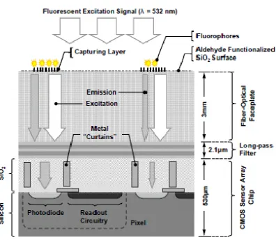
Figure 2.3: Cross section of the CMOS fluorescent-based biosensor microarray ... 11
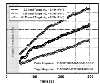
Figure 2.4: Measured real-time DNA hybridization kinetics for different concentrations .. 12
Figure 2.5: Illustration of a cyclic voltammetry experiment and description of the label-free electrochemical DNA hybridization detection principle ... 14
Figure 2.6: Measurement results for the CV electrochemical biosensor ... 15
Figure 2.7: Magnetic-label-based biosensing ... 17
Figure 2.8: SEM photo and the cross-sectional view of the GMR sensor ... 18
Figure 2.9: Measured signals for 10nM target DNA and 100nM control DNA with SEM images of particle coverage ... 19
Figure 3.1: Proposed frequency-shift-based magnetic particle sensing scheme... 23
Figure 3.2: Line-width compression effect ... 25
Figure 3.3: Spatial variation of sensor transducer gain (∆f/f0 for one 1μm magnetic bead) 30 Figure 3.4: 3D view of the stacked inductor layout ... 32
Figure 3.5: Spatial variation of sensor transducer gain for the stack inductor (∆f/f0 for one 1μm magnetic bead) ... 32
Figure 3.6: Averaged sensor transducer gain for different inductor sizes (∆L/L per 1μm bead) ... 35
Figure 3.7: Typical oscillator phase noise profile ... 36
Figure 3.8: A generic complimentary cross-coupled LC oscillator schematic with parasitic junction diodes highlighted ... 39
Figure 3.9: Averaged relative SNR for different inductors ... 42
Figure 4.1: The thin-film board used in the 1st version magnetic sensor design ... 46
Figure 4.2: The discrete sensor oscillator schematic ... 47
Figure 4.3: The experiment procedures for the dry experiment ... 48
Figure 4.4: Sensing inductors deposited with target magnetic particles ... 49
Figure 4.6: Measurement results summary on the dry experiment ... 50
Figure 4.7: PDMS microfluidic structure ... 51
Figure 4.8: Sensor module with the PDMS microfluidic device ... 51
Figure 4.9: Measurement procedures for the aqueous experiment ... 51
Figure 4.10: The delivered magnetic beads on the sensor inductor (Inductor 1) ... 52
Figure 4.11: Measurement results for summary on the aqueous experiment ... 52
Figure 4.12: The 8-cell CMOS sensor array system architecture ... 55
Figure 4.13: The effective differential inductance and its quality factor ... 58
Figure 4.14: The lateral view of the inductor EM module (not on scale) ... 58
Figure 4.15: The layout for cross-coupled pair with the NMOS pair as an example ... 59
Figure 4.16: Layout for the differential sensing oscillator pair ... 60
Figure 4.17: The generic temperature controller system schematic ... 61
Figure 4.18: The simplified schematic of the temperature controller ... 62
Figure 4.19: The layout configuration of the heater structure ... 63
Figure 4.20: The IC chip (Block 1) is immobilized onto the substrate (Block 5). Block 2 and 4 are the substrate with electrical conductive traces (Block 3). ... 64
Figure 4.21: Wire-bonds (Block 6) form electrical connections between the IC pads and the electrical conductive traces ... 65
Figure 4.22: The PDMS device (Block 7) is placed on top of the IC chip ... 65
Figure 4.23: The PDMS mixture (Part 8) is applied to surround the IC chip and the PDMS structure ... 66
Figure 4.24: CMOS magnetic sensor array chip microphotograph ... 68
Figure 4.25: The phase noise plot for sensor oscillator (measurement and simulation) ... 68
Figure 4.26: The frequency counting results with/without differential scheme ... 69
Figure 4.27: The heater response versus the on-chip temperature ... 70
Figure 4.28: The Micrograph for the CMOS chip attached with PDMS microfluidics ... 70
Figure 4.29: Typical sensor measurement results: (a) one single 2.4μm magnetic bead; (b) one single 1μm magnetic bead ... 72
Figure 4.31: Fluorescent images of test surfaces with complementary DNA and without
complementary DNA, shown on the right ... 74
Figure 5.1: Frequency counting uncertainty for normal differential sensing scheme ... 79
We name this scheme as correlated double frequency counting (CDFC) scheme. One potential circuit implementation of this CDFC scheme is shown in Figure 5.2 as follows, where T is the total counting time for one oscillator and Tset is the reset time for a practical frequency counter implementation. ... 82
Figure 5.2: One simplified circuit schematic of the proposed CDFC scheme... 82
Figure 5.3: Noise reduction factor for correlated 1/f3 and 1/f2 phase noise ... 84
Figure 5.4: Frequency uncertainty for CDFC scheme and normal differential scheme ... 86
Figure 5.5: A simplified example schematic of CDFC implementation... 88
Figure 5.6: Simulated phase noise for the example circuit ... 89
Figure 5.7: Interleaving-N CDFC scheme ... 91
Figure 5.8: Noise reduction factor for four types of noise sources ... 93
Figure 5.9: Frequency uncertainty for Interleaving-N CDFC scheme and normal differential scheme ... 94
Figure 5.10: Two fractional frequency counter implementation examples ... 95
Figure 5.11: Fractional counter operation principle ... 96
Figure 5.10: Noise Shaping Functions with 1/f3 phase noise shown as the dashed curve ... 98
Figure 6.1: Schematic for a phased-array receiver system (constructive combining) ... 101
Figure 6.2: Schematic for a phased-array receiver system (destructive combining) ... 103
Figure 6.3: cumulative distribution function of PNR ... 104
Figure 6.4: High-resolution phase and amplitude synthesis ... 107
Figure 6.5: Cartesian interpolation for high-resolution phase and amplitude synthesis ... 107
Figure 6.6: Proposed VGA and phase/amplitude synthesis circuits ... 108
Figure 6.7: Polarity-selector transconductance unit cell ... 109
Figure 6.9: CMOS broadband multi-beam phased-array receiver architecture ... 111
Figure 6.10: Microphotograph of the CMOS phased array receiver ... 112
Figure 6.12: The phase rotator causes waveform dispersion for the input quadrature signals
with multiple frequency contents. ... 114
Figure 6.13: Phase errors before/after compensation for LO I/Q mismatch (fRF = 10.4GHz). Within a 0.45dB amplitude variation, a 0.9º maximum phase error is achieved. .. 115
Figure 6.14: Phase errors before/after compensation for the non-sinusoidal LO (fRF = 10.4GHz). Within a 1.1dB amplitude variation, a maximum 1.4˚ phase error is achieved. ... 116
Figure 6.15: Array patterns with/without calibration (fRF=10.4GHz) ... 116
Figure 6.16: Measurement setup for electrical array performance characterization ... 117
Figure 6.17: The measured and the ideal electrical array patterns ... 118
Figure 6.18: Measured EVM for the receiver elements and the 4-element phased-array .. 119
Figure 6.19: Measured EVM for the phased-array compared with a receiver element when the interference is incident at different angles ... 119
Figure 6.20: Measured phase noise performance (fRF=7.5GHz) ... 120
Figure 7.1: Microphotograph of the 6-to-18GHz dual-band quad-beam phased array receiver chip with all the passive inductors denoted ... 124
Figure 7.2. Cherry-Hooper amplifiers with active feedback (3 different types in differential configuration). ... 126
Figure 7.3: General Cherry-Hooper amplifier topology (single-ended type). λ represents any passive network gain from the output to the active feedback input. ... 126
Figure 7.4: Different Cherry-Hooper amplifier topologies with dominant parasitics ... 128
Figure 7.5: Gain-bandwidth plot for Id1=1mA and Id3=1.25mA ... 138
Figure 7.6: Linearity and noise trade-off on the gain-bandwidth product contour plot (unit 1022(rad/s)2) ... 139
Figure 7.7: Gain-bandwidth product plot for Id1=1mA and Id3=1.25mA with AIIP3= -1dBVcurve superimposed (contour unit of 1022(rad/s)2) ... 140
Figure 7.8. Achievable maximum gain-bandwidth product plot for various power consumptions with the constraint of AIIP3 ≥ -1dBV ... 141
Figure 7.11: Simulated and measured voltage gain of the broadband Cherry-Hooper buffer loaded by the source follower buffer ... 145 Figure 7.12: The broadband phase rotator with modified Cherry-Hooper topology ... 147 Figure 7.13: Chip (a) and Module microphotograph (b) for the broadband phase rotator . 148 Figure 7.14: Simulated and measured S21 of the broadband Cherry-Hooper phase rotator148 Figure 7.15: Phase interpolation capability of the broadband phase rotator at 12GHz ... 149 Figure 7.16: Concurrent multi-beam forming network with phase shift at IF mixer ... 151 Figure 7.17: Schematic of LO buffer together with its distribution transmission lines .... 152 Figure 7.18: Schematic of IF buffer together with its distribution transmission lines ... 152 Figure 7.19: Extracted frequency response simulation of the LO buffer, phase rotator and
IF buffer with their corresponding distribution networks and loads ... 153 Figure 7.20: Measured 360º full range constellation of the baseband output with 1024
(1024) interpolation points at fRF=18GHz (fIF=6GHz) ... 153 Figure 7.21: Measured concurrent dual-beam array pattern (fRF=18GHz). With beam 1
Chapter 1: Introduction
“Logic will get you from A to B. Imagination will take you everywhere.”
--- Albert Einstein
Ever since its debut in Julius Edgar Lilienfeld’s invention in 1925, CMOS technology has experienced enormous amounts of improvement in its modeling, fabrication and implementation techniques. Today, CMOS is unquestionably the dominant choice for commercial electronics with its “application spectrum” ranging from microprocessor, memory cell, image sensor, data convertor and highly integrated transceivers [1].
In the last decade, CMOS transistors’ sizes have been continuously shrinking, providing faster transistors and higher integration levels. However, this process down-scaling is not the designers’ panacea for a guaranteed circuit performance improvement. This is because firstly smaller transistors lead to various design challenges such as dynamic range limitations, mismatches and power handling capabilities. But more importantly, this passive dependence on process scaling would diminish designers’ creativity and imagination to explore new opportunities.
process provides high-quality metal layers which can be patterned to well-defined EM structures as direct interfaces between the physical world and the on-chip electronics.
Therefore, CMOS essentially provides us with a powerful platform that supports a plethora of innovation opportunities both on the circuit-topology and the system-architecture levels. More importantly, the versatility of CMOS implementation opens the door for various challenging and exciting interdisciplinary research, such as integrated biosensors/actuators [2]-[9] and high-efficiency on-chip antennas [10]-[12].
Guided by this philosophy, through my five-year Ph.D. study at Caltech I have devoted my research effort in finding novel circuit techniques and applications in precision frequency and phase synthesis based on CMOS technology. The research work consists of two parts: integrated molecular-level biosensor and multi-beam/multi-band phased array receivers.
In the first part, new frequency synthesis techniques with a long-term stability are investigated, which forms the basis of the proposed frequency-shift magnetic biosensor scheme. Compared with all other CMOS biosensors, this scheme achieves a competitive sensing performance (1nM DNA) without any external biasing fields or expensive post-processing steps. Moreover, this scheme achieves, to our knowledge, the best reported performance (one single magnetic particle D=1μm) among integrated CMOS magnetic sensors. This frequency-shift based scheme is therefore ideal for advanced point-of-care (PoC) medical applications, where high sensitivity, high portability and a low price are needed.
interpolation based calibration scheme is proposed together with circuit techniques. The scheme is implemented in a dual-band quad-beam 6-to-18GHz phased array receiver in CMOS. By using this scheme, mismatch in practical array implementations are compensated for, resulting in a worst-case array peak-to-null ratio of 21.5dB for a four-element array.
The detailed organization is given in the following section.
1.1 Organization
A brief background review of current CMOS biosensor technology is given in Chapter 2. The focus is on sensors with applications in biomolecular detection. Three major types of sensors are covered: CMOS fluorescence biosensors, CMOS electrochemical biosensors and CMOS magnetic biosensors. Each sensor scheme is presented with a reported implementation example followed by a discussion on the fundamental advantages and limitations.
Chapter 3 introduces our proposed sensing mechanism, i.e., frequency-based magnetic biosensing. Based on theoretical modeling, it will be demonstrated that the sensor transducer gain is determined by the sensing inductor design and the sensor noise floor is limited by the 1/f3 phase noise of the sensor oscillator. Furthermore, a sensor design scaling law is derived which guides subsequent sensor implementation.
temperature regulation scheme, the sensor achieves 0.13ppm as its ultra-low frequency shift measurement noise floor and the aforementioned detection capability.
To further improve the sensitivity by lowering the noise-floor, Chapter 5 proposes a novel low noise technique based on correlated double frequency counting (CDFC) with negligible power and design overhead. Theoretical derivations as well as practical circuit implementations are presented. In addition, as a modification of the basic CDFC scheme, an Interleaving-N CDFC technique is proposed, together with implementation considerations. This modified scheme can further suppress the noise floor and improve the sensitivity.
In Chapter 6, the phased array concept and performance degradation due to mismatch and offsets are first discussed. A Cartesian calibration scheme is proposed and implemented. A 6-to-18 GHz dual-band quad-beam CMOS phased array receiver system is then presented. The functionality of the compensation scheme is verified with measurement results of a 4-element electrical array system.
Chapter 7 introduces a new design methodology for Cherry-Hooper amplifiers to achieve inductorless bandwidth extension for chip area saving. Conventional broadband techniques and the Cherry-Hooper topology are first presented. Then the design methodology for the Cherry-Hooper amplifiers is proposed based on circuit insights and analysis for linear transfer function, weak nonlinearity and noise performance. Finally, three implementation examples are given to confirm the validity of the methodology.
Chapter 2: CMOS Biosensor
The purpose of this chapter is to present the current landscape of the field for CMOS biosensors in a concise summary. Nowadays, tremendous research and development efforts have been devoted in this exciting and booming area, particularly with an emphasis on biomolecular-level sensing. In this chapter, three reported molecular-level sensing modalities will be discussed as the examples for the state-of-the-art technology.
This chapter is organized as follows. In Section 2.1, the concept of biosensor and biosensing will be introduced first. CMOS technology, as a low-cost, yield and high-integration process will then be presented and shown as a promising platform for biosensor implementations. A brief survey on currently developed CMOS biosensor will be given in Section 2.2. As the first two examples, CMOS electrochemical biosensor in Section 2.2.1 and CMOS fluorescent biosensor in Section 2.2.2 will be shown. However, these two types of biosensor typically experience intrinsic noise floor from affinity binding process between the analytes and the probe molecules. To overcome this issue, CMOS magnetic biosensor with magnetic micro or nano particles as sensing labels has been proposed. An implementation example of this biosensor type will be demonstrated in Section 2.2.3. The limitation of the reported magnetic biosensor will also be discussed. Finally, a conclusion will be given in Section 2.4 for summary.
2.1 Introduction
certain biological element or environment to interact with the target analytes. Then the chemical signals resulting from this interaction are transformed to other types of signals, e.g., electrical signal, to facilitate the measurement. This signal type transformation is the transducer mechanism of the sensor based on which the sensor type is normally classified. In addition, the sensor system can include further data processing techniques, such as filtering and correlation, to condition the measurement results in a desired way.
Therefore, biosensor/biosensing is inherently an interdisciplinary research field which presents challenges and requires joint explorations in various areas including biology, electromagnetics, stochastic modeling and signal processing, etc. Advance in this field is believed to have a huge impact on our daily life and have the potential to completely revolutionize the landscape of future medical service.
Today, biological and medical research has reached the microscopic level which involves characterizing the interactions between biomolecules and their functionalities in the cells. From information point of view, biomolecules are used ubiquitously in biological entities as powerful and reliable machinery to store, transmit and process biological information [14]. This includes well-known nucleotides such as DNAs and RNAs, and proteins such as enzymes and antibodies. Then, to detect those biomolecules both qualitatively and quantitatively in the given samples is the pre-requisite for molecular-level biological/medical research. This molecular sensing application presents challenges on the sensing technologies and demands advanced features, such as high sensitivity, small footprint, high parallel processing capabilities and low cost.
onchip, CMOS provides immense signal processing power with well predicted noise/distortion performance, resulting in high-sensitivity performance. Also, with the advance of lithography, CMOS has achieved its critical fabrication features of several tens of nanometers. This resolution is sufficient to meet any form-factor requirements for current biosensing schemes. Moreover, as a low cost and standard process, CMOS supports well-scaled design both at the chip level and the module level. This ensures implementation of parallel detections for multiple analytes simultaneously. Furthermore, capable of generating and detecting electromagnetic (EM) signals with high accuracy and sensitivity, CMOS circuits are potentially viable to be directly used as sensors and actuators for innovative design methodology. In addition, CMOS integrated circuits can augment traditional BioMEMS as the signal generation/processing back-bone to achieve overall low system form-factor for implantable and ultra-portable applications.
Therefore, incorporating CMOS technology in biosensor device and system design would potentially improve the performance of existing sensing schemes and open the door for many novel sensing modalities.
2.2 A Brief Survey on CMOS Biosensor Technology
2.2.1 CMOS Fluorescent Biosensor
Currently the dominant biosensor and microarray detection technology is based on fluorescence spectroscopy (wavelength typically between 400nm and 800nm) with fluorescent labels as the reporters for target analyte molecules [15]. Although tremendous research efforts have been devoted in developing other biosensing modalities, the fluorescence-based detection remains as the most sensitive and robust method, particularly for DNA detection applications. The performance advantages of this detection method over other methods originate from the uniqueness of the fluorescence phenomenon, which makes the generated signals very specific and less susceptible to biological interference. Furthermore, fluorescent groups generally have a much smaller mass and volume compared with target molecules, which minimizes their artifact effects on the biochemical properties of the target molecules and ensures the feasibility for dynamic measurement on biochemical reactions of the target molecules. In addition, the target molecules under investigation can be genetically modified with fluorescent tags attached, which potentially simplifies the experiment procedures as well as providing a mean of tracing the biological pathway of the target molecules. However, because the excitation and emission lights are normally close in the spectrum, to ensure that the photo detectors respond only to the emission light, high quality optical filtering systems are required for the fluorescence-based sensors, e.g., microarray reader or fluorescent microscopy. This partially explains the high cost and complexity of this type of system.
bind to the target molecules. After this tagging step, the excitation light, also called absorption light, is introduced. Due to the fluorescence behavior of the tags, an emission light will be sent out at a lower energy level, i.e. a longer wavelength. This emission light is then detected by the optical sensor. The information regarding the target molecules can be concluded from the emission light intensity both qualitatively and quantitatively. This is shown in Figure 2.1. Figure 2.2 shows the fluorescence spectrums of commonly used fluorescent dyes, Alexa Fluor 610 and Cy3 [16].
400 500 600 700 800 0 20 40 60 80 100 Excitation (Cy3) Emission (Cy3) Excitation (Alexa Fluor 610) Emission (Alexa Fluor 610) Wavelength (nm)
Figure 2.2: Fluorescence spectrum for Cy3 and Alexa Fluor 610
Figure 2.4: Measured real-time DNA hybridization kinetics for different concentrations Among all the reported CMOS biosensor modalities, this design demonstrates the best measured sensitivity so far. This is due to the strong signaling of fluoresce labels. However, as we mentioned at the beginning of this section, the practical implementation requires complicated and expensive post-processing steps to fabricate the optical filter and fiber-optical faceplate structures. Moreover, as the excitation source, a high quality external laser generator is needed which inevitably limits the overall system integration level and form-factor.
2.2.2 CMOS Electrochemical Biosensor
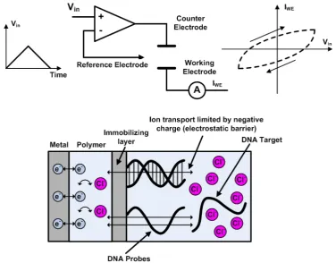
simple detection schemes or even label-free detection by utilizing the electrochemical responses when the biomolecules are under pre-defined electrical excitations. Also, this type of sensor could achieve a very low-cost system implementation by fundamentally eliminating the expensive optical devices for excitation and detection, such as those used by fluorescent detections presented in Section 2.2.1.
In its generic form, this type of electrochemical biosensor is typically composed of one working electrode and one reference electrode with shared or separated ground electrodes. The electrical excitations are either DC signals or low frequency continuous waves (typically in the kHz range). In terms of the fabrication, additional post processing steps may be required to open the passivation layer and form the electrodes with desired metal, such as Au or Pt to facilitate deposition of probe molecules. The detailed sensor circuit design of the electrochemical sensors is determined by the operation technique, which includes impedance spectroscopy (IS), amperometric analysis, redox cycling and cyclic-voltammetry, etc.
In its cyclic voltammetry (CV) operation, the electrical potential on the working electrode is periodically varied with respect to the reference electrode as the excitation signal, while the respective current through the working electrode is measured as the response. This results in specific current-voltage (I–V) curves for different electrical-electrolyte surface. For example, for DNA sensing, since the DNA molecules have overall negative electrical charges due to the phosphate backbone, they will repel chloride ions from the electrode surface. Therefore, if the complementary DNA is hybridized onto the electrode, the increase in the negatively charged phosphate backbone would directly change the kinetics of the chloride ions, and thus alter the shape of the resulting I-V curves. This is shown in Figure 2.5, as follows.
Two types of experiments are performed. One measures the CV response with and without complementary 30-mer target DNAs. At 100nM concentration, the average change for the I–V curve enclosed area is -38%. In the other experiment, the HIV-1 DNA is tested, which results in a 21% area increase. Both results are summarized in Figure 2.6.
Figure 2.6: Measurement results for the CV electrochemical biosensor
2.2.3 CMOS Magnetic Biosensor
The limitation of the above two CMOS biosensor schemes has stimulated research efforts in searching for a new non-optical biosensing modality while maintaining a high sensitivity and a low back-ground noise level. As a result, biosensing based on magnetic micro/nano particle labels have been proposed as one of the promising candidates [16].
Figure 2.7: Magnetic label based biosensing
Current reported integrated magnetic sensor schemes include the Giant Magnetoresistance (GMR) biosensor [6][18][19] and the Hall Effect biosensor [9]. The former, also as a more sensitive sensing scheme, will be discussed here.
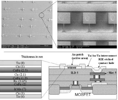
The GMR sensor utilizes the magnetoresistance property whose effective resistance changes when the magnetic labels are drawn close to the sensor surface. An implementation example is given as follows for the GMR sensor [6].
Figure 2.8: SEM photo and the cross-sectional view of the GMR sensor
Figure 2.9: Measured signals for 10nM target DNA and 100nM control DNA with SEM images of particle coverage
2.3 Chapter Summary
In this chapter, we have briefly introduced the biosensor technology. The CMOS process, as a low-cost high-yield implementation tool is demonstrated as a promising platform of biosensor design.
The challenges and opportunities for molecular biosensor are also presented, which requires high sensitivity, good scalability and large parallel processing capabilities. Addressing this advanced sensing application, three CMOS based biosensor schemes, i.e., fluorescence biosensor, electrochemical biosensor and magnetic biosensor are presented with detailed implementation examples.
Chapter 3: Frequency-Shift-Based Magnetic
Particle Sensing Scheme
The chapter is organized as follows. After a background introduction in Section 3.1, Section 3.2 introduces the sensing mechanism of our proposed frequency-shift scheme. Section 3.3 shows the line-width narrowing effect for the LC oscillator’s frequency detection scheme compared with the impedance function sensing scheme based on the same LC tank. This accounts for the ultra-high sensitivity of our proposed scheme. In order to investigate the sensor signal response with the presence of the magnetic particles, the sensor transducer gain is defined and derived in Section 3.4. In addition, the sensor noise floor will be studied and analyzed in Section 3.5. Finally, Section 3.6 presents the sensor signal-to-noise (SNR), which is shown to be entirely determined by the sensing inductor design. Evaluation on the SNR for a wide range of inductor layouts indicates that a smaller sensing inductor gives a better SNR. Design-limiting factors other than the sensor SNR are also presented and discussed in Section 3.6.
3.1. Introduction
Traditionally, microarray technology is used to provide both quantitative and qualitative information for biomolecular sensing [15]. However, to ensure their high sensitivity at the pico-molar level, the microarray system relies on optical detection on attached fluorescent labels, which requires bulky and expensive optical devices including multi-wavelength fluorescent microscopes. This fact fundamentally limits the overall size and cost of the microarray system, which eventually makes the technology unsuitable for PoC applications.
On the other hand, magnetic biosensors are proposed as a promising candidate for these PoC applications. The basic mechanism for magnetic detection and its advantages over fluorescence-based schemes has been discussed in detail in Section 2.2.3. However, in spite of the aforementioned apparent advantages for magnetic sensing, magnetic biosensors developed thus far require externally generated strong magnetic biasing fields and/or exotic post-fabrication processes. This still limits the ultimate form-factor of the system, total power consumption and cost, which unfortunately defeats the original purpose to use the magnetic sensing system for PoC applications [6][8][9][18][19].
3.2. Frequency-Shift-Based Magnetic Sensor Mechanism
The core of our proposed sensing scheme is an on-chip LC resonator. If the test sample contains target molecules, magnetic particles will be immobilized onto the sensor surface after the hybridization procedures shown in Figure 2.7, Section 2.2.3.
Figure 3.1: Proposed frequency-shift-based magnetic particle sensing scheme The current through the onchip inductor generates a magnetic field and thus polarizes the magnetic particles which behave as superparamagnetic materials. This polarization then creates a magnetization for those magnetic particles and increases the total magnetic energy in the space. Consequently, this magnetic energy change leads to an increase of the effective inductance of the resonator, which directly results in a resonating frequency down-shift given by,
1 2 √
1
2 Δ 1
∆
2 3.1
Therefore, by detecting this frequency down-shift, one can infer the existence of the magnetic particles quantitatively. The detailed derivation on how this frequency down shift is related with the presence of the magnetic particles, i.e., the sensor transducer gain, will be derived in Section 3.4.
3.3. Oscillator Based Frequency-Shift Sensing
The mechanism for sensing the presence of magnetic objects by effective inductance change has long been recognized and also widely implemented, e.g., the metal detectors for security check used at airports. However, those traditional implementations are mainly based on sensing the impedance function of the resonator tank directly, which include sensing the change in the amplitude and/or the phase of the impedance function through high-precision circuits, such as a Wheatstone Bridge structure.
However, the impedance function linewidth of an LC resonator, determining the relative amplitude and/or phase shift for a given relative inductance change, is fundamentally limited by the quality factor Q of the resonator. For the on-chip implementation, the quality factor of the resonator is largely dictated by the inductor quality factor, which is very limited, e.g., in the range of 10~20, for a low cost and high substrate conductivity process, such as CMOS. However, the typical relative frequency shift for a single micron-size magnetic particle is in the range of several or sub-ppm (part per million, 10-6). Therefore, this impedance sensing method results in a poor sensitivity, which is not suitable for our magnetic particle detection application.
noise profile compared with the corresponding impedance function line-width, shown in Figure 3.2.
Figure 3.2: Line-width compression effect
This effect is due to the virtual damping phenomena in the active LC oscillators which results in the phase diffusion much slower than the amplitude damping in a normal passive LC resonator by tank dissipation [21]. This line-width narrowing ratio can be estimated as
∆
∆ 1/2
2
· 3.2
where D and are the virtual damping rate and the oscillation frequency for the oscillator and Q is the quality factor for the tank.
Moreover, assuming that the 1/f2 phase noise is dominant, D can be calculated as Δ
2 · Δ 3.3
where Δ is the phase noise power spectrum density at the offset frequency of Δ for the oscillator.
typical values for CMOS implementation. Based on equation 3.2 and 3.3, D ≈ 5.6Hz, and therefore r ≈ 1.8×10⁻⁸.
This significant line-width compression effect suggests that implementing the sensor as an onchip oscillator, whose tank is composed of the sensing inductor and some appropriate capacitors, can result in an ultrasensitive magnetic particle sensor. The narrowed-down phase noise profile thus can easily discern a tiny relative frequency shift, which would be impossible to see with the conventional impedance sensing method with a low Q on-chip LC tank.
The discussion in this section essentially lays the fundamental basis for the high sensitivity performance of our proposed frequency-shift-based magnetic biosensor.
3.4. Sensor Signal Strength
To fully characterize the performance of a sensor system, one needs to model both its signal response and its noise behavior. The sensor signal response with respect to certain amount of sensing targets, i.e., the transducer gain, is derived with an approximate close-form solution in this section, while the sensor noise floor fundamentally limited by the oscillator phase noise will be given in the next section.
With the quasi-static assumption, a current conducting in the sensor inductor, or any equivalent electromagnetic structure, generates a magnetic field at the coordinate
, , according to the Biot-Savart law,
, ,
where the line integration is along the current conducting path and R is the vector pointing from the incremental line vector towards the point , , .
Since most of the commercially available magnetic particles, such as micro/nano magnetic beads, are composed of superparamagnetic nanoparticles dispersed in a nonmagnetic matrix, e.g., polystyrene, its induced magnetization M can be expressed in a Langevin function form (3.5).
· 3.5
where is the total magnetic field inside the magnetic bead, instead of the external excitation magnetic field . Here, we assume the magnetic material is isotropic. At Curie region, with a high temperature or an excitation magnetic field, the Langevin function can be approximated to the classical formula for magnetization which determines the effective susceptibility χ of the superparamagnetic particle as
3 . 3.6
The relative permeability is thus given by
1. 3.7
Since the polarization is an open magnetic circuit problem, demagnetization effect needs to be taken into consideration to calculate the total magnetization given the external excitation field [22]. By applying the demagnetization factor , whose general expression is a 2-dimensional tensor, the magnetic field inside of the bead and the externally applied can be related by
In general, the demagnetization factor depends on the geometry of the magnetic subject under the excitation field. Assuming the magnetic bead is of spherical shape and by taking the average magnetic field inside of the bead, is reduced to a diagonal matrix
of 0 0 0 0 0 0 0 0 0 0 0 0
. Combining equation (3.6) and (3.8) yields the
apparent magnetic susceptibility χ as,
1 . 3.9
Equation 6 demonstrates two important facts. First, χ is always smaller than χ . Moreover, χ has its maximum value of 1/D when χ approaches infinity. This means that even if the magnetic particle is entirely made of ferromagnetic material with high susceptibility (χ is on the order of hundreds or thousands), χ still remains as a small value (1/D which results in a small magnetic signal. This is essentially the fundamental reason why magnetic particle sensing is challenging.
Assume that the volume of the entire space is ; the volume and the apparent susceptibility for the magnetic particle are and ; and the for the ith magnetic particle is ,. Then the total magnetic energy difference for the entire space with or without the presence of the magnetic particles can be calculated as
∆ 1
2 ·
1
2 ·
1
2 , . 3.10
∆ 2∆ 2 ∑ 1
2 , ∑ ,
#
, 3.11
where is defined as the average magnetic flux density for all the magnetic
particles.
Consequently, we can define the transducer gain of our magnetic senor as ∆
# 2 · · . 3.12
This transducer gain equation reveals two important properties of our sensor system. First of all, the sensor sensitivity is proportional to the magnitude square of the averaged excitation magnetic field generated by the sensing inductor. This suggests that the sensor transducer gain has its spatial dependence across the sensor inductor surface. Secondly, the transducer gain is composed of three factors. For a given type of magnetic particle, the first factor determined by the magnetic material property and the last factor of the particle size are both fixed values. However, the factor in the middle is essentially controlled by the sensing inductor, which implies that the sensor inductor design is crucial to achieve a desired transducer gain. These two issues will be discussed in details in the following subsections.
3.4.1 Spatial Variation of the Sensor Transducer Gain
As indicated by equation (3.12), the sensor transducer gain is a function of the excitation magnetic field generated by the sensing inductor, which thereby presents a spatial variation. The transducer gain for a 6-turn inductor with its dout of 140μm, width of 5μm and spacing of 3.5μm for a D=1μm magnetic bead is shown as follows. The passivation layer thickness is 0.9μm. The EM simulation is through Ansoft Maxwell® [24].
gain plateau is thus followed by a gain peak due to both the positive magnetic addition and the close spatial proximity to the inductor traces. Next, the sensor inductor presents a lower transducer gain region due to the addition/cancellation of the magnetic fields from different inductor turns. The transducer gain gradually tapers off outside of the sensor inductor region because of the magnetic field decaying.
For a magnetic particle sensor, a spatially homogeneous transducer gain is preferred. This can be achieved by depositing the probe molecules only onto the plateau region or by confining the microfluidic chamber within that region. Moreover, a homogeneous-gain inductor design can take this spatial gain variation effect into account based on the physical intuitive analysis we just presented.
Figure 3.4: 3D view of the stacked inductor layout
On the other hand, this spatially varying transducer gain also provides extra location information of the present magnetic particles. For example, based on this idea, a “magnetic microscope” may be implemented by a sensing inductor layout with strong spatial gain variations, which detects the attached magnetic particle as well as determining its location.
3.4.2 Sensor Inductor Scaling Rule
As we mentioned in Section 3.4, for the transducer gain expression of equation (3.12), only the middle is within the designer’s control, which is also entirely dependent on the sensing inductor design.
In order to achieve some intuitive design insight for the relationship between the transducer gain and the inductor layout, we can assume isomorphic scaling with a scaling factor on a given inductor geometry. Based on equation (3.12), we can calculate the average transducer gain in the entire effective sensing volume by
· 1 · · 1 · , 3.13
where the effective sensing volume for the given inductor is chosen as the region where the magnetic field magnitude does not decay significantly with respect to the peak magnetic field and the factor represents the product of · , which is independent of the inductor design.
Therefore, the is proportional to . Also, due to the isomorphic scaling, we can approximate the magnetic energy stored in the volume is proportional to the total magnetic energy in space with some proportion constant , as
1
2 ·
1
2 . 3.14
Therefore, the averaged transducer gain across the sensing volume can be further simplified as,
·1 1
2 ·
1
2 1
, 3.15
where is the scaling factor in the isomorphic scaling. The above equation indicates that the smaller the sensing inductor, the larger the average sensor transducer gain. Moreover, the gain is roughly inversely proportional to the 3rd power of the scaling factor.
Figure 3.6: Averaged sensor transducer gain for different inductor sizes (∆L/L per 1μm bead)
3.5 Sensor Noise Floor
The transducer gain introduced in the previous sections models how the sensor will respond to the presence of the sensing targets, i.e., magnetic particles for our study. On the other hand, the sensor’s sensing limit is also determined by the sensor noise floor.
3.5.1 Oscillator Phase Noise
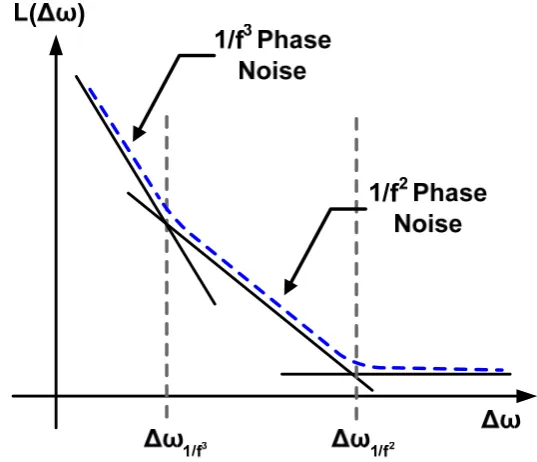
Phase noise represents the frequency instability of the oscillator. In general, a free-running oscillator’s phase noise is composed of two parts. The 1/f3 phase noise at low offset frequencies (typically below kHz range) is mainly due to the up-conversion of the flicker noise power, while the up-conversion of the white noise results in the 1/f2 phase noise [25], shown as follows.
Figure 3.7: Typical oscillator phase noise profile
Generally, the oscillator frequency is determined through frequency counting, which registers the number of transitions of the oscillation waveform within a given time window. Thus the frequency measurement uncertainty is directly determined by the accumulated jitter within this measurement time as
where is the nominal frequency and is the total time for the counting window. Assuming the phase noise experiences a stationary process, the frequency uncertainty can be derived as
∆ 1 · 1 1 · 2 0 . 3.17
By Wiener-Khinchin theorem, the above quantity can be related with the phase noise of the oscillator as
∆
2
0 2 1
4
sin 2 , 3.18
where the is the phase noise profile. These jitter/phase-noise equations will be revisited in Chapter 5 when low noise techniques are introduced.
We can further relate this noise quantity with the inductor design. Assuming a fixed biasing current density for the cross-coupled cores, at the maximum tank amplitude (limited by supply VDD), the biasing current Id, the transistor width W, and the current noise power spectrum density are given by
, , 3.19
At a low offset frequency where the up-converted flicker noise power is dominant, the oscillator phase noise profile can be determined by
·
2 · 3.20
where is the DC term of the oscillator’s impulse sensitivity function (ISF) Γ [26]. This leads to the relation between the sensor noise ∆ and the inductor L and Q as
∆
4
sin 2 . 3.21
This result suggests that the sensor noise floor (due to the oscillator phase noise) also depends on the sensing inductor design.
3.5.2 Temperature and Supply Variations
As we mentioned in Section 3.5, the non-ideal operation environment of the sensor oscillator also leads to non-negligible oscillation frequency shift. Generally, this environmental effect is dominated by variations in the chip temperature and the supply voltage. Since these variations are not known a priori, they can be approximately treated as low-frequency noise/drifting for the oscillation frequency.
Figure 3.8: A generic complimentary cross-coupled LC oscillator schematic with parasitic junction diodes highlighted
The circuit elements which to the first order determine the oscillation frequency are the tank inductor ( , tank capacitor , and the parasitic junction capacitors . The frequency-temperature sensitivity formula can be derived as
1 1
2 1
· 1 · 1 . 3.22
1 1
1
1
, 3.23
where is the doping profile coefficient, is the built-in potential and is the biasing voltage across the junction [27]. Depending on these parameters, a typical temperature coefficient of the junction capacitance is on the range of 250ppm~350ppm/˚C. Based on the relative weight between the tank capacitor and the total junction capacitors, the overall temperature coefficient for the oscillation frequency, shown in equation (3.22) is thus typically smaller than tens of ppm/˚C.
On the other hand, in terms of supply voltage variation, the frequency drift due to the parasitic junction capacitance change will be dominant. This is because the diode biasing voltage is directly related with the supply voltage [27], whose voltage sensitivity can be shown as
1 1
1
1
· 1 . 3.24
3.6 Sensing Inductor Optimization for Maximizing Sensor
Signal-to-Noise Ratio (SNR)
With the analysis results for both the sensor signal strength (transducer gain) and the sensor noise floor, we can therefore arrive at the sensor signal-to-noise ratio (SNR) as
∆
∆ ·
1
· , 3.25
where is the average magnetic flux density across the inductor sensing area. Thus, the sensor SNR is fully determined by the inductor design, which needs to be carefully optimized. Moreover, the inductor layout also limits the basic footprint of a sensor cell. Then choosing the inductor geometry is the key step in designing the frequency-shift based magnetic sensor.
Dout (um)
Width (um)
Relative SNR
1 0.8 0.6 0.4 0.2 0 1 3 5 7 911 275 250 225 200 175 150 125
100
Figure 3.9: Averaged relative SNR for different inductors
As we can see, for a certain Dout, the SNR does not vary significantly with its width. This is because although inductors with a larger width will have a better Q and a smaller L, it has a smaller averaged which leads to an overall relatively constant SNR. On the other hand, for the same turn width, a larger Dout gives a much lower SNR. This is due to the fact that at a larger outer diameter, a smaller averaged together with a larger inductance value result in a significantly degraded SNR.
tank (for a smaller inductor) will conduct a large current, which may result in magnetic saturation for the target particles. This also decreases the actual sensor signal shown in equation 3.12. In addition, for a small size inductor (high peak-Q frequency), a high operating frequency increases its Q, and thus its SNR. But the aforementioned high frequency magnetic loss eventually degrades the magnetic signal and limits the operation frequency to be 1GHz [29] [30]. Besides the SNR consideration, other constrains also limit the design space, including sensor power consumption, hot electron degradation, sensor cell pixel size requirement (foot-print), etc.
3.7 Chapter Summary
In this chapter, we introduce an Effective-Inductance-Change based magnetic particle sensing scheme whose core part is an on-chip LC resonator. Utilizing the phase noise line-width narrowing effect in LC oscillators, we propose a novel sensing method which utilizes the relative frequency shift of the LC resonator based oscillator at the presence of the magnetic particles. This sensing approach can potentially achieve a significantly better sensitivity compared with conventional LC tank impedance sensing method, which is fundamentally limited by the quality factor of the tank.
and the extrinsic (environmental) noise dominated by temperature and supply voltage variations. Further derivation on the oscillator phase noise relates the intrinsic noise floor with the inductor design parameters.
Chapter 4: Frequency-Shift Magnetic
Particle Sensor Implementation
4.1. Introduction
In Chapter 3, we have proposed the frequency-shift based magnetic sensing scheme and studied its mechanism including the sensor SNR and sensor design scaling rule. In this chapter, we will present two sensor implementation examples based for this scheme.
Section 4.2 demonstrates our first version discrete implementation. The sensor circuit is composed of high-frequency low noise bipolar transistors and discrete capacitors. The spiral inductors for desired sensing functionalities are patterned on the thin film circuit board directly. Several experiments are performed, whose measurement results are compared with simulations to validate our modeling analyses shown in Chapter 3. Finally, the limitations of this design implementation are summarized.
sensitivity for CMOS magnetic sensor reported so far. Furthermore, a significant SNR improvement can be achieved by averaging the data samples.
Finally, a summary will conclude this chapter in Section 4.4.
4.2. A Discrete Magnetic Particle Sensor based on Thin-Film
Technology
To verify the proposed sensing scheme, the frequency-shift magnetic sensor is first implemented as a discrete design. The circuit board is based on a one-layer thin-film technology with gold plated traces with a line-width resolution of 20μm [31]. The low loss substrate is made by alumina. These specs are essential to implement a small footprint spiral inductors with a high quality factor. The thin-film board is designed in Protel®and shown as follows.
delivery and subsequent microfluidic channel integration. The inductors specs are shown in the following table.
Table 4.1 SPECS FOR THE FOUR THIN-FILM INDUCTORS
Inductor 1 Inductor 2 Inductor 3 Inductor 4
Outer Diameter (μm) 556 616 676 736
Trace Width/Separation (μm) 20/10 20/10 20/10 20/10
Number of Turns 7 8 9 10
Inductance (nH) 17.2 23.5 31.1 40.2
Quality Factor at (100MHz) 12.4 13.6 14.8 16.0
4.2.1 Sensor Circuit
The sensing oscillator, operating at a nominal frequency of 100MHz, adopts a Coplitts topology for an improved phase noise performance, shown as the following figure with all the main circuit elements denoted.
4.2.2 Measurement Results
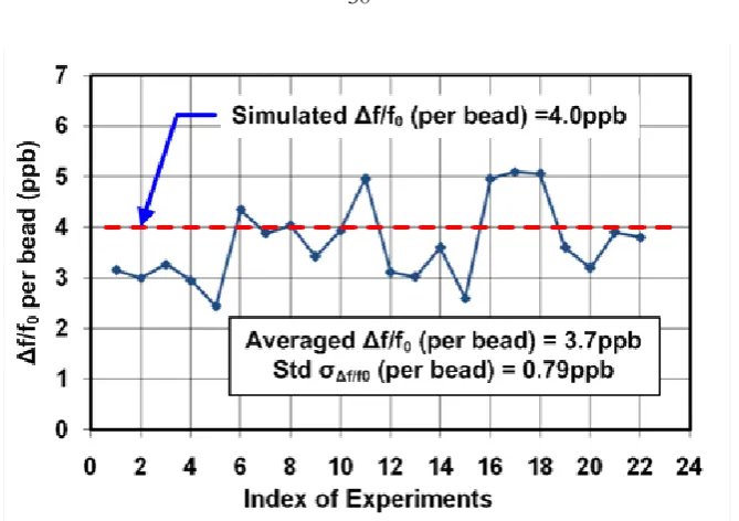
Two measurements are performed for this discrete type magnetic sensor. The first measurement is based on dry experiments which sense the deposited magnetic particles (Dynabeads® MyOne, D=1μm [16]) after the buffer solution evaporates. The second measurement is based on wet experiments, which test the magnetic particle samples in aqueous buffer solutions. In the following part of this section, the two measurements together with their results will be presented.
In the dry experiment, the thin-film sensor oscillator circuit has been coated with parylene (thickness of 3μm). This provides electrical isolation between the deposited magnetic particle samples with the thin-film sensing inductors. Then, magnetic beads solutions with different concentration are deposited on the sensing inductor via pipette (Rainin, D20). Due to the operation of the oscillator, the temperature on the sensing inductor surface increases and leads to a fast evaporation of the water content in the bead samples. A waiting time of 15 minutes is adopted to achieve the thermal steady state. The oscillator’s oscillation frequency is counted by an off-the-shelf frequency counter HP 53150A. The summary on the experiment procedures is listed in Figure 4.3 and the sensing inductor (Inductor 2) with deposited magnetic particles is shown in Figure 4.4.
Figure 4.4: Sensing inductors deposited with target magnetic particles
Typical measurement results of frequency counting with respect to time are shown in Figure 4.5. For this frequency plot, the total number of magnetic beads is around 45000. Traces with different colors represent different measurements. Before applying the magnetic beads, the oscillator frequency is measured as the baseline frequency. After applying the magnetic beads, the frequency is again recorded. The difference in frequency indicates the detected signal due to the magnetic particles. The experiment is then repeated and a result summary is shown in Figure 4.6.
Figure 4.6: Measurement results summary on the dry experiment
The averaged ∆f/f0 per bead from the measurement results is 3.7ppb, which is in close agreement with the averaged ∆f/f0 per bead of 4.0ppb based on electromagnetic simulation. Although the error bar of 0.79ppb is not small, mostly due to the inaccuracy of sample delivery and oscillation frequency jittering due to thermal variation, the experiment still verifies that our sensor scheme is practically valid with the dry magnetic particle samples.
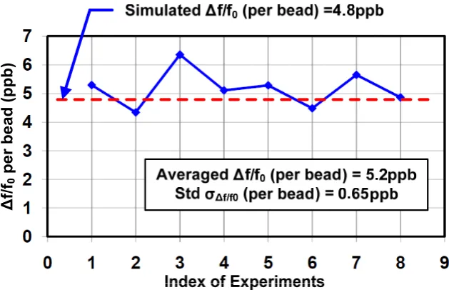
module together with the PDMS microfluidic device is shown in Figure 4.8. The measurement procedure is shown in Figure 4.9.
Figure 4.7: PDMS microfluidic structure
Figure 4.8: Sensor module with the PDMS microfluidic device
Figure 4.10: The delivered magnetic beads on the sensor inductor (Inductor 1) A picture of magnetic beads delivered on the sensor inductor (Inductor 1) is shown in Figure 4.10. A summary on the measurement result is shown in Figure 4.11. As we can see the average ∆f/f0 per bead from the measurement results is 5.2ppb while the ∆f/f0 per bead by simulation is 4.8ppb. The increase on the average frequency shift per bead is due to the fact that the delivered magnetic particles tend to aggregate to the positions where a large magnetic field is present, shown in Figure 4.10. Overall, this aqueous experiment still shows that our sensor scheme is practically viable with the magnetic particle carried by aqueous buffer solutions.
Δ
f/f0
per bead (ppb)
In summary, this discrete implementation of our proposed sensor scheme verifies that by using the relative frequency shift (inductance change) of the LC resonant tank, micron-size magnetic particles are indeed detectable.
4.2.3 Limitation and Potential Improvement
As presented in the previous sections, the discrete design verifies the functionality of our frequency-shift based magnetic sensor scheme. However, there are following limitations on this particular implementation.
First of all, the sensor transducer gain is low. As we have shown in the measurements, for Dynabeads® MyOne (D=1μm), the signal strength is typically 3~5ppb/bead. This is not a surprising result, since low sensitivity for large inductor footprint is predicted by our analysis in Chapter 3. However, due to the fact that the inductor trace width is limited by the thin-film process and the parasitic inductance for connecting the tank is prominent in the discrete design, inductors with large peripherals (large inductance) are still used for this implementation. Based on our studies in Chapter 3, the way to significantly increase the signal strength is by decreasing the size of the sensing inductor and therefore operating at a higher oscillation frequency. This is practically suitable for an integrated implementation.
two oscillators essentially suppresses the low-frequency drift due to all these environmental factors. This differential sensor scheme also prefers an integrated implementation, where matching within the sensor pair can be reliably achieved.
Furthermore, the temperature of this sensing oscillator may vary during the sensing operation, particularly when samples are delivered onto the sensor surface. This leads to significant frequency drift due to the non-zero temperature coefficient of the oscillator discussed in Chapter 3. In order to register the oscillation frequency at the thermal steady-state for a fair comparison between the target samples and the control samples, a long waiting time is unavoidable. Therefore, to facilitate fast data acquisition, a temperature controller implementation is required to actively stabilize the temperature of the sensor.
4.3. A Fully Integrated CMOS Sensor Array with PDMS
Microfluidics Sample Delivery
Based on the measurement results and further discussions on our discrete sensor implementation in Section 4.2, we find that our sensor performance can be substantially improved if we implement the scheme in integrated form.
onto the CMOS chip will be presented. The measurement of the integrated sensor implementation will eventually conclude this section.
4.3.1 Sensor Array System Architecture
To fully explore the strength of scaling and parallel processing in CMOS technology, we have implemented the sensor structure in an 8-cell array [35]. This potentially enables the sensor system to detect eight different types of bio-samples simultaneously. The sensor architecture is shown in Figure 4.12.
Figure 4.12: The 8-cell CMOS sensor array system architecture
operating at a 1GHz nominal frequency. In the layout, the two oscillators are placed in close proximity to each other to improve matching and minimize their on-chip temperature difference. The oscillator pair also shares the power supply, biasing and ground line, which ensures that the differential operation will suppress the low-frequency common-mode noise and drifting described in Section 4.2.3. The detail design issues for sensing oscillator will be presented in Section 4.3.2. Also, based on Section 4.2.3, to improve the sensor sensitivity, in terms of the design, a smaller foot-print sensing inductor should be used, which leads to a higher operating frequency. However, the upper limit of the operating frequency is determined by the magnetic material under test. For micron-size magnetic beads composed of nano-magnetic particles dispersed in a nonmagnetic polystyrene matrix, they typically experience a significant magnetic loss for a frequency above 1GHz in that the real part of their permeability starts to decrease while the imaginary part increases dramatically. This is essentially non-ideal for our magnetic sensing. Therefore, we choose 1GHz as our sensor operating frequency.
A temperature controller is implemented locally for every sensor cell. It regulates the on-chip temperature for the oscillator active cores through a thermal-electrical feedback loop to minimize the frequency drifting effect induced by the ambient temperature change. The details for temperature regulator design will be presented in Section 4.3.3.
down-conversion architecture is used to shift the frequency center tone of 1GHz to a baseband frequency below 10kHz. Unlike direct downconversion, this architecture guarantees that neither of the LO signals are close to the sensor free-running frequency nor its harmonics and hence prevents oscillator pulling or injection locking on the sensing oscillator pairs. By using a baseband 15-bit frequency counter, a frequency counting resolution of better than 0.3Hz (3×10⁻⁴ppm) is thus achieved.
4.3.2 Sensor Core Design
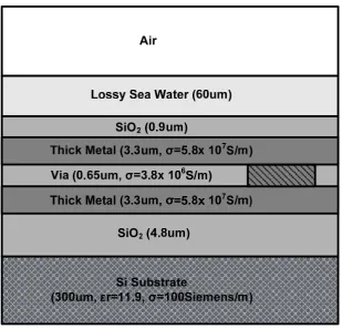
As we have mentioned in Chapter 3, the first step for designing the frequency-shift magnetic sensor is to determine the inductor design. Based on the electromagnetic simulation on a TSMC 130nm CMOS process with a dual thick copper (3.3μm thickness) option, the sensing inductor design is chosen as a 6-turn symmetric inductor, with the dout of 140μm, width of 5μm and trace separation of 3.5μm. Note that in real biology experiments, this sensor oscillator may need to operate with samples under aqueous condition. The water content may introduce extra loss to the inductor. Therefore, to have a conservative estimation on this Q degradation, we have added an extra layer of sea water, 60μm in height, on top of the SiN passivation layer with its bulk conductivity of 4siemens/m and a frequency-dependent dielectric loss tangent table to capture both the ionic loss and the dielectric loss across the simulated frequency.
Inductance=3.1nH Q=10.6
Frequency (GHz)
Differential Inductance (
n
H)
Differential Q
Figure 4.13: The effective differential inductance and its quality factor
Figure 4.13 shows that even with the lossy sea-water layer, the inductor still achieves its Q of 10.6 at the 1GHz operating frequency, which is suitable for a high-quality low-noise integrated oscillator implementation.
Based on this inductor layout, the average sensor response to a single one D=1μm magnetic bead is around 0.45ppm/bead by numerical simulations on our close-form formula in Chapter 3.
A sensor oscillator can be designed by using this inductor geometry. We have adopted a differential complementary cross-coupled oscillator biased with an NMOS current source. The relative weight between the NMOS active pair and the PMOS active pair has been carefully optimized to minimize the flicker noise up-conversion from the NMOS current tail. Moreover, to improve the matching, a novel layout for a fully symmetric cross-coupled pair is adopted, which improves the intrinsic oscillator frequency stability and the robustness against process gradient.