Static Noise Margin Analysis during Read
Operation of 7T SRAM Cells in 45nm
Technology for Increase Cell Stability
Shelendra Singh Tomar
M.Tech VLSI
Institute of Technology and Management, Gwalior, India [email protected]
Madhav Singh
M.Tech VLSI
Institute of Technology and Management, Gwalior, India [email protected]
Shyam Akashe
Assistant Professor
Institute of Technology and Management, Gwalior, India [email protected]
Abstract:
In this paper we introduce Noise (the Static Noise present in 7T SRAM cell) effect the stability of cell. Actually SNM is present in SRAM cell which is effect the stability in read operation of the 7T SRAM cells. SRAM cell stability analysis is a based on Static Noise Margin (SNM) investigation when in read mode, although many memory errors may occur during read operations. So that SNM varies with each cell operation, a thorough analysis of SNM in read mode is required. In this paper we investigate the SRAM cell SNM during read operations analyzing various alternatives to improve cell stability in this mode. The techniques studied are based on transistor width, and word- and bit-line voltage modulations. We show that it is possible to improve cell stability during read operations while reducing word line voltage.
Index Terms— Cell Ratio, CMOS, Data Stability, Pull-up Ratio, Static Noise Margin (SNM), VLSI.
1. Introduction
2. The 7T SRAM Cell Stability
The 7T SRAM Cell stability is depend on SNM and SNM is depend on PMOS and NMOS transistor width. The circuit of 7T SRAM cell is made of two CMOS inverters that connected to cross coupled to each other with additional NMOS Transistor which connected to read line and having two pass NMOS transistors connected to bit lines and bit-lines bar respectively. Fig 1 shows circuit of 7T SRAM Cell, where the access transistors MN3 is connected to the word-line (WL) to perform the access write and MN4 is connected to the Read-line (R) to perform the read operations thought the column bit-lines (BL and BLB). Bit-lines act as I/O nodes carrying the data from SRAM cells to a sense amplifier during read operation, or from write in the memory cells during write operations. All transistors have minimum length (Lmin =45nm according to used Technology), while their widths are typically design parameters. The value of Wp1 and Wp2 defines PMOS transistors width and Wn1 and Wn2 defines the NMOS driver transistors width use in CMOS Invertors, while Wn3 and Wn4 is the access transistors width.
Figure 1. 7T SRAM cell schematic.
2. Static Noise Margin
Butterfly curve method is used for measuring static noise margin. Static Noise Margin of the SRAM cell depends on the cell ratio (CR), supply voltage and also pull up ratio. For stability of the SRAM cell, good SNM is required that is depends on the value of the cell ratio, pull up ratio and also for supply voltage. Cell ratio is the ratio between sizes of the driver transistor to the load transistor during the read operation. Pull up ratio is also nothing but a ratio between sizes of the load transistor to the access transistor during write operation [1]. The basic circuit of SRAM cell is shown in given below as figure 1.
(During Read Operation)
(During Write Operation)
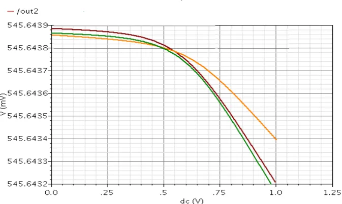
two-Figure 2. "Butterfly" curve measuring SNM.
Fig. 2 shows the "butterfly" curves for 45nm technology for 1.0 v supply voltages. The Figure shows that the static noise margin (SNM). SNM is a taking important factor during read mode, during read operation values varies in different operation mode. It has been shown that during read the SNM takes its lowest value and the cell is in it operate state. During read operation taking SNM when the word line is set high and both bit-lines are still pre-charged high. While in this situation, the SRAM cell internal node being low will be pulled up through the access transistor degrading significantly the SNM during the read operation during read operation that illustrate the degradation in SNM during read and how lowering the supply voltage further aggravates the impact on SNM Table 1 lists the SNM values during read operations at two different power supply voltages corresponding to a minimum sized bit-cell.
Table 1. SNM Read Vs Vdd
SNM(mV) VDD=1.0V VDD=0.8V
READ 240.95mV 229.88mV
3. SNM dependences
We can analyses with the Table 1 and Fig 2 that the value of SNM is changes in Read operation. We have taken different parameter on SNM while taking read mode.
3.1. Word-line modulation
Figure 3. SNM Vs Word-line voltage.
SRAM cell access can be controlled with the help of word-line voltage it is very useful during Read operation. According to the Fig 3. when the word line voltage decreases the SNM is increases respectively during read operation. We have seen that while reducing word line voltage the stability of 7T SRAM cell is increased during read operation We have taken the value of α and β in worst case as shown in table 2. The SNM can be improved by with the help of width transistor and word-line voltage modulations, The values of α and β ratios for these three cases are sum.
Table 2. Different parameters
Worst Case Minimum
Distance
High SNM
α 1 1 2.5
β 2.5 1 1
The result of combining both width and voltage modulations highlights two main points: first, SNM improvement is maintained and increased and second, a different behavior during hold and read modes is obtained. While the high-SNM curve is lower than the others in hold mode, during read mode the High-SNM curve is the top one. This indicates that the cell stability may not be well defined by SNM given its dependence on the cell mode.
3.2. Bit-line modulation
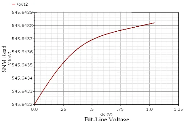
Bit line voltage is effectively changes the value of SNM in this operation we evaluate precharged bitline at full power supply voltage. Fig. 5 Shows the graph between the SNM and the bit-line voltage. In this graph the SNM can be increases by reducing below Vdd the bit-line voltage during read operations. This technique increases the cell stability and is suitable for voltage modulation.
Figure 5. SNM Vs Bit-line voltage modulation
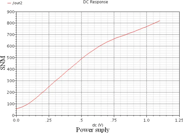
3.3. Power-Supply voltage modulation
Figure 6. Impact of Power Supply voltage modulation on SNM.
However, it is possible to maintain are reduced Vdd during read operation and compensate for the SNM reduction through the voltage modulation techniques described earlier. The wordline voltage modulation may provide a better read mode SNM at (2/3)Vdd by lowering the word-line voltage to about 0.6v of the nominal value. Table 3 provides numerical values of the read-mode SNM for some combination of word- and bit-line voltage modulation voltages (modulated SNM) together with transistor width modulation[2]
Table 3. SNM READ Vs Vdd.
Vdd SNM read WL BL α β SNM READ
(MODULATED)
1.0 158.12mV 0.9 0.9 1 1 240.95mV
0.9 146.57mV 0.9 0.9 1 2 236.37mV
0.8 131.88mV 0.9 0.9 2 2 229.88mV
4. Simulation and Result
We have seen that during a read operation, the Static Noise Margin analysis indicates that the stability of the cell is degraded. In this paper we show that how bit line and word line voltage effect the SRAM cell stability because these are the important parameters in SRAM cell operations. The supply voltage also play vital role in SRAM cell stability during read mode of SRAM cell also by lower power supply may reduce the leakage current for all cells in the memory. The world-line voltage, the bit-line voltage and the power-supply voltage all three voltages could be used to improve the SNM.
SNM calculation: We have done the SNM calculation by this way with respect of above figure butterfly curve: Side of the Maximum Square =A=0.240V=240 mV,
Lengths of diagonal of Square (D) = √ 2 * One side of the Square =√ 2 * 240 SNM= D/ √ 2 =√ 2 * 240/√ 2
So, SNM =One of the side=A=240 mV.
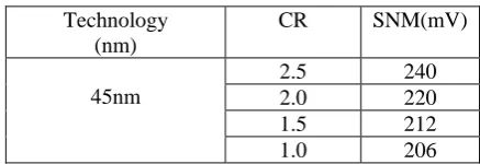
Table 4 SNM Vs CR on 45nm Technology
Technology (nm)
CR SNM(mV)
45nm
2.5 240 2.0 220 1.5 212 1.0 206
The range of the cell ratio and pull-up ratio lie in 1.0 to 2.5 and 3 to 4 respectively otherwise data will be destroy. We have taken some cell ratio vs. static noise margin in Table 5, the value of static noise margin increases with the increase of the cell ratio of the SRAM cell in 45nm technology. If the value of the driver transistor is increased then CR is increased. Result the SNM and speed is also increased.
5. Acknowledgement:
I am very thankfully to ITM University for providing a good lab facility. We simulate the Result on CADENCE VIRTUOSO Tool.
7. References
[1] Andrei Pavlov & Manoj Sachdev, “CMOS SRAM Circuit Design and Parametric Test in Nano-Scaled Technologies”. Intel Corporation, University of Waterloo, 2008 Springer Science and Business Media B.V., pp:1 202.
[2] B. Alorda, G. Torrens, S. Bota and J. Segura Univ. de les Illes Balears,” Static-Noise Margin Analysis during Read Operation of 6T SRAM Cells” Dept. Fisica, Cra. Valldemossa, km. 7.5, 07071 Palma de Mallorca, Spain
[3] Debasis Mukherjee, Hemanta Kr. Mondal and B.V.R. Reddy,” Static Noise Margin Analysis of SRAM Cell for High Speed Application” IJCSI International Journal of Computer Science Issues, Vol. 7, Issue 5, September 2010
[4] Benton H. Calhoun, Member, IEEE, and Anantha P. Chandrakasan, Fellow,” Static Noise Margin Variation for Sub-thresholdSRAM in 65-nm CMOS” IEEE, IEEE JOURNAL OF SOLID-STATE CIRCUITS, VOL. 41, NO. 7, JULY 2006
[5] AMINUL ISLAM AND MOHD. HASSAN “VARIABILITY ANALYSIS OF 6T AND 7T SRAM CELL IN SUB-45NM TECHNOLOGY” IIUM Engineering Journal, Vol. 12, No. 1, 2011