An Area Efficient 3T XNOR cell based Low
Power Full adder using 32nm Technology
Ramesh Jangir1, 2, a), Ramakant Vyas3
1. Department of ECE, B.K.Birla Institute of Engineering and Technology, Pilani, 333031. 2. M. Tech Scholar, Department of ECE, Shekhawati Engg. College,Dundlod, Jhunjhunu
3. Assistant Professor, Department of ECE, Shekhawati Engg. College,Jhunjhunu
Abstract: Full adder cells are the bricks of arithmetic & logical modules and these modules are bricks of the microprocessors and DSP. In the current age of technology advancement it is necessary to design different new concepts to reduce area of the cell as well as power consumption. In this paper CMOS gates have been used to develop the proposed XNOR bricks using 3 transistors and mux using 2 transistors. These bricks are designed to reduce the power consumption and the chip area occupied by it. The proposed design of full adder uses 8 CMOS transistors (3 PMOS + 5 NMOS). The reduction in CMOS transistors improves area and power performance. The proposed full adder cell have been designed using 32 nm CMOS technologies. The developed full adder cell with 3T XNOR bricks with have shown an improvement of 47% in power and 23.92% in area using DSCH3.5, Microwind 3.1tool at 32nm CMOS technology so as to implement adder cell efficiently for DSP applications.
Index Terms---DSCH, full adder, transmission gate (TG), Mux, and XNOR
I. INTRODUCTION
The modern technological advancement & research area are heavily emphasized on exponential growth of multimedia as well as communication devices like mobile phones, laptops and smart devices for everyday life. This development demands that digital circuitry keep up with the phase [1]. CMOS Addition is the fundamental arithmetic operation done in system at the elementary level. Full adders are used for the purpose of addition in many VLSI circuit such as application specific DSP architectures, microprocessors, etc. So the performance parameters of the circuit that includes power consumption, chip area, delay depends upon the design of the full adder [2]. Full adder is very important as it is the base of every ALU operation like subtraction, multiplication,
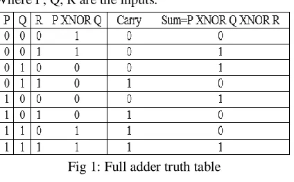
division, etc. and it also gives the feature of carry propagation. The effect of the choice of the design of the full adder is very significant. The power consumption of the full adder depends upon the switching activity and the size of the transistors. The area depends upon the number and size of the transistors. Time delay depends upon the number of transistors and the parasitic capacitance. Some mechanism like cooling and packaging become more complex and costly with huge power consumption [3]. Low power is one of the most important criteria for integrated circuit designers at each levels of chip design along with other parameters like area and power delay. Power consumption in VLSI circuits are focused on switching power, short circuit power and static power [4]. In this paper we proposed a full adder optimized circuit in terms of area, power and delay. The proposed circuits consists of XNOR cells like previous literature of adder circuit based on XOR/XNOR cells [5, 6]. The Full adder is a combinational circuit with three inputs, Bit1 (P), Bit2 (Q), Bit3 (R) and two outputs sum and carry. The boolean expression for Sum and Carry is given below [7]:
RP QR PQ Carry
R Q P Sum
(1)
Where P, Q, R are the inputs.
Fig 1: Full adder truth table
XNOR gates and mux consumed considerable chip area for their optimized performance rather than the circuit designed in paper [9].
II. PREVIOUS WORKS
Various full adder circuits have been introduced in literature [7] - [9] with CMOS level implementation. 26 transistors conventional full adder is presented at beginning stage of evolution later the transistor count keep on decreasing mode as technology moves towards advancement in terms of area [10].
Fig 2: 26T conventional full adder [10]
In the literature full adder design contains equal no. of PMOS and NMOS transistors [12]. Due to large count of transistor cells, its power consumption is large. More no. of PMOS transistor in pull up network results in large value capacitances, which cause high delay and dynamic power. One of the most significant advantages of this proposed full adder is in terms of less area, power and delay.
Fig 3: Structure of single bit Full Adder [10]
This block diagram shows that an adder cell is divided into three parts to produce outputs. Module 1 and module 2 represents the same cell like
XOR/XNOR and module 3 represents 2:1 multiplexer. Ten transistor XNOR based full adder shown in fig. 4.
Fig 4: 10 TG XNOR Full Adder [10]
This paper reveals and compare different full adder structures in terms of area and power consumption as well as power delay product (PDP). Paper shows that an adder circuit is implemented using 2 XNOR cell and one 2:1 mux.
III. PROPOSED WORK OVERVIEW
In the proposed design, full adder circuit is realized by using module 1 & module 2 as 2 XNOR gates and module 3 as 2:1 MUX. The proposed XNOR cell is designed using inverter and one NMOS transistor as shown in fig. 5 are used to get the Sum when output of this cell is again processed with another similar module and MUX is used to get carry.
XNOR WORKING
In the proposed XNOR cell 1 PMOS transistor and 2 NMOS transistors are used. The system’s behavior for different inputs is described:
Case 1: For input, P=0 & Q=0, PMOS1 will be on and NMOS1 & NMOS2 will be off, so the output will be high as the Vdd is directly going to the output
due to on state of PMOS1 and it is not discharged to the ground because no conducting path is present due to off state of NMOS1 & NMOS2.
Case 2: For P=0 & Q=1, NMOS2 will be off & PMOS1 and NMOS1 will be on, due to which the output node will be high as well as low for respective transistors. There is no conducting path from output node to ground. There will be a threshold drop in the NMOS1 and to maintain the high output swing and reduce the threshold voltage drop and to reduce time delay, channel width of PMO1 can be decreased.
Case 3: For P=1 & Q=0, PMOS1 & NMOS1 will be off and NMOS2 will be on due to high logic at the gate terminal of NMOS2. So there will be a conducting path present from Output node to ground which discharges it.
Case 4: For P=1 & Q=1, NMOS1 & NMOS2 all will be on. So the output node will be discharged to the ground. PMOS1 will be off and NMOS1 will be on due to their respective inputs.
There are two XNOR gates which are cascaded to generate the SUM.
MUX WORKING
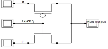
The truth table of carry is produced by 2:1 mux as inputs (R, P) & select line as P XNOR Q. When P XNOR Q=0, carry table fill with values similar to R and P XNOR Q=1, values similar to P.
Fig 6: 2:1 multiplexer for carry implementation
Proposed Full Adder:
As per fig. 1 (P, Q and R) are input to the full adder and sum & carry are the outputs. The proposed full adder sum is Sum= (P XNOR Q XNOR R) but functioning of carry output is quite different and mentioned in fig. 6. So this proposed phenomena reduces the chip area and power consumption because of only two transistors are used. XNOR gate is designed using 3T and MUX is designed using 2T. So total number of transistors is 3T+3T+2T = 8T shown in fig 7.
Fig 7: 8T XNOR based proposed full adder
IV. RESULT SIMULATION & ANALYSIS
Reduction of power consumption reveals a great improvement to a full adder circuit. Power consumption lead to over consumption when devices are serially added in larger circuit. This power reduction would come at the expense of overall speed and increased delay.
Proposed full adder cell is designed by using 8 transistors is shown in fig. 7. This full adder cell is designed by using 3 transistor XNOR circuit shown in
fig. 5 and 2 transistor mux circuit shown in fig 6. Area and power consumed by this proposed circuit is less as compared to full adder circuit made by XNOR circuit in fig 4.
Fig 9: Layout of proposed 8T XNOR full adder cell
Schematic of eight transistor XNOR based full adder cell is designed using DSCH3.5 tool. Simulation has been done by verifying truth table in fig. 1. Layout of the 10T, proposed (8T) XNOR based full adder has been implemented using microwind version 3.1 shown in fig. 8 & fig. 9 respectively.
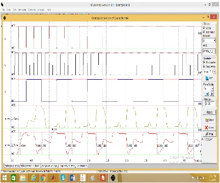
These layout fig. also shows the area of the circuit & for power consumption analog simulation has been done through the same tool at 32nm CMOS technology shown in fig. 10 & fig. 11. Both fig. shows how proposed 8T XNOR based full adder design is consuming less power than 10T XNOR based full adder design.
Fig 10: Analog simulation result of 10TG XNOR full adder cell
Fig 11: Analog simulation result of proposed full adder cell
On the basis of MICROWIND 3.1 designing tool the performance comparison in table 1 between area and power of full adder cell by 18T, full adder cell design using 2: l MUX which consist 14 transistors and 10TG XOR/XNOR based full adder & 8T XNOR proposed full adder cell. Different full adder cell comparison is shown in table1 below. Power consumed by each cell is 3.68uw, 3.68uw, 1.534uw, 0.842uw, 0.813uw respectively. Power consumed by proposed 8T XNOR full adder is least. Area of the proposed adder cell is also least among literature cells.
Table 1: COMPARATIVE STUDY OF AREA AND POWER OF VARIOUS FULL ADDER DESIGNS
Design Power Area Transistor count
18TG FA 3.68uw 58.4um2 18
14TG FA 3.68uw 41.2um2 14
10TG XNORFA
1.534uw 25.5um2 10
10TG XORFA
0.842uw 25.5um2 10
8T FA (Proposed)
0.813uw 19.4um2 8
V. CONCLUSION
power consumption. So in this paper transistor count is reduced as much as possible. The design shows comparatively optimized area & power as compared to the state of art. Area of the proposed full adder cell is reduced from 25.5um2 to 19.4um2. Power consumption of the proposed adder cell is reduced from 1.534uw to 0.813uw. The main focus of the future work is to reduce the more power consumption, area and delay while meeting the required design constraints.
ACKNOWLEDGEMENT
Author would like to thank Dr. P.S. Bhatnagar, Director B.K.B.I.E.T, Dr. L. Solanki, Principal B.K.B.I.E.T, without their support and valuable guidance things would not have been practically implemented. Last we would thank our colleagues Mr. Shashi Kant Sharma, Mr. Buddhi Prakash Sharma & Mr. Sanjay Kumar Saini for giving their endless support.
REFERENCES
[1] J. M. Wang, S. C. Fang, and W. S. Feng, “New efficient designs for XOR and XNOR functions on the transistor level,” IEEE J. Solid-State Circuits, vol. 29, no. 7, pp. 780–786, Jul. 1994. [2] Y. Leblebici and S.M. Kang, CMOS Digital Digital Integrated Circuits, Singapore: Mc Graw Hill, India, 2nd edition, 1999. [3] H. T. Bui, A. K. Al Sheraidah, and Y.Wang, “New 4-transistor XOR and XNOR designs,” in Proc. 2nd IEEE Asia Pacific Conf. ASIC, 2000, pp. 25–28.
[4] H. T. Bui, Y. Wang, and Y. Jiang, “Design and analysis of low-power 10-transistor full adders using XOR-XNOR gates,” IEEE Trans. Circuits Syst. II, Analog Digit. Signal Process, vol. 49, no. 1, pp. 25– 30, Jan. 2002.
[5] S. Goel, M. E. Elgamel, M. A. Bayouni, and Y. Hanafy, “Design methodologies for high- performance noise-tolerant XOR-XNOR circuits,” IEEE Trans. Circuits and Syst. I, vol. 53, no. 4, Apr. 2006.
[6] Shiv Shankar Mishra et.al. “New design methodologies for high speed low power XOR-XNOR circuits,” World Academy of Science, Engineering and Technology, vol.55, pp.200-206, 2009. [7] Sohan Purohit and Martin Margala, “Investigating the Impact of Logic and Circuit Implementation on Full Adder Performance” IEEE Transaction Very Large Scale Integration (VLSI) Systems, Vol. 20, no.7, pp.1327-1331, July 2012
[8] Anjali Sharma, Richa Singh and Rajesh Mehra, “Low Power TG Full Adder Design Using CMOS Nano Technology”, 2nd IEEE International Conference on Parallel, Distributed and Grid Computing, pp. 210-213, 2012
[9] Buddhi Prakash Sharma and Rajesh Mehra, “High Speed & Power Efficient Inverter using 90nm MTCMOS Technique,” International Journal of Scientific Research Engineering & Technology, pp. 21-25, August 2014.
[10] Shivani Singh, Buddhi Prakash Sharma, Sanjay Singhal, “An Area Efficient Low Power TG Full Adder Design using CMOS Nano Technology”, International Journal of Engineering Research & Technology (IJERT), ISSN: 2278-0181, Vol. 3 Issue 4, April – 2014, pp. 2197-2201.
[11] Partha Bhattacharyya, BijoyKundu,SovanGhosh, Vinay Kumar and AnupDandapat, “Performance Analysis of a Low-Power High-Speed Hybrid 1-bit Full Adder Circuit”, IEEE Trans. Very Large Scale Intsgr. (VLSI) Syst., vol. 23, no. 10, October 2015.
[12] D.lakshmaiah, T.sai baba et. Al, “Design of Low Power CMOS Three Input XOR/XNOR”, International Journal of computer science and Electronics Engineering UK, Vol. 6, Issue 1, pp. 1-6, May 2016.
![Fig 4: 10 TG XNOR Full Adder [10]](https://thumb-us.123doks.com/thumbv2/123dok_us/8585830.1719872/2.612.73.284.521.641/fig-tg-xnor-full-adder.webp)