ISSN: 2231-5381
http://www.ijettjournal.org
Page 4540
Design And Implementation Of Multiple Output
Switch Mode Power Supply
Amit1, Dr. Manoj Kumar2
1
Student of final year B.Tech. E.C.E., Guru Jambheshwar University Of Science & Technology, Hisar
2
Assistant Professor, E.C.E. Dept., Guru Jambheshwar University Of Science & Technology, Hisar – Haryana-India 1
Abstract— In this paper, the design of multiple output power
supply is presented. An Embedded system requires different voltage levels for its proper functioning because the components used in any embedded system required different voltage levels as per their specifications, so this paper proposed a power supply that includes +15V, -15V, +5V, -5V, +3.3V, +5V Isolated voltage levels. The input for this power supply is 48V DC which is available at all telecom sites. This power supply is capable of providing approximate 40W output power with 80% efficiency. The power supply design topology selected for this paper is flyback converter because flyback converter is a better option as compare to other topologies for low power design and for generating multiple output voltage levels. This power supply is designed by low cost and highly efficient discrete components and the paper also describes the criteria of choosing these components. This supply designed here can be used for almost all applications in telecom embedded products due to its versatile range of constant output voltage levels.
Keywords— Switch Mode Power Supplies, flyback converters, DC-DC converters
I. INTRODUCTION
Modern embedded electronic systems require high quality, small, lightweight, reliable, and efficient power supplies [1]. SMPS are widely used in Telecommunication applications [2]. The main applications of these SMPS are to provide supply to the various control parts, sensors, actuators/relay drives and of course to the different electronic IC’s with high power density, high efficiency and constant operational frequency. SMPS topologies can be classified according to the method of power transfer from the input to output and are classified in flyback and forward groups. In the forward group, power is transferred to the output when the main switch conducts i.e. during ON state, whereas in the flyback group, the power is transferred to the output when the main switch opens i.e. during OFF state [3]. The flyback SMPS topology has been attractive for a long time because of its simplicity when compared with other topologies used in low power applications [4].
II. TOPOLOGY OVERVIEW
The flyback SMPS topology is based on Flyback DC-DC Converters. DC-DC Converters can be classified as isolated and non-isolated. Flyback converter is one of the simple topology in isolated converters [5]. Fig.1 shows the typical topology of flyback DC-DC converters.
Fig. 1 Simplified flyback converter
The input dc source VDC and switch Q is connected in
series with the primary transformer. The diode D and the RC output circuit are connected in series with the secondary of the flyback transformer. The Dot-ends of inductors determines the operation of the DC-DC converter. Polarity of primary winding (Lp) and secondary (Ls) are not same. When the
switch Q is on, the current in the magnetizing inductance increases linearly and the primary current Ip raises to peak
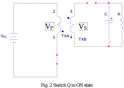
value [6]. At this interval, secondary winding is oppositely polarized to the primary inductor as a result diode D is off and there is no current in the ideal transformer windings. This is shown below in fig 2.
Fig. 2 Switch Q in ON state
When switch Q is turned-off, stored energy at the air gap and magnetic core are transferred to secondary winding and magnetizing inductance current is supplied to the RC load. This is shown below in fig 3.
VDC 1 TXA
2
TXB
3
4
Q 2
1
3
D
+
C R
VDC 1 TXA
2
TXB
3
4
+
C R
ISSN: 2231-5381
http://www.ijettjournal.org
Page 4541
Fig. 3 Switch Q in OFF state
The dc voltage transfer function defined as the ratio of the output voltage to the input voltage of the flyback converter is
= =
(1− )
D is duty ratio of the switch defined as a ratio of the ON time of the switch to the sum of the ON and the OFF times. For a constant frequency operation,
=
is the winding turns ratio given by =
Where and are the primary and secondary winding turns.
Flyback Converter can easily operate in two modes, Continuous Conduction Mode (CCM), Discontinuous Conduction Mode (DCM) [5]. As shown in figure 4, during the Q on time, there is a fixed voltage across the primary winding so primary current will ramps up linearly. As secondary diode is reverse biased so there is no secondary current during . Primary current is maximum at the end of period. When Q turns-off, the magnetizing current in the primary winding stops and the voltage of secondary winding will reverse, to create the flyback action. Due to this reverse secondary voltage diode start conducting and a decreasing secondary current flows in the secondary winding as shown in figure. During this off period, primary winding is not conducting and so primary current does not exist.
In Discontinuous mode, the output winding current goes to zero before the end of the period, so that all the stored energy is transferred to the load.
In Continuous mode, the secondary current is greater than zero when Q turns-on for the next period hence Secondary current couldn’t fully discharge at any time, so there is some residual energy stored in the transformer at the end of the every ON and OFF periods.
Fig.4 Flyback converter waveform: Discontinuous Mode vs. Continuous Mode
(a) Q Command Voltage (b) Primary Voltage (c) Primary Current (d) Secondary Voltage (e) Secondary Current.
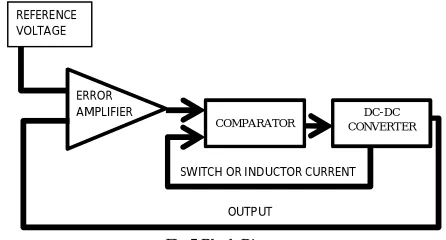
III. BLOCK DIAGRAM OF THE SYSTEM
The dc–dc converter provides a regulated dc output voltage under varying load and input voltage conditions. The converter component values are also changing with time, temperature, pressure, etc. Hence, the control of the output voltage should be performed in a closed-loop manner using principles of negative feedback. Two most common closed-loop control methods for PWM dc–dc converters, namely, the voltage-mode control and the current-mode control. Current-mode control is presented in the Fig. 5.
Fig.5 Block Diagram
The converter output voltage is sensed and subtracted from an external reference voltage in an error amplifier. An inner control loop feeds back an inductor current signal. This current signal, converted into its voltage Analog, is compared to the control voltage. The duty ratio of the PWM signal depends on the value of the control voltage. The frequency of the PWM signal is the same as the frequency of the current signal. The comparator produces a PWM signal which is fed to drivers of controllable switches in the dc–dc converter.
IV. SYSTEM DESIGN TECHNIQUE
This section of the paper covers the basics of PWM controller and magnetic design used in SMPS applications.
VDC 1 TXA
2
TXB
3
4
+
C R
t t t t Voltage
TON TOFF TON TOFF
t Voltage
(a)
(b)
(c)
(d)
(e)
REFERENCE VOLTAGE
ERROR AMPLIFIER
COMPARATOR
DC-DC CONVERTER
SWITCH OR INDUCTOR CURRENT
OUTPUT
ISSN: 2231-5381
http://www.ijettjournal.org
Page 4542
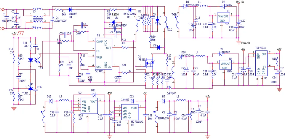
Fig.6 SMPS Circuit Diagram
After selecting the topology that is best suited to the power supply specification, the next choice is to fix the switching frequency and transformer parameters. To do this, it is necessary to know the numerical relation between maximum available power and transformer parameters such as magnetic core area, magnetic length, window area, bobbin area, peak flux density and coil current density.
A. PWM Controller
PWM controller used in this design is UC3845B which control the switching time of MOSFET power switch. It makes efficiency and stability of SMPS higher and at the same time makes the system cost, volume and weight lower [7].This integrated circuit has an oscillator, a temperature compensated reference, high gain error amplifier, current sensing comparator, and a high current totem pole output ideally suited for driving a power MOSFET switch.
The oscillator frequency of this PWM controller is programmed by the values selected for the timing components Rand C. Capacitor C is charged from the 5.0 V reference through resistor Rto approximately 2.8 V and discharged to 1.2 V by an internal current sink.
= 1.72 ∗ =
1.72
8.2 ∗ 1 = 209
is the input frequency of PWM controller and output frequency provided by PWM controller is = 104.5 which used as the switching pulse of
MOSFET switch. The duty cycle of pulse is controlled by the feedback control loop.
B. Transformer Design
The transformer design parameters were selected such that the SMPS could provide outputs according to the specification table given below
TABLEI
OUTPUT CURRENT AND VOLTAGES THROUGH DIFFERENT WINDINGS
Through winding 1 Through winding 2 Through winding 3 Through winding 4 Through winding 5 Output
voltage 15V 8V 8V 12V 18V Output
current 2A 0.5A 0.5A 0.1A 0.1A
So the total Output Power, which we get, is∑( ∗ )≈ 40 . This power supply is designed with efficiency (η) of 80 %. For deliver this much output power with this much efficiency we require our Input Power to be
, =
( %)/100≈50
The minimum Input Voltage, to the transformer is 36Vdc and the maximum Voltage, to transformer is 72Vdc. We choose maximum Duty cycle, to be 0.47 and our sampling frequency, as calculated earlier was 104.5 KHz. R2 33RR1206 C28 100NF R1 3K9 D4 1N4007 C2 4N7 1KV C37 1nF/1KV +C4 100uF/100V C12 4N7 1KV D5 BYV27/200V VDC+ VDC-C19 10nF C33 1nF R12 100K N2 SG3845 COMP 1 FB 2 CS 3 OSC 4 G N D 5 OUT 6 V C C 7 VREF 8 C5 1nF R3
R4 R6 D7
15v R5 TX1D 7 8 R10 5R6 C35 1nF U2 VIN 2 VOUT 1 G N D 5 VIN 3 VIN 6 VIN 7 D8 TX1A 1 2 N5 TL431 2 3 1 R23 1R C36 R25 1R R24 1R +15V N3 1 2 4 3 C21 R11 4K7 R15 4K7 R26 33K C27 100NF R14 15K 9 1 0 R27 3K3 L3B1 D6 15v R13 33R R19 47K C1 4N7 1KV + C14 100uF/35V C41 10UF Q1 IRF530 2 1 3 R17 47R C20 100N L5 C39 0.1uF D12 D11 C22 1NF C40 0.1uF R28 10K C38 0.1uF -15V +3V3 C29 100nF R18 C32 100nF U1 TSP73733 G N D 3 EN 5 IN 1 OUT 2 G N D 6 FB 4 C34 100nF 5 6 C10 0.1uF C11 0.1uF + C9 330UF/35V R7 10K L2 +15V D3 C7 0.1uF + C6 100uF C23 0.1uF D10 BYV27/200V C24 0.1uF D9 1N4007 L4 N4 7805 2 GND VIN 1 3 VOUT C31 0.1uF + C25 100uF R21 10K +5V + C26 100uF C43 10uf U3 MC79L05AC VIN 2 VOUT 1
G N D 5 VIN 3 VIN 6 VIN 7 -5V D13 1N4007 C42 10uf TX1B 3 4 C16 0.1uF D1 BYV27/200V C13 0.1uF D2 1N4007 R22 10K L1 N1 7805 2 GND VIN 1 VOUT 3
ISSN: 2231-5381
http://www.ijettjournal.org
Page 4543
From all these parameters the Primary winding Inductance canbe found using formula
=( ∗ ) ∗
2∗ ∗
which gives = 217µ .
Design transformer is a course of repeating calculation. For cutting down the works of design, Power Integrations Inc. offers a set of Excel table to design the transformer [7]. So according to that Excel table we found our secondary winding turns.
C. Current Sensing Feedback Loop
The SMPS is made such that maximum load is on +15V supply so we have used that section to provide feedback to the PWM controller. The +15V supply is connected to the input of TL431 which is three-terminal adjustable shunt regulator, whose output voltage can be set to any value between Vref
(approximately 2.5 V) and 36 V according to the input supplied. We have used a voltage divider such that the input to TL431 is 2.5V when our supply gives +15V. At this voltage the TL431 is fully short and the optocoupler drives very high current due to which feedback to the UC3845’s FB pin is very high which will cause the output PWM to switch off and the MOSFET will not get triggered and no EMF will be induced in the primary winding. When the +15V falls below 15V then the input to TL431 will fall below 2.5 V and it will get fully shorted but will have some resistance due to which small amount of current will flow through optocoupler and feedback to the PWM controller will be small and it will generate output pulse of high duty cycle to the MOSFET. Similarly when the +15V has supply greater than 15V the PWM will remain switch off and our MOSFET will remains off.
D. Protection
1) Current Protection – UC3845 has an internal current comparator which has a reference of 1V. Whenever input to the CS pin of UC3845 which is other input of CS comparator gets beyond a limit of 1V the output of the IC automatically gets switched off. So we have fed back the CS pin from the MOSFET source through a voltage divider such that the input to the CS pin is less than 1V. If the output supply at secondary sides get shorted than the MOSFET will drive very large amount of current due to which voltage at the CS pin will get above 1V and the UC3845 will stop generating PWM pulses and our SMPS will get switch off and our circuit will remain protected.
2) Snubbers - There are two basic ways to solve the problem of a semiconductor device that is stressed beyond its rating. Either the device can be replaced with a higher rated device to meet the stress level, or a snubber circuit can be added to reduce the stress to a safe level. Both options are trade-offs between cost, availability of the higher rated device, complexity,
component count and the cost of using a snubber circuit. A snubber circuit is typically used to limit the rate of rise of voltage (ΔV/Δt), the voltage applied across the device during turn-off, the rate of rise of current (ΔI/Δt) and the current through the device during turn-on. We have used snubber protection for our MOSFET because when the MOSFET gets switched ON, it gets a very high peck voltage which gets stabilized after some time. To save our MOSFET from this voltage peak we have used a snubber circuit in parallel to MOSFET so that the snubber suppresses the peak and our MOSFET remains protected.
E. Selection of other Components used
The MOSFET that is being used as a switch in this SMPS design is IRF530. This is an N-Channel enhancement mode silicon gate power field effect transistor. This power MOSFET is designed for applications such as switching regulators, switching converters, motor drivers, relay drivers, and drivers for high power bipolar switching transistors requiring high speed and low gate drive power. This MOSFET can be operated directly from IC’s.
Following IC’s have been used to provide different regulated voltages
1) IC7805- This is a positive Voltage regulator which provides an output voltage of +5V when its input ranges from +7 V to +15 V.
2) IC7809- This is a negative Voltage regulator which provides an output voltage of -5V when its input ranges from -7V to -15 V.
3) IC7915- This is a negative Voltage regulator which provides an output voltage of -15V when its input ranges from -17.5V to -30 V.
4) TSP7373- The TPS737xx family of linear low-dropout (LDO) voltage regulators which uses an NMOS pass element in a voltage-follower configuration to provide an output voltage 0f +3.3 V when its input voltage ranges between 2.2 to 5.5V.
V. RESULTS
ISSN: 2231-5381
http://www.ijettjournal.org
Page 4544
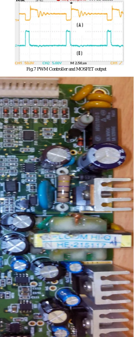
Fig.7 PWM Controller and MOSFET output
Fig.8 Hardware Design
Figure 8 shows the hardware implementation of multiple output SMPS. The next waveforms shown here in, Fig. 9, Fig. 10, Fig. 11, Fig. 12 and Fig 13 are of different output voltages. The different voltage levels obtained can be seen clearly from the respective figures shown below.
Fig.9 Output Voltage (Isolated +5V)
Fig.10 Output Voltage (+15V)
Fig.11 Output Voltage (+5V)
ISSN: 2231-5381
http://www.ijettjournal.org
Page 4545
Fig.13 Output Voltage (+5V)
REFERENCES
[1] Muhammad H. Rashid,”Power Electronics Handbook, Second Edition Devices”, Circuits and Applications,Academic Press.
[2] Abraham I. Pressman, “Switching Power Supply Design,” McGraw-Hill.
[3] Babak Abdi, Jafar Milimonfared, Ahmad Mahin Fallah,”A High-Performance 1.3 KW SMPS with Single Switch Forward Topology”, 9th International Multitopic Conference, IEEE INMIC 2005, pg. 1 – 5. [4] Vishnu P.Nambiar, Azli Yahya and Thayala R. Selvaduray, ”SPICE Modelling of a Valley Switching Flyback Power Supply Controller for Improved Efficiency in Low Cost Devices”, Circuits and Systems (ICCAS), 2012 IEEE International Conference, pg. 10-14
[5] Nasir Coruh, Satilmis Urgun, Tarik Erfidan, “Design and Implementation of Flyback Converters”, Industrial Electronics and Applications (ICIEA), 5th IEEE Conference, 2010, pg. 1189 – 1193. [6] Pressman A.I., "Switching Power Supply Design", Second Ed.
McGraw-Hill, 1998, pp. 105-140.