Published online February 28, 2014 (http://www.sciencepublishinggroup.com/j/ajmp) doi: 10.11648/j.ajmp.20140302.13
Optical, morphological and electrical properties of silver
and aluminium metallization contacts for solar cells
Zakia Fekkai
*, Nazir Mustapha, Ali Hennache
Department of Physics, College of Sciences, Al Imam Mohammad Ibn Saud Islamic University (IMSIU), Riyadh, Saudi Arabia
Email address:
[email protected](Z. Fekkai), [email protected] (N. Mustapha), [email protected](A. Hennache)
To cite this article:
Zakia Fekkai, Nazir Mustapha, Ali Hennache. Optical, Morphological and Electrical Properties of Silver and Aluminium Metallization Contacts for Solar Cells.American Journal of Modern Physics. Vol. 3, No. 2, 2014, pp. 45-50. doi: 10.11648/j.ajmp.20140302.13
Abstract:
A lower resistivity and better spectra selectivity is a measurement of the quality and potential use of silver Ag and aluminium Al metals for the application as metallization contacts for solar cells. Aluminium (Al) and silver (Ag) thin films deposited by thermal evaporation at room temperature were dense with small grain sizes, and maintained a high value of reflectance (in the spectral range from 300 to 3200 nm) with annealing at 300 °C in an argon atmosphere. Experimental results indicate that the surface roughness is increased while the film’s resistivities are reduced. It was also found that the surface roughness and work function of metal films are very important to enhance the stability and efficiency of electrode thin films used for solar cells.Keywords:
Metal Thin Films, Thermal Evaporation, Optical Coatings, Physical Interfaces, Solar Cell Electrodes1. Introduction
In recent years, there has been an increase in the number of applications of Aluminium (Al) and silver (Ag) thin films, due to their unique optical, electrical and mechanical properties which are different to those of bulk materials. These properties have led them to play an irreplaceable and increasing role in many areas of today’s very demanding and rapidly developing technology, especially in the electronic device applications and optical industries [1-3]. The ability to deposit thin films of various materials is important for the fabrication of modern microelectronic devices and for enabling a variety of investigations of fundamental physical principles.
Interest in metal films as contacts in microelectronic devices such as aluminium and silver, has increased for a wide range of applications including heat-reflecting mirrors [4], the field of flat panel displays [5], antireflection coatings [6], organic light-emitting diodes [7], gas sensors [8] and as contact electrodes in solar cells [9]. Silver is used as contact metallization in the microelectronic devices due to its low surface resistivity (1.57 µΩ.cm at room temperature) [10-14] and to its thermal stability. It is believed that Silver has lower resistance than that of Aluminium. Based on these reasons silver Ag is considered to be one of a potential metallization schemes for future integrated circuits (IC's).
Aluminium is a popular metal used to interconnect ICs,
both to make ohmic contact to the devices and connect these to the bonding pads on the chip's edge. Aluminium adheres well to both silicon and silicon dioxide, can be easily vacuum deposited (since it has a low boiling point), and has high conductivity [15].
In general the desired properties for silver and aluminium films used as metallization contacts are as follows:
1- Low specific resistivity. 2- Good thermal stability.
3- High uniformity across the flat substrate. 4- Low particle contamination.
5- Good adherence to substrate. 6- Low manufacturing costs
There are several deposition techniques to grow Al and Ag metal thin films such as magnetron sputtering [16] and evaporation [17]. The resulting Al and Ag films exhibit low resistivity (ca. 4.2 × 10− 4Ω.cm and 1.57 × 10⁻⁶ Ω.cm) respectively and high optical reflectance in the visible region (ca. 90% and 96% ; bandgap, 4. 08 and 4.73 eV respectively), which are to those films deposited on glass substrates [18-20].
to be the operating atmosphere of optoelectronic devices such as solar cell. Moreover, due to the thermal annealing, the surface roughness has increased and also the grain sizes. Furthermore, the films adherence increased but the resistivity decreased for both metals used.
The goal is then to characterize the thermally evaporated aluminium Al and silver Ag thin films used as metallization contacts or cathodes in optoelectronic devices such as solar cells.
2. Experimental Details
A conventional vacuum evaporation system was used in the preparation of Silver and Aluminium films onto cleaned microscope glass substrates in ultrasonic bath with acetone, rinsed with ultra pure de-ionized water for 15 minutes and dried in oven at 120 0C for outgassing. The base pressure prior deposition was approximately 5×10 −6 Torr. The materials used for film preparation were high-purity (99.99%) Al and Ag pellets .The substrates were maintained at room temperature during all sample depositions. The Schematic Diagram of the evaporation system is shown in Figure 1.
The experimental setup for vacuum evaporation consists of a vacuum chamber, vacuum pumps and control panel. The vacuum chamber is closed by glass shade standing on the background by rubber gasket. Inside the chamber, there are substrate holder, wolfram crucible with supply connections, and shutter. The shutter is located between source and substrate and is used to cut off vapour stream from impinging onto the substrate. The thermal evaporation process starts at a relevant vacuum of 5×10 −6 Torr has been attained in the deposition chamber. This process can be divided into three steps [20]:
Sublimation of source generated by high temperature. Transport of vapour towards the substrate.
Vapour condensation and thin film growth on the substrate. (Substrate may be heated to 200-300°C for better adhesion).
The vapours of source material are transported towards the substrate. Molecules of transported material land onto the substrate and form a thin film. If the depositing species or molecules arrival energy is too high they can come back to the vapor to be removed from the chamber by means of the vacuum pumps. This evaporation technology is used to prepare thin films with controlled chemical composition [20-21].
During film deposition, the source-substrate distance was 12 cm and was maintained at the same value for all experiments. A shutter was used to block initial aluminium/ silver evaporating during wetting process. It was above the evaporation source and remove from the line-of sight of depositing species 30 seconds after the start of evaporation. A diffusion pump with a nitrogen trap was used to reduce the vapor pressure of water and prevent back-streaming of oil vapor used in the diffusion pump. Silver Ag and aluminium Al films were deposited with thicknesses ranged from 100
nm to 150 nm usually used in electronic devices and for the precision in comparing morphological, optical and electrical properties of both films. In order to simulate the hostile operation environment of electronic device two sets of samples were prepared. One set of the as-deposited films and the second was annealed for 1 hour in argon gas at a temperature of 300 0C, in order to investigate the changes in thin film properties if any. The surface morphology and roughness were observed using Atomic Force Microscopy (AFM) model (Veeco CT2) in tapping mode. The optical reflectance measurements were performed with a Perkin Elmer Lambda 40 UV/Visible Spectrophotometer.
Figure 1. Schematic diagram of the evaporation system used in metal film deposition.
3. Results
3.1. Optical Properties
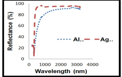
Figure 2 represents the reflectance spectra of both Al and Ag films measured in the wavelength range from 300 nm to 3200 nm of 150 nm thick films. All silver Ag deposited films showed high reflectance slightly over 90% before annealing. While for the aluminium Al films, the reflectance was about 87%. Figure 3 shows the reflectance spectra for the as-deposited Aluminium samples compared to annealed ones at 300 0C in an argon atmosphere. The annealed aluminium Al films showed a slight increase (2-3%) in the reflectance spectrum. For the annealed silver Ag films, the reflectance spectrum was nearly similar to the as-deposited spectrum as shown in Figure 4.
Figure 3. Reflectance spectra of as deposited and annealed at 300 0C Al films measured in the wavelength range from 300 nm to 3200 nm of 150 nm thick films.
Figure 4. Reflectance spectra of as-deposited and annealed at 300 0C silver Ag films measured in the wavelength range from 300 nm to 3200 nm of 150 nm thick films.
3.2. Matlab Interpolation
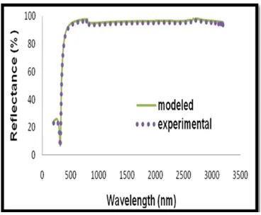
Figure 5 shows the measured and simulated reflectance spectra of the Aluminium thin films (150 nm thick) in the range 600 – 1500 nm. The films showed a reflectance higher than 90% in the visible range. The measured data were then interpolated using MATLAB built-in functions interp [22]. The modeled reflection spectrum of Al thin films deposited on glass is in good agreement with measured data. Figure 6 shows as well similar spectra of the measured and simulated reflectance of the silver thin films. The main goals of the MATLAB modeling process of reflectance spectra for both aluminium and silver metal films were to:
Predict and Track what actually should be the reflectance spectra and determine the improvements if any that must be made to the evaporation process to make these spectra look optimal.
Define the desired evaporation process parameters and how they should be performed to obtain high spectral properties of the metal films.
Maintain the deposition conditions such as current to the crucible, vacuum, deposition time, film thickness and distance to-substrate which, if followed, would lead to the desired film properties.
Figure 5. The modeled/measured reflection spectrum of aluminium Al thin films on glass substrates.
Figure 6.The modeled/measured reflection spectra of silver Ag thin films on glass substrates.
3.3. Atomic Force Microscopy
Atomic Force Microscopy (AFM) was used to evaluate surface roughness and grain sizes of the deposited aluminium Al and silver Ag metal films used as cathodes in the proposed solar cells. The proposed organic solar cell based on glass substrate is illustrated in Figure 7. The organic layer to be used is a new conjugated polymer poly{[2-[2',5'-bis(2"-ethylhexyloxy)phenyl]-1,4-phenylene vinylene]-co-[2-methoxy-5-(2'-ethylhexyloxy)-1,4-phenyle nevinylene]},BEHP-co-MEH-PPV.
Figure 7. A schematic diagram of the organic solar cell.
Since all metal films were deposited at ambient temperature, this may result in voids or defects in the film structure. The annealing was aimed to minimize the voids in the structure of the film. The voids may be due to the high energy of ions landing on the substrate to grow as thin film. Scotch-tape tests were performed to demonstrate good adhesion of the annealed metal film on the glass substrate. The annealed films showed good adhesion to the substrate.
Figure 8. (a) Surface of the as-deposited aluminium Al Film used as a cathode with small grains and (b) and roughness of the film.
Figure 9. (a) Surface of the as-deposited silver Ag Film used as a cathode with small grains and (b) and roughness of the film.
Figure 10. (a) Surface of annealed aluminium Al Film used as a cathode
with small grains and (b) roughness of the film annealed at 300 0C.
Figure 11. (a) Surface of silver Ag Film used as a cathode with small grains and (b) roughness of the film annealed at 300 0C.
3.4. Resistivity
uniform, the resistivity ρ of the films was calculated from the simple equation ρ = Rs d, where d is the film thickness. A
low resistivity of 2.25 × 10− 4Ω·cm and 1.54 × 10− 4 Ω·cm was measured for the 150 nm thick aluminium Al and silver Ag films respectively, at ambient temperature. Typical properties and results obtained for the as-deposited and annealed Aluminium films used as a cathode are presented in Table 1 below. Table 2 shows the typical properties and results obtained for the aluminium Al and silver Ag films, while table 3 shows the typical properties obtained for the as deposited and annealed silver Ag films. The change in the resisitivity of the aluminium Al films with annealing is shown in Figure 12.
Table 1. Typical properties and results measured for the Aluminium Al films.
Property Results (Al)
(as-deposited)
Results (Al) (annealed)
Reflectance (%) 93-94 94-95
Optical Band gap (eV) 3-4.6 3- 4.5
Sheet resistance (Ω / □) 22.5 22.5
Resistivity (Ω.cm) 2.35 ×10⁻⁴ 1.54 ×10⁻⁴
Surface roughness (nm) 7-10 10-15
Grain sizes (nm) 5-6 10-12
Table 2. Typical properties and results measured for the as deposited aluminum Al and silver Ag films.
Property Results (as-deposited) (Al) Results (as-deposited) (Ag)
Reflectance (%) 93-94 96
Optical Band gap (eV) 3- 4.6 4.73
Sheet resistance (Ω / □) 15 10.5
Resistivity (Ω.cm) 2.25 ×10⁻⁴ 1.57 ×10⁻⁴
Surface roughness (nm) 7-10 2.5 nm
Table 3. Typical properties and results obtained for the as-deposited and annealed silver Ag films.
Property Results (Ag)
(as-deposited)
Results (Ag) ( annealed)
Reflectance (%) 94 94
Optical Band gap (eV) 4.73 4.73
Sheet resistance (Ω / □) 10.5 10.5
Resistivity (Ω.cm) 1.57 ×10⁻⁴ 1.57 ×10⁻⁴
Surface roughness (nm) 2.5 2.5
Figure 12. Resisitivity of the aluminum films versus annealing Temperature
The surface roughness and work function properties of metallization films deposited on glass/silicon substrates used in the fabrication of electronic devices are very important to enhance the stability and efficiency of these devices such as solar cell. All functional active layers of the solar cell, which act as injection, transportation and emission layers are deposited onto the substrate, so the surface morphology of substrate is directly transferred to these layers. So uneven interface between the substrate and the solar cell layers is not desirable for the efficiency and stability of cells
4. Molecular Dynamic (MD)
Simulations
Simulation technology has been developed not only to optimize the process conditions efficiently but also to predict the structure profile of the metallization contacts. Therefore, it is necessary to simulate precise profiles by considering the collisions of the evaporated particles with the background gas, the energy of atoms after the emission from the target and the interface between thin film and substrate. Figure 13 shows a computer modeling of a structural zone model for silver coating growth. Computational time restricted the film growth to a two-dimensional growth cell where the film extends in the x direction and grows in the z direction. The energy of the silver vapour was selected to be 1 eV. Thermal energy from annealing helps to minimize the voids and porous structure of the thin films. It also removes defects in the film's microstructure which are due to high energy ions landing on the substrate kept at ambient temperature during the thermal evaporation process.
(a) Thin films with voids in the microstructure.
(b) Heating the substrate improves the thin film quality.
5. Summary
In summary, this paper presents the deposition of highly reflecting and conducting metallization thin films to be used as a cathode electrode of an organic solar cell. A metal thin film with low resistivity (ca. 4.2 × 10− 4 Ω.cm) and high visible-light-reflectance (ca. 90%; bandgap, 3.71 eV) can be achieved on films using a conventional evaporation process, those characteristics are comparable to those of metal films deposited on a glass substrate. The metal films obtained here are applicable to various optoelectronic devices such as solar cells and even organic light emitting diodes.
Super-smooth metal films are particularly desirable for various electronic devices. Annealing the films resulted in reduced optical properties, increased adhesion to substrates, and increasing of surface roughnesses of both films. The adhesion quality of deposited films onto substrates is directly dependent on the cleanliness of the substrate surface.
Smooth and dense aluminum and silver cathodes would enhance their stability, especially when used in long term operation of solar cells.
Acknowledgements
The authors would like to gratefully thank the deanery of academic research at Al Imam Mohammad Ibn Saud Islamic University for the financial support of the project: No.1234-302 301206.
References
[1] Hass G, and Waylonis J E. Optical Constants and Reflectance
and Transmittance of evaporated Aluminum in the Visible and Ultraviolet. J. Opt. Soc. Am. (1961);51(7): 719-22.
[2] Semaltianos N G. Thermally evaporated aluminum thin
films. Applied Surface Science. November 2001; 183(3-4): 223–229.
[3] Lee C -C, Lee T-Y, and Jen Y J. Ion-assisted deposition of silver thin films. Thin Solid Films. (2000); 359(1):95-97.
[4] Volkonen E, Karlsson B. Optimization of metal –based
multilayers for transparent heat mirrors. International Journal of Energy Research. 1987; 11(3): 397-403.
[5] Meiss J, Riede M K, and Leo K. Optimizing the morphology
of metal multilayer films for indium tin oxide (ITO)-free inverted organic solar cells. Journal of Applied Physics. (2009); 105(063108):1-5.
[6] Bouhafs D, Moussi A, Chikouche A and Ruiz J M. Design and simulation of antireflection coating systems for optoelectronic devices. Application to silicon solar cells. Solar Energy Materials and Solar Cells. 16 March 1998; 52(1-2): 79-93.
[7] Hofmann S, Thomschke M, Lussen B and Leo K.
Top-emitting organic light-emitting diodes. Optics Express, (2011); 19(56)1250-1264
[8] Xu J, Shun Y, Pan Q and Qin J. Sensing characteristics of double layer film of ZnO. Sensors and Actuators. (2000); B66 : 161-163.
[9] Yang L, Zhang T, Zhou H, Price S C, Wiley B J and You W.
Solution- processed flexible polymer solar cells with silver nanowire electrodes. American Chemistry Society. Applied Materials and Interfaces. 2011;3(10): 4075-4084.
[10] Hau S-K, O’Malley K-M, Cheng Y -J, Yip H L, Ma H, and
Jen A K-Y. Optimization of active layer and anode electrode for high-performance inverted Bulk-Heterojunction Solar cells. IEEE Journal of selected Topics in Quantum Electronics. Nov/Dec 2010; 16(6):1665-75.
[11] Murarka S P. Multilevel interconnections for ULSI and GSI
era. Materials Science and Engineering: R: reports. 1 May 1997; 19(3-4): 87-151.
[12] Hahn R, Schaffler T, Klockau J and Fotheringham G.
Deposition of Noble metal contacts on YBCO Thin Films. IEEE Transactions on Applied Superconductivity, March 1993; 3(1):2295-2302.
[13] Ono R H et al. Critical current behavior of Ag-coated YBCO
thin films. IEEE Transactions on Magnetics. March 1991; 27(2): 1471-1474.
[14] Alford T L, Nguyen P, Zeng Y, and Mayer J W. Advanced silver-based metallization patterning for ULSI applications. Microelectronic Engineering, March 2001; 55(1-4): 383-388.
[15] Levine Z H, and Ravel B. Identification of materials in Integrated circuit interconnects using X-ray absorption near-edge spectroscopy. Journal of Applied Physics. (1999); 85(558):81-98.
[16] Marechal N and Quesnel E. Silver thin films deposited by magnetron sputtering. Thin Solid Films. Vol. 241. April 1994; 241(1-2): 34-38.
[17] Hwangbo C K, Lingg L J, Lehan J P, Macleod H A, Makous J L
and Kim S Y. Ion assisted deposition of thermally evaporated Ag and Al films. Applied Optics, (1989); 28(14): 2769-78.
[18] Lageeswaran V J et al. Electrical Resistivity and Thermal Stability of Smooth Silver Thin film for Nanoscale
optoelectronic devices. Nanotechnology, 8th IEEE
conference, 2008; 92-94.
[19] Alford T L, Chen L, and Gadre K S. Stability of Silver films on various underlying layers at elevated temperatures. Thin Solid Films, 2003; 429: 248 -254.
[20] Wissmann, P., and Finzel, H.-U. Electrical Resistivity of thin metal films. Berlin Heidelberg, Springer-Verlag, 2007.
[21] Thin Film Processes II. Edited by: Vossen, John L.; Kern, Werner 1991.