1180 | P a g e
THERMOMECHANICAL ANALYSIS OF
ELECTRONIC PACKAGE USING FINITE ELEMENT
METHOD
N.BhargavaRamudu
1, V. Nithin Kumar Varma
2, P.Ravi kiran
3,
T.Venkata Avinash
4, Ch. Mohan Sumanth
5, P.Prasanthi
61,2,3,4,5,6
Department of Mechanical Engineering
Prasad v potluri siddartha institute of technology, Kanuru, Vijayawada (India)
ABSTRACT
This paper deals with the simulation of power electronic components. More precisely it is focused on the modeling approach to emphasize the electro-thermomechanical behavior of materials in power electronics assembly (electronic package). Thermal strains and Stresses constitute an important part of the design considerations for many practical engineering problems. They become especially critical when materials with different coefficients of thermal expansion form interfaces. In this work, an electronic device containing a silicon die (chip), epoxy die attach substrate, and a molding compound is considered for the analysis. A common cause of failure in Electronic devices is the thermal stresses at elevated temperatures caused by a coefficient of thermal expansion mismatch. The present work is focused on the evaluation of the stresses at the interface region at various levels of temperature. The results show that the shear stress magnitude is considerably high compared to other stresses compared to other stresses.
Key Words: Thermal Stress, Electronic Packages, Finite Element Method.
I INTRODUCTION
Power electronic packages (PEP) devices are often exposed to rather insensitive operating conditions such as
high temperatures and these devices consist of different material layers, and each material has different
coefficients of thermal expansion (CTE), which induce thermo-mechanical stresses in each layers under its
operating conditions. Many failure mechanisms in PEM devices were widely reported in the literature [1]. In a
electronic packages, the silicon chip will be attached to die with solder materials to substrate material. The
influence of temperature fluctuations in these assembly during its service time may causes gradual increase of
damage in the structure joints and which leads to failure of the entire assembly. [2] Intensive work is done on
the thermomechanical analysis of electronic packages
Hao peng at al.,[3] presented an advanced, fully nonlinear thermomechanical finite-element model that can
two-1181 | P a g e
phase flow and the heat transfer performance of OHPs using numerail approach. The void effect on the solder
material layers used in power modules subjected to thermal passive cycles are determined by van nahat [4 and
7]. Thermomechanical reliability of polyimide layers in a flip-chip-on-lead-frame dual flat no-leads package
subjected to thermal cycling test condition was studied by the finite element method and the Taguchi method by
wenguo ning at al.,[5]. A novel fatigue life prediction model for electronic components under non-Gaussian
random vibration excitations is proposed based on random vibration and fatigue theory by Yu Jiang et
al.,[6].Thermal mechanical reliability of a hydrogen gas sensor using MEMS-based quartz resonator using finite
element analysis (FEA) is performed by Rui Zhang et al., [8].The main objective of this paper is to present the
implementation such a unified constitutive model in a finite element and its application in power devices. It is
focused on modeling, simulating and analyzing an electronic package. Mechanical characterization of
electronics must be performed in order to ensure that a new system will not fail under normal operation. This is
especially true for systems subjected to high temperatures. An electronic package of silicon die chip is defined
and some simulation results are presented.
II ROLE OF ADVANCED PACKAGING
The approach to electronic packaging has dramatically changed during last decades. In the past, semiconductor
chip, integrated circuit (IC) design was completely separate from the package design. IC was designed first and
then a suitable package selected for assembly. Packages created a standardized set defined with ISO registered
outlines. Advanced IC and package development was mainly driven by military, aeronautics and space
applications, and commercial design rules followed these with reduced requirements. That means the package
type had only a verysmall effect on design and performance on IC.
1182 | P a g e
III THREE- DIMENSIONAL PACKAGING (3D)
Fig-2 below shows three stages of 3D packaging system development. The first stage, creating the system on
package level, is composed of standard package techniques or chips based on combination of film technology
with chips embedded in substrate. Conventional chips and packages are stacked in 3D configuration on basic
substrate and encapsulated. The package to substrate interconnection is usually solder bumps or pad arrays.
Next generation is based on stacking of chips and wafers, where precise alignment is necessary as well as low
temperature bonding. The fundamental operation is forming of vias in single wafers that are thinned to be used
for interconnection of stacked wafers. A future generation configuration is the 3D structure built in Si epitaxial
lateral growth based on low temperature crystallized Si. As evidenced by Fig-3 there is a tendency to
incorporate a significant part of the system in each single level.
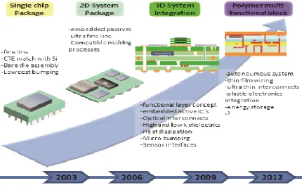
Fig. 2. Integration development of Electronic Packaging [9]
In 3-D packaging some new aspects in the behavior of components have to be predicted, especially in their
interactions. Both single-level, horizontal cross-talk and cross-talk between stacked layers can be a problem,
which may intensify in very high-speed applications. Furthermore, the approach may require use of heat
spreaders in multiple high-power devices to achieve thermal operating specifications as well as thermal and
thermomechanical stress design limits.
The manufacturing process for 3-D microelectronic devices depends on the format chosen for the final product.
Different technologies are used, from challenging semiconductor to the less expensive non-vacuum technology.
1183 | P a g e
interconnects. The elements of dies stacked on edge, layered dies, and a vertically stacked module include dies,
attachments between dies or components and interconnects between dies or modules.
.Fig-3 Three stages of 3D package development[9]
IV MODELING AND GEOMETRY OF PACKAGE (EXAMPLE):
In this model using FEM a standard electronic package is taken which is manufactured up to package level is
analyzed. In the first stage a geometric model of solid 20 node 95 is taken for analysis. In 20 node 95 model
each element is defined by 20 nodes and each node is defined by 3 degrees of freedom.
7.5mm
2mm
1mm
1mm
0.1mm
5mm
Extrude thickness of 10 mm
1184 | P a g e
Table.1 Properties of constituent materials in the electronic package:
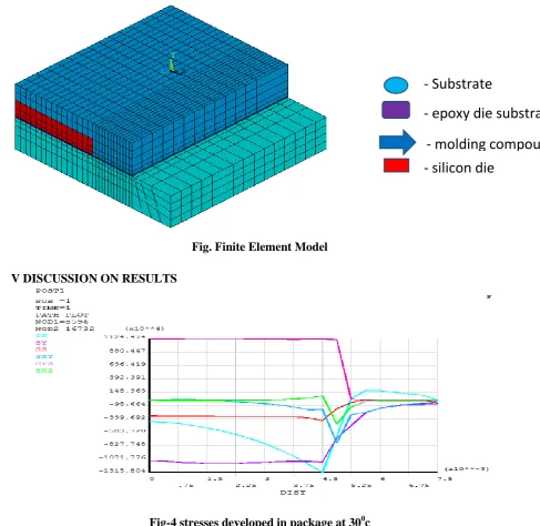
Fig. Finite Element Model
V DISCUSSION ON RESULTS
Fig-4 stresses developed in package at 30
0c
E
(Gpa)
v
Thermal
expansion
coefficient
(10^-6/
oc)
substrate
22
0.39
18
Die attach
7.4
0.4
52
Silicon
163
0.278 2.6
Molding
compound
15
0.25
16
- silicon die
chip
- Substrate
- epoxy die substrate
1185 | P a g e
The finite element models are subjected to different temperatures. The interface stresses are plotted along the
interaction of the epoxy die attach. Compared to all the stresses, the shear stresses are more and these stresses
are decreasing after 5 mm and steady state trend is observed after 5mm.
Die attach which is weakest and having more thermal expansion coefficient readily undergoes deformation and
is more stressed areain the package. Here are some graphs in which package is subjected to various
temperatures from 40-100.
Following figures shows the variation of the same stresses by increasing the temperature of the assembly from
40 to 1000c. the increment of temperature increases the stresses at the interface. From these graphs, it is
observed that the life of electronics packages increases by maintain the assembly at lower temperatures.
TEMPERATURE 80
0c
TEMPERATURE 70
0c
TEMPERATURE 50
0c
TEMPERATURE 60
0c
1186 | P a g e
VI CONCLUSIONS
1. In the above graphs we observe that there is an increasing trend of stresses with temperature.As the
temperature is increasing materials will get more stressed which it is directly proportional to
temperature.
2. The weakest constituent is die attach which is to be more concentrated while designing the package.
3. Among all stresses shear stress xy is more dominating.
4. Design parameters are to be calculated based on the shear stress xy.
REFERENCES
1. C. Mauro, Selected failure mechanisms of modern power modules, Microelectron. Reliab. 42 (2002) 653–
667.
2. P. Rajaguru, H. Lu , C. Bailey , J. Ortiz-Gonzalez , O. Alatise, “Evaluation of the impact of the physical
dimensions and material of the semiconductor chip on the reliability of Sn3.5Ag solder interconnect in
power electronic module: A finite element analysis perspective”, Microelectronics Reliability 68 (2017)
77–85.
3. Hao Peng, P. Frank Pai, , Hongbin Ma, ” Nonlinear thermomechanical finite-element modeling, analysis
and characterization of multi-turn oscillating heat pipes”, 69 (2014) 424–437.
4. Van Nhat Le, Lahouari Benabou ⁎, Victor Etgens, Quang Bang Tao, “Finite element analysis of the effect
of process-induced voids on the fatigue lifetime of a lead-free solder joint under thermal cycling”,
Microelectronics Reliability 65 (2016) 243–254.
5. Wenguo Ning, Chunsheng Zhu , Heng Li, Gaowei Xu , Le Luo , Hongyan Guo c , Fei Jing, “Optimal
design toward enhancement of thermomechanical reliability of polyimide layers in a
flip-chip-on-lead-frame dual flat no-leads package with copper pillar bumps”, Materials Science in Semiconductor
Processing 16 (2013) 933–939.
1187 | P a g e
6. Yu Jiang, J.Y. Tao, Y.A. Zhang , G.J. Yun, “Fatigue life prediction model for accelerated testing of
electronic components under non-Gaussian random vibration excitations”, Microelectronics Reliability 64
(2016) 120–124.
7. F. Arabi, L. Theolier, D. Martineau, J.-Y. Deletage, M. Medina, E. Woirgard, “Power electronic
assemblies: Thermo-mechanical degradations of gold-tin solder for attaching devices”, Microelectronics
Reliability 64 (2016) 409–414.
8. Rui Zhang, Hongbin Shi, Yuehong Dai, Jong Tae Park, Toshitsugu Ueda, Thermo-mechanical reliability
optimization of MEMS-based quartz resonator using validated finite element model, Microelectronics
Reliability 52 (2012) 2331–2335
![Fig. 1. Development of Packages In The Last Decades [9]](https://thumb-us.123doks.com/thumbv2/123dok_us/9261316.1464596/2.595.74.550.471.755/fig-development-packages-decades.webp)