ISSN: 2393-8366
638
Study on Area Efficient Radix-2 FFT Architecture
to Process Twin Data Streams for High Speed Real
Time Application
Anupriya K.P.1,Rachana M.K.2, Manju V.M.3
1PG Scholar, 2,3Assistant Professor,
Department of Electronics Communication Engineering, IES College of Engineering, Thrissur, India. [email protected],[email protected], [email protected]
Abstract: This paper proposes a novel shared multiplier scheduling scheme for area efficient radix-2 FFT architecture to process twin data streams for High speed real time application. In these days many application require simultaneous computation of multiple independent Fast Fourier Transform with its outputs are in natural order. So this paper present a 16 point pipelined FFT processor for FFT computation of two independent data stream. In this N/2 decimation in time FFT and N/2 point decimation in frequency FFT to process the odd and even samples of two data streams separately. This SMSS technique reduce total number of complex multiplier and hardware complexity. The proposed pipelined FFT processor based on SMSS are designed using XILINX ISE TOOL and coded by Verilog HDL language. In addition the proposed processor can be extended to any FFT sizes using additional stages.
Keywords - SMSS, Radix 2 pipelined FFT, DIT and DIF, Multipath delay commutator, Odd and Even samples, MIMO, Xilinx ISE Tool.
1. Introduction
FFT Processor play an important role in OFDM techniques, image processing and signal processing application. Such application require high speed FFT Processor to meet demands for higher data rates. For implementing such processors several architectures are used. They are Memory based, Reconfigurable and Pipelined FFT. Memory based FFT processor [1], [2] are used to achieve small area. Here it use Application specific instruction set processor to meet flexibility for FFT computation. Reconfigurable FFT processors [3] are used to select various FFT sizes on processor so it will reduce hardware complexity. The pipelined processors [4] are used for achieving high throughput rate. Pipelined processors are classified into single path delay commutator (SDC), single path feedback (SPF), Multi path delay feedback (MDF) and multipath delay commutator. This architecture is based on Multipath delay Commutator. MDC architectures provides high throughput rate and simple synchronizing control using multi data path. In MDC Radix size is high then throughput is high.
FFT architectures [5]–[8], In which multiple independent data streams are used. However, all the data streams are processed by a single FFT processor in [5] and [8]. In [8], four independent data streams are processed one by one. Similarly, eight data streams are processed at two domains in [5]. Thus, the outputs of multiple data streams are not available in parallel. In order to simultaneously process the data streams, more than one FFT processors need to be employed. In [6], one to four data streams are processed using multiple data paths for wireless local area network application. Data of different data streams are interleaved to process them simultaneously in [7].
ISSN: 2393-8366
639
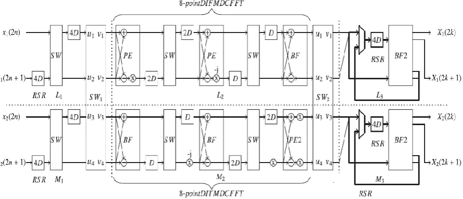
processed by point decimation in time FFT. The even samples are directly processed by N/2-point DIF FFT. So its outputs are bit reversed order. Therefore, the outputs of N/2-N/2-point DIF FFT are bit reversed. Outputs of the two N/2 point FFTs are further processed by the two parallel butterflies to generate the outputs of Npoint FFT in natural order. In FFT computation several multiplications are required. These multiplications are performed by SMSS technique. Here bit reversing is carried out by the scheduling registers. Which are actually used to delay the samples for performing the butterfly operations. Thus, FFT architecture does not use any dedicated circuit to bit reverse the data. Because of this, the proposed architecture requires less number of registers than the prior FFT designs.
2. Fast Fourier Transform
The FFT is an algorithm to speed up the DFT calculation by reducing the number of multiplications and additions required. It has several applications in signal processing. Because of the complexity of the processing algorithm of FFT, now various FFT algorithms are available for processing function and to reduce hardware complexity. Here the FFT processor is to perform 16 points FFT analysis.
The Fourier transform converts information from the time domain into the frequency domain. It is an important analytical tool in such diverse fields as acoustics, optics, seismology, telecommunications, speech, signal processing, and image processing.
There will be two classes of FFT operation 1) Decimation in Time (DIT) Algorithm 2) Decimation in Frequency(DIF) Algorithm
In DIT, The N point DFT of sequence X(n) convert the time domain N point sequence X(n) to Frequency domain N point sequence X(k).In DIT Algorithm the time domain sequence X(n) is decimated and smaller point DFT are performed. The result of smaller point DFTs are combined to get the result of N point DFT.
In DIF, In DIF algorithm the frequency domain sequence X(k) is decimated. In this algorithm the N point time domain sequence is converted to two numbers of N/2 Point sequence. Then each N/2 point sequence is converted to two numbers of N/4 point sequence. Thus we get 4 numbers of N/4 point sequence. This process is continued until we get N/2 numbers of 2 point sequences. Finally the 2 point DFT of each 2 point sequence is computed. The 2 point DFTs of N/2 numbers of 2 point sequences will give N samples, which is the N point DFT of the time domain sequence.
3. Existing 16-Point Radix-2 FFT Architecture
The architecture is designed to process two independent data streams simultaneously with less amount of hardware. The odd inputs, which are in natural order, are first bit reversed and then they are processed by N/2-point decimation in time (DIT) FFT. The eve samples are directly processed by N/2-point DIF FFT, so its output are in bit reversed order. Therefore, the outputs of N/2-point DIF FFT are bit reversed. The outputs of the two N/2-point FFTs are further processed by the two-parallel butterflies to generate the outputs of N-point FFT in natural order. The bit reversing is carried out by the scheduling registers, which are actually used to delay the samples for performing the butterfly operations. Thus, the FFT architecture does not use any dedicated circuit to bit reverse the data. As a result, the proposed architecture requires less number of registers than the prior FFT designs.
ISSN: 2393-8366
640
butterfly operations between the bit reversed data in the RSR in the last stage and outputs from the eight-point DIT FFT. Thus, the upper and lower BF2 in the last stage generate the FFT outputs of the first and the second data streams in normal order.
Figure 1: 16 point rAdix 2 FFT architecture
The two data paths from SW2 are combined together, so the word length of the data path in last stage is twice and so thick lines are used for representing the data paths and registers. The FFT architecture in Fig. 1 is divided into six levels (L1, L2, L3, M1, M2, and M3). The RSR registers in the levels L1 and M1 reorder the odd input data and the RSR registers in the levels L3 and M3 reorder the partially processed even data. The eight-point DIF and DIT FFT operations are performed in the levels L2 and M2, respectively. The data from L1 and M1 can be forwarded to L2 and M2, respectively, or vice versa with the help of SW1. Similarly, the data from L2 and M2 can be forwarded to L3 and M3, respectively or vice versa with help of switch SW2. SW1 and SW2 have two switches (SW) to swap the data path and propagate the data to different levels. During the normal mode, the switches (SW1 or SW2) pass the data at u1, u2, u3, and u4 to v1, v2, v3, and v4, respectively.
However, during the swap mode, the switches (SW1 or SW2) pass the data at u1, u2, u3, and u4 to v3, v4, v1, and v2, respectively. SW1 is in the swap mode during the first N/2 clock cycles and it is in the normal mode during N/2 + 1 to N. On the other hand, SW2 is in the normal mode during the first N/2 clock cycles and it is in the swap mode during N/2 + 1 to N. Thus, SW1 and SW2 are in different modes at any time and change their modes for every N/2 clock cycles. Moreover, if there is transition of data between Ly and L y+1 or My and My+1, then the switches are in the normal mode, and if there is transition of data between L y and My+1 or My and Ly+1, then the switches are in the swap mode. Like other control signals in the design, the control signals to the switches SW1 and SW2 are externally provided and these switch control signals swap at every N/2 clock cycles.
4. Architecture of SMSS Based FFT
ISSN: 2393-8366
641
employ a bit parallel multiplier according to the equation (1), and the circuit diagram is shown in Fig 2.
Output = in * √2 /2 =in * [1+ (1+2-2) (2-6 -2-2)] ---- (1)
The resulting circuit uses three additions and three barrel shift operations.
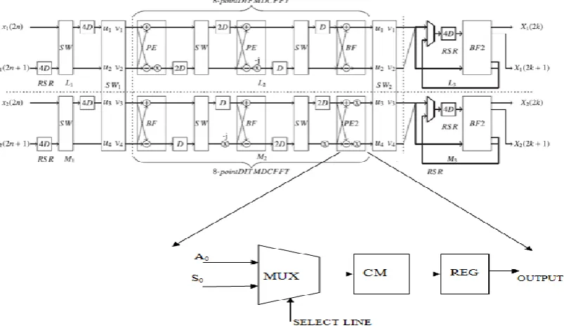
The proposed SMSS Architecture is shown in Fig 3. This method is designed based on Mux working. It consist of delay elements that will Store the required multiplication coefficients.
Figure 2: Circuit diagram of the bit-parallel multiplication by 1/ √2
Figure 3: SMSS Architecture
ISSN: 2393-8366
642
In proposed method, The SMSS technique is applied in PE2 stage of Existing processor. Because both adder and subtractor output is multiplied by 0.707 multiplication coefficient. So The adder and subtractor output of PE2 stage is selected by using shared multiplier scheduling scheme. Then it is multiplied by 0.707 and the output is stored in a register. Therefore by using this technique we can reduce the area, power and time delay of architecture compared to existing processor. The architecture of introduced SMSS based FFT architecture is shown in Fig 4.
5. Conclusion
Here a technique to reduce the area of pipelined FFT architecture is presented. It is designed using Xilinx ISE14.2 Tool. This technique reduce number of complex multiplication and hardware complexity. In which outputs are generated in the natural order. The proposed processor can process two independent data streams simultaneously, Somakes it suitable for many high-speed real-time applications. The bit reversal circuit present in prior designs is eliminated in this technique by integrating two FFT processors. In addition the proposed processor can be extended to any FFT sizes using additional stages.
Acknowledgement
I express my sincere thanks to my guide Ms. Rachana M K for her valuable guidance and useful suggestions, which helped me in the project work.
REFERENCES
[1] S.-J. Huang and S.-G.Chen, “A green FFT processor with 2.5-GS/s for IEEE 802.15.3c (WPANs),” in Proc. Int. Conf. Green Circuits Syst., Jun. 2010, pp. 9–13.
[2] P.-Y. Tsai, T.-H.Lee, and T.-D.Chiueh, “Power-efficient continuous flow memorybased FFT processor for WiMax OFDM mode,” in Proc. Int. Symp.Intell.SignalProcess.commun. Syst., Dec. 2006, pp. 622– 625.
[3] C.-H.Yang,T.-H.Yu Power and area optimization of reconfigurable FFT processors: A 3Gpp- LTE example,’’ IEEE Trans. Very Large Scale Integr. (VLSI) Syst., vol. 47, no. 3, pp. 757– 768, Mar. 2012.
[4] T. Cho and H. Lee, “A high-speed low complexity modified radix- FFT processor for high rate WPAN applications,” IEEE processor for WPAN/WLAN/WMAN systems,” IEEE J. Solid-State Circuits, vol. 47, no. 6, pp. 1419–1435, Jul. 2012.
[5] Y. Chen, Y.-W.Lin, Y.-C.Tsao,and C.-Y. Lee, “A 2.4-Gsample/s DVFS FFT processor for MIMO OFDM communication systems,” IEEE J. Solid-State Circuits, vol. 43, no. 5, pp. 1260– 1273 May 2008.
[6] S.-N. Tang, C.-H.Liao, and T.-Y.Chang, “An area- and energyefficient multimode FFT Architecture” IEEE Trans. Very Large Scale Integr. (VLSI) Syst., vol. 21, no. 1, pp. 187–191, Jan. 2013.
[7] P. P. Boopal, M. Garrido, and O. Gustafsson, “A reconfigurable FFT architecture for variable-length and multi-streaming OFDM standards,” in Proc. IEEE ISCAS, May 2013, pp. 2066–2070.
[8] K.-J. Yang, S.-H.Tsai, and G. C. H. Chuang, “MDC FFT/IFFT processor with variable length for MIMO-OFDM systems,” IEEE Trans. Very Large Scale Integr. (VLSI) Syst., vol. 21, no. 4, pp. 720–731, Apr. 2013.
ISSN: 2393-8366
643
[10] “VLSI Architecture of Shared Multiplier Scheduling Scheme for Reconfigurable FFT/IFFT Processor”T. Ganesh Reddy,International Journal of Research.
[11] A Low-Power 64-point Pipeline FFT/IFFT Processor for OFDM Applications, Chu Yu, Member, IEEE, Mao-Hsu Yen, Pao-Ann Hsiung, Senior Member, IEEE, and Sao-Jie Chen, Senior Member, IEEE.”IEEE Transactions on Consumer Electronics, Vol. 57, No. 1, February 2011”
ABOUT AUTHORS
Ms. Anupriya K.P., currently pursing PG in VLSI Design from IES college
of Engineering, Thrissur, Kerala, India. She received her B.Tech. in Electronics and Communication Engineering from SETCEM college, Thrissur, kerala, India in 2015. Her interested research areas are Signal processing, low power vlsi design and digital system design.
Ms. Rachana M.K., currently working as Assistant Professor in Department
of Electronics and Communication Engineering at IES College of Engineering, Thrissur, Kerala, India. She received her B.Tech. in Electronics and Communication Engineering from Cochin university of Science and Technology in 2005 and M.E degree in VLSI Design from Anna University, Chennai in 2015. Her research interests are VLSI Design and Embedded System Design.
Ms. Manju V.M., currently working as Assistant Professor/PG coordinator in