Emerging Science Journal
Vol. 1, No. 4, December, 2017
Parallel Processor Architecture with a New Algorithm for Simultaneous
Processing of MIPS-Based Series Instructions
Ali Hadizadeh
a*, Ehsan Tanghatari
aa Digital Systems Group, EE Faculty, Sharif University of Technology, Tehran, Iran
Abstract
Processors are main part of the calculation and decision making of a system. Today, due to the increasing need of industry and technology to faster and more accurate computing power, design and manufacture of parallel processing units, has been very much considered. One of the most important processor families used in various devises is the MIPS processors. This processor family had been considered in the telecom and control industry as a reasonable choice. In this paper, new architecture based on this processor, with new parallel processing design, is provided to allow parallel execution of instructions dynamically. Ultimately, the processor efficiency to several fold will be increased. In this architecture, new ideas for the issuance of instructions in parallel, intelligent detection of conditional jumps and memory management are presented.
Keywords:
Parallel Processor; Parallel Alignment;
Intelligent Instruction Prompts; Intelligent Branch Prediction; MIPS Processor.
Article History:
Received: 20 September 2017
Accepted: 30 November 2017
1- Introduction
MIPS processors are a group of processors based on the Reduced Instruction set Computers (RISC). So far, 6 generations have been introduced. Initial versions are based on 32-bit instructions, and in later versions 64-bit support is also added. The efforts of MIPS designers are to make low power processors capable of performing in portable devices. In the 1990s, one of three low-order processors was a MIPS processor. In later versions, support for multi-threading structures has also been added to MIPS architectures. In the R2000 version introduced in 1985, multi-cycle architecture was also added. This goal, through the use of the concept of the pipeline, promoted single-cycle architecture to multi-cycle architecture. For this reason, the processor frequency and, ultimately, CPU performance have increased dramatically. In R3000 version, cache feature added to the MIPS architecture along with the multi-threaded feature. This processor was running at 40 MHz the R4000 processor series was introduced in 1991 with full 64-bit support. Also, the frequency was increased to 100 MHz, which in turn was considered to be a great mutation. But to achieve this frequency, the amount of cache was reduced. The R8000 architecture introduced in 1994 was the first member of the MIPS family to use multi- issue functionality that was able to perform two arithmetic or decimal operations along with two memory operations.
In 2013, the MIPS Warrior family was introduced which was categorized in I and P classes. Class I were introduced with support for 64-bit architecture with high processing and multi threating capability with low power consumption. But the P family was able to support both 32-bit and 64-bit instructions and did not support multi-threading functionality.
MIPS mainstream market is in the telecommunications industry, gaming consoles, Internet modems, and digital TV receivers. For example, Sony alone sold over 300 million units in the first two generations of its game consoles with the R3000 MIPS family. The market capacity of this processor as well as the upgrade need of the processing power, is the main reason for replacing parallel processors instead of single-core processors, these processors have the ability to execute multiple instructions simultaneously, but to use them, the instructions must be rewritten for parallel execution, in this paper, with the proposed algorithm, it is possible to execute traditional instructions on a parallel
*CONTACT: [email protected]
DOI:http://dx.doi.org/10.28991/ijse-01126
processor. Techniques such as conditional jump detection and memory management are also used to increase processing speed. In this paper, we will discuss the different architectures of the MIPS processor in the second section, and then in third section we will present techniques and methods for improving system performance and raising the efficiency of constraints. Then, in the fourth section, we will review the practical evaluation and the results of the implementation of the proposed architecture.
2- Study the Basic Architectures of the MIPS Processors
2-1- Single Cycle Architecture
In a single cycle type processor in one clock cycle, the instruction is loaded from the instruction memory and the information needed to execute that instruction is taken from the register file. Then the logical or mathematical operation required in the ALU is performed and eventually the result is stored in main memory. In other words, an instruction is fully executed per clock cycle.
2-2- Processor Units
Instruction memory: This memory has 128 32-bit rows, each row containing a 32-bit instruction. The instructions are structured as follows:
R Type: These instructions use the data in the register file and send the result to the register file itself. Generally,
these instructions are of a computational type, such as addition and subtraction. These Commands, are containing the source address, the destination in the file, and the code of the function. Jump instructions also contain the destination address or relative address.
I Type: These are real-time instructions that perform the operation with a register data and data from the main
memory and store the result in a single register. Load and Store instructions for the main memory are also in this group.
J Type: The branches instructions are conditional and non-conditional. Which uses real time addressing?
Register file: In the MIPS structure, there are 32 of 32-bit registers as a Register File. The two reading ports, as outputs, each addressed by a 5-bit address bus. In this model, register data are placed at the output after the 5-bit address is applied. There is also a write-up port with 5-bit addressing, which performs storing operations on rising edge of the clock. The first register is also ground hardware.
ALU (Arithmetic Logic Unit): This unit is responsible for performing logical and mathematical calculations on the data and instruction prompts. In this paper, this unit performs 32-bit arithmetic operations.
Main memory: The main memory of the system which also has 32-bit width. Memory capacity is considered to be 128 KB (4000 rows). Which are addressed through 32-bit address lines? In this implementation, memory access is accomplished with a clock cycle delay and writes at the same time in rising edge of clock.
Central controller: This unit is responsible for controlling data flow and coordination of different processor parts. Depending on the type of instruction, source and destination of data, 5 bits of Opcode and sometimes, 5 bits of function type, it generates suitable control signals and coordinates in different parts of the processor.
The worst case with architecture of the single-cycle processor is the passage of data from the stage of fetching an instruction to store in memory which as a result, the time it takes to ensure complete operation is high. Because of this, the frequency of this kind of processor cannot exceed a certain value of about a few megahertz. Because of that, other instructions, effectively, perform with unnecessary delay, also, as side effect of that, the number of instructions executed at the time unit in these systems will be limited.
2-3- Control Hazard Unit
To overcome this problem, it is possible to send needed data to previous stages via forwarding lines, such as the dependence of the answer of a summation to the next load command. However, if there is an instruction such as loading from the memory immediately followed by an associative order, then there is no possibility of forwarding data due to the length of the load path from memory, and we have to apply delay to execute the dependent instructions. The control hazard unit controls connection of specific points at different stages by sampling of control and instruction signals from the various stages in the multi-cycle processor structure. So, without having to waste time, it sends the data that is prepared in the previous cycle to the stage that needs that data.
2-4- Multiple Issue architecture:
The main limitation to the multi cycle structure is in sequential instructions with have no dependencies, so these instructions can perform in parallel, so there is no need to perform them in sequential order. In other words, there is no dependence between the instruction lines. And can be implemented in parallel, in which case the system efficiency can be increased.
To do this, you can combine several executive paths in which the instructions can be executing independently. This solution has some disadvantages over its main advantage, namely, increasing the rate of execution of instructions per unit time. These include increasing power consumption, increasing the complexity of the circuit, the impossibility of filling multiple issues at any cases.
To operate this idea, it's obvious that we need to have a window pointer for the instructions' memory. In these systems, due to the inherent nature of the direction of the execution of the instructions, new types of errors are created that we need to take the necessary decisions to solve and handle them. In our study, there are four executive paths, which include two paths for performing arithmetic and logical operations and two paths for loading and storing in main memory. The depth of the lines will be 4 stages, but the depth of the loading path of memory is 5 stages due to the inherent delay of the 5 cycle memory instructions. In this paper, a new method is introduced to address these types of dependencies and resolve them dynamically.
To examine the likelihood of dependency between the window instructions, we consider the slider window with 4 instructions length. Now, depending on the type of instructions, the address of source and destination, the necessary decisions will be made.
In the next step, the structure of the register file should be slightly changed. In the register file, we will need parallel loads. But the number of ports of writing will be two. The reason for this constraint is a steady increase in register file [3, 4].
In the parallel structure, despite the limit on the number of writing ports in the register file (two ports), it is still possible to fill in 4 multiple issues for executing instructions. In this way, there are two lines for arithmetic and branch operations, a storing line and a line to load from the main memory. The path to storing in memory does not require a register write port, and the loading path from memory will also delay the demand for access to the file with a clock cycle, so at one moment all four issues can be filled with a register file with two writing ports.
3- Upgrades the MIPS-Based Multi-Lane Processor
Given the proposed multi-lane structure, there are two ways to execute instructions so that we can use multiple issues. 1- Optimizing the code according to the structure of the processor by the programmer. 2- Optimization of the code by hardware units. Since the recoding of all existing applications for this processor is not possible, it is possible to manage the instructions in real time by adding new hardware units.
3-1- Study of Structural Constraints and Dependency of Instructions for Hardware Recoding
1. Lack of enough ports for writing in the register file: Having 4 executive lines mentioned before, all paths except
store path in the memory requires a writing port in the register file. Consequently, due to having two writing ports in the register file, if all three executed path 1, executive 2 and load from memory want to store something in the register file, a structural hazard will appear.
2. Type of executive instructions: in this processor due to the type of execution paths, two R-type instructions, a
Load instruction and a Store instruction of the memory is executable at any moment of time. For example, if three register instructions exist, inevitably, the third instruction should be entered into pipeline at the next clock.
3. Conditional branch instructions management: to reduce structural complexity, conditional branch instruction
4. Manage instructions that need the result of the load instruction: these instructions are due to the asymmetric structure of executive paths cannot be executed at the same time or with a gap window, they should be at least two spaced apart which can be executed with data forwarding.
5. Manage instructions other than load from memory: in the case of dependency beside the load instruction, the
data of all other instructions could be forwarded if the instructions are fetched in two separate windows.
3-2- Suggested Solutions for Managing Constraints
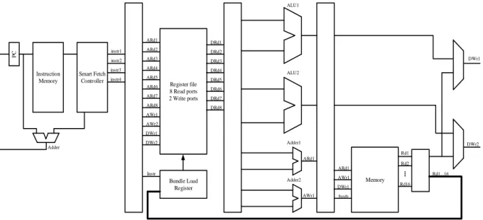
To manage the constraints mentioned in the previous part, some blocks were added to the layout which according to the simulations will improve the processor performance. Figure 1 is a block diagram of our proposed parallel processor.
Instruction Memory
PC
Register file 8 Read ports 2 Write ports Smart Fetch Controller Memory ALU1 ALU2 Adder1 Adder2 ARd1 ARd2 ARd3 ARd4 ARd5 ARd6 ARd7 ARd8 AWr1 AWr2 DWr1 DWr2 DRd1 DRd2 DRd3 DRd4 DRd5 DRd6 DRd7 DRd8 ARd1 AWr1 DWr1 Bundle Load Register Rd1 Rd2 Rd16 Bundle ... DWr1 DWr2 Adder ARd1 AWr1 Rd1...16 Instr instr1 instr2 instr3 instr4
Figure 1. Parallel processor architecture.
3-3- Smart Fetch Controller Block
In this part we will study the most important part of this processor. As explained previously, all the complexities created by parallelizing the processor structure to the single-lane architecture are integrated in this block and other parts consist of execute and write back in register file have simple structure. So the smart block should check the instructions delivered from the instruction memory, control two main constraints, dependency of instructions and the structural constraint of the processor and if possible to fetch the instructions, transmit them to the relevant executive path. The functionality of the block above is to eliminate structural constraints and dependency of instructions can be categorized in below order.
1. Managing the constraint of register file write port and executive lanes: Load instruction from memory require a write port in register file after four clocks. As the result, if three instructions are fetched at the same time and filled up two executive and load lanes, these three instructions can be easily written in the register file but in the next window utmost one R-type instruction can be fetched, because load instruction in previous window will take one of the write port shares. For this reason, we will discuss the idea of token. In this idea, we act in this way that each window should recharge the tokens of load, store and R-type instructions of the next window. Regularly, in each window, one load token, a store token and two R-type token (according to the processor structure) are being recharged. If a load instruction is fetched in this window, the Smart Fetch block will get only one R-type token to the next window. As the result, with the token idea, the problem of few register file write ports and also the limitation of processor lanes is solved.
2. Managing dependency of instructions: in order to recognize and manage dependency of instructions, a table is given which contains the required information for decide on the fetch of instructions.
Table 1. Window checking structure of dependency of instruction.
R1 R2 R3 Type of command
Load Instr. from previous window
First instruction of the window
Second instruction of the window
Third instruction of the window
In the above table, R1 is the register of Rd in R-type instructions and Rt in I-type instructions. R2 is the register of Rs and R3 is register of Rt in the R-type instructions or 0 in I-type. In the last column, the type of instruction for R or I is either zero or one respectively.
Managing multiple types of instruction dependencies should be done using the table above.
1. Target addresses in R1 should not be the same because it may occur error of write after write due to their execution in the same time.
2. R2, R3 in each block should not be the same with any of R1 in the above because a data will be required that has not been produced yet.
Above table and comparisons would guarantee execution of instructions without any problem. After specifying the maximum executable instructions, the PC pointer will increase to the number of fetched instructions in order to fetch new instructions in the next clock. The most important advantage of this design is its scalability. With a larger table, more entries and also the number of token recharged in each clock the number of processor lanes could be increased.
3-4- Conditional Branch Management Block
Pre-determined conditional branch: In some programs, conditional instruction is used for jump between different program lines, in this way the conditional branch is always taken. For example, in a branch instruction which the value of Rt and Rs is equal, this branch is always taken. But in the cycle of processor execution, this may be considered as not taken first as the default branch prediction may be always not taken. Then the pipeline would fill with instructions after the branch instead of its destination. So with hardware designed in fetch and decoding units, the jump instruction in form of branch is properly managed.
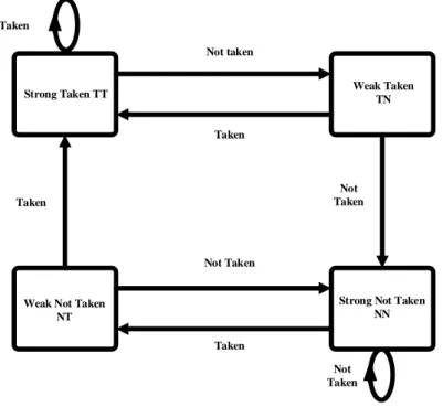
Dynamic Branch Prediction: considering a two-bit shift register for each branch instruction as a conditional branch record according to the state machine below would predict up to 95% of branch results accurately. The processor due to the 2 bits in the shift register would consider a situation for branch and according to this decision, select a guessing destination for fetching new instructions and fills up pipeline with these instructions. when the actual branch result was determined, if this decision was right, shift register will update and it continues to work, and if this decision is wrong, the processor evacuated the pipeline from wrong instruction and begin to fetch instruction from right destination and finally shift register records will update. An overview of the decision –making process can be seen in Figure 2.
Strong Taken TT
Weak Not Taken NT
Weak Taken TN
Strong Not Taken NN Not taken
Taken
Taken Not Taken
Not Taken Taken
Taken
Not Taken
Figure 2. Diagnostic diagram of condition branches.
4- Implementation and Compare Results
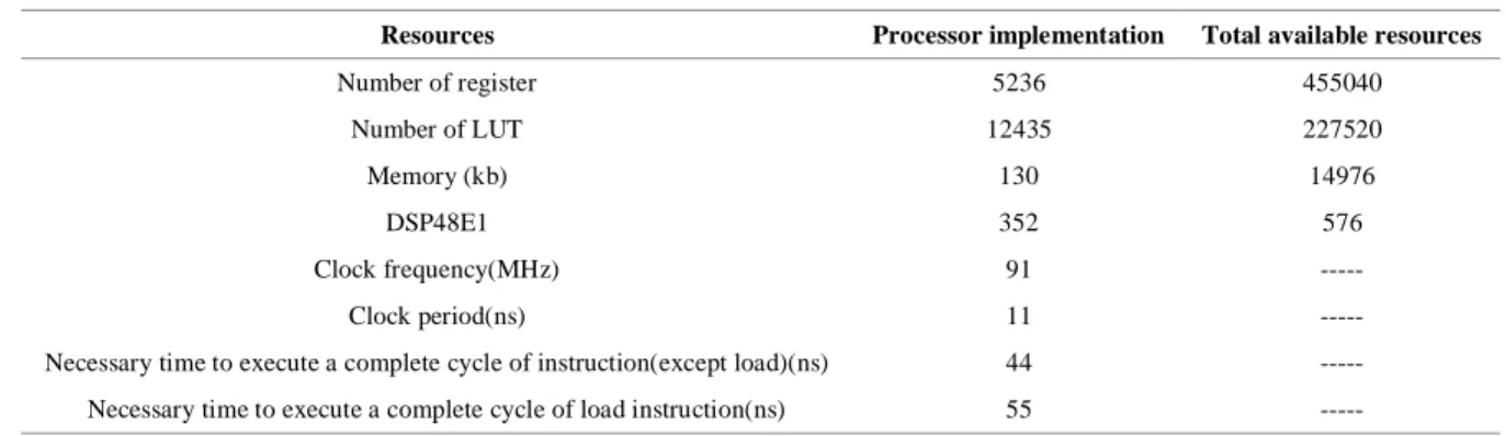
Proposed processor has been implemented on FPGA for testing and ensuring the correctness of the operation. An FPGA from Vertix6 family XCVLX365T has employed. Table of consumed and available resources is shown in Table 2.
Table 2. Consuming table and total available sources of FPGA.
Total available resources Processor implementation
Resources
455040 5236
Number of register
227520 12435
Number of LUT
14976 130
Memory (kb)
576 352
DSP48E1
--- 91
Clock frequency(MHz)
--- 11
Clock period(ns)
--- 44
Necessary time to execute a complete cycle of instruction(except load)(ns)
--- 55
Necessary time to execute a complete cycle of load instruction(ns)
For testing processor and assessing the impact of changes that has been applied, the known test bench “isort32” has run on the processor in multi-cycle mode, multi-lane and finally improved multi-lane. The result of this study is shown in Table 3.
Table 3. Processor efficiency in different architectures.
Improved multi-Lane processor Multi-Lane processor
Multi-cycle processor
10,034 23,372
37,127 Number of required cycle for execute the code
110,374 275,092
408,397 Execute time code
3,7 1,59
--- Speed up over multi-cycle
2,3 ---
--- Speed up over simple multi-lane
Assembly instructions of serial processor are given in the appendix I.
5- References
[1] W. Hu "Godson-3B: A 1 GHz 40 W 8-Core 128GFLOPS processor in 65 nm CMOS" IEEE ISSCC Dig. Tech. Papers pp. 76-78 2011.
[2] Dodd, P.E., and L.W. Massengill. “Basic Mechanisms and Modeling of Single-Event Upset in Digital Microelectronics.” IEEE Transactions on Nuclear Science 50, no. 3 (June 2003): 583–602. doi:10.1109/tns.2003.813129.
[3] C. Carmichael "Correcting single-event upsets in virtex-4 fpga configuration memory" in XAPP 197 Xilinx Inc. 2001.
[4] Azambuja, José Rodrigo, Samuel Pagliarini, Lucas Rosa, and Fernanda Lima Kastensmidt. “Exploring the Limitations of Software-Based Techniques in SEE Fault Coverage.” Journal of Electronic Testing 27, no. 4 (April 9, 2011): 541–550. doi:10.1007/s10836-011-5218-7.
[5] Fan, Bao-Xia, Liang Yang, Jiang-Mei Wang, Ru Wang, Bin Xiao, Ying Xu, Dong Liu, and Ji-Ye Zhao. “Physical Implementation of the 1GHz Godson-3 Quad-Core Microprocessor.” Journal of Computer Science and Technology 25, no. 2 (March 2010): 192–199. doi:10.1007/s11390-010-9316-2.
[6] Lima, F., L. Carro, R. Velazco, and R. Reis. “Injecting Multiple Upsets in a SEU Tolerant 8051 Micro-Controller.” Proceedings of the Eighth IEEE International On-Line Testing Workshop (IOLTW 2002) (n.d.). doi:10.1109/olt.2002.1030217.
Appendix I
Assembly instructions for iSort32:
[0x000000] 0x34080000 # ori $t0, $zero, 0 ($t0 = $zero | 0) [0x000004] 0x24090060 # addiu $t1, $zero, 96 ($t1 = 96)
[0x000008] 0x3403DEAD # ori $v1, $zero, -8531 ($v1 = $zero | -8531) [0x00000C] 0xAD030080 # sw $v1, 128($t0) (mem[$t0 + 128] = $v1) [0x000010] 0x2129FFFF # addi $t1, $t1, -1 ($t1 = $t1 + -1) [0x000014] 0x25080004 # addiu $t0, $t0, 4 ($t0 = $t0 + 4) [0x000018] 0x00631020 # add $v0, $v1, $v1 ($v0 = $v1 + $v1) [0x00001C] 0x00621026 # xor $v0, $v1, $v0 ($v0 = $v1 ^ $v0) [0x000020] 0x3843BEEF # xori $v1, $v0, -16657 ($v1 = $v0 ^ -16657) [0x000024] 0x1409FFF9 # bne $t1, $zero, -7 (if ($t1 != $zero) goto -7) [0x000028] 0x20080004 # addi $t0, $zero, 4 ($t0 = 4)
[0x00002C] 0x20090060 # addi $t1, $zero, 96 ($t1 = 96) [0x000030] 0x01294821 # addu $t1, $t1, $t1 ($t1 = $t1 + $t1) [0x000034] 0x01294821 # addu $t1, $t1, $t1 ($t1 = $t1 + $t1)
[0x000038] 0x0109502A # slt $t2, $t0, $t1 (if ($t0 < $t1) $t2 = 1 else $t2 = 0) [0x00003C] 0x1140000E # beq $t2, $zero, 14 (if ($t2 == $zero) goto 14)
[0x000040] 0x00085820 # add $t3, $zero, $t0 ($t3 = $t0)
[0x000044] 0x8D0C0080 # lw $t4, 128($t0) ($t4 = mem[$t0 + 128])
[0x000048] 0x000B502A # slt $t2, $zero, $t3 (if ($zero < $t3) $t2 = 1 else $t2 = 0) [0x00004C] 0x11400007 # beq $t2, $zero, 7 (if ($t2 == $zero) goto 7)
[0x000050] 0x216DFFFC # addi $t5, $t3, -4 ($t5 = $t3 + -4) [0x000054] 0x8DAE0080 # lw $t6, 128($t5) ($t6 = mem[$t5 + 128])
[0x000058] 0x01CC502B # sltu $t2, $t6, $t4 (if ($t6 < $t4) $t2 = 1 else $t2 = 0) [0x00005C] 0x11400003 # beq $t2, $zero, 3 (if ($t2 == $zero) goto 3)
[0x000060] 0xAD6E0080 # sw $t6, 128($t3) (mem[$t3 + 128] = $t6) [0x000064] 0x000D5820 # add $t3, $zero, $t5 ($t3 = $t5)
[0x000068] 0x1000FFF7 # beq $zero, $zero, -9 (if ($zero == $zero) goto -9) [0x00006C] 0xAD6C0080 # sw $t4, 128($t3) (mem[$t3 + 128] = $t4)
[0x000070] 0x21080004 # addi $t0, $t0, 4 ($t0 = $t0 + 4)