Research Article
a
April
2018
Special Issue: National Conference on Emerging Trends in Engineering 2018
Conference Held at Sri Venkatesa Perumal College of Engineering & Technology, Puttur, A.P., India
Computer Science and Software Engineering
ISSN: 2277-128X (Volume-8, Issue-4)
VLSI Design of Carry Select Adder Using Redundant
Encoding Technique for Arithmetic Calculations
P. Lokesh1, K. Mandal2
1.
Assistant Professor, VEMU Institute of Technology, P.Kothakota, Andhra Pradesh, India
(e-mail: [email protected])
2.
Assistant Professor, VEMU Institute of Technology, P.Kothakota, Andhra Pradesh, India
(e-mail: [email protected])
Abstract— Carry Select Adder (CSLA) is one of the best adders used in many data-processing processors to perform fast arithmetic functions. From the structure of the CSLA, it is obvious that there is possibility for reducing the area and power consumption in the CSLA. CSLA is used in numerous computational systems to ease the problem of carry propagation delay by autonomously generating multiple carries and then select a carry to produce the sum. However, the CSLA is not area competent because it uses several pairs of Ripple Carry Adders (RCA) to generate partial sum and carry by in view of carry input Cin=0 and Cin=1, then the final sum and carry are selected by the multiplexers . Due to the fast growing mobile industry not only the faster arithmetic unit but also less area and low power arithmetic units are needed. Since the CSLA suffering with Redundancy problem this paper presented a novel technique to eliminate all the redundant logic operations present in the traditional CSLA and proposed a new logic formulation for CSLA. In the proposed scheme, the carry select (CS) operation is scheduled before the calculation of final-sum, which is unlike from the conventional approach. Bit patterns of two anticipating carry words (corresponding to Cin = 0 and 1) and fixed Cin bits are used for logic optimization of CS and generation units. An efficient CSLA design is obtained using optimized logic units. The proposed CSLA design involves considerably less area and delay than the recently proposed BEC-based CSLA. Due to the small carry-output delay, the proposed CSLA design is a good entrant for square-root (SQRT) CSLA. The proposed design is simulated, synthesized and verified by Xilinx tools along with Virtex – 5 FPGA board.
Index Terms — RCA, CSLA, Square-root CSLA, Xilinx tools and Virtex -5 FPGA.
I. INTRODUCTION
Adders are of essential substance in a wide variety of digital systems. Many fast adders exist, but adding fast using low area and power is still challenging. The importance of a fast, low-cost binary adder in a digital system is difficult to miscalculate. Not only are adders used in every arithmetic operation, they are also needed for computing the physical address in virtually every memory fetch operation in most modern CPUs. Ripple adders are the smallest but also the slowest. More recently, carry-skip adders, Carry-look-ahead and carry-select adders are very fast but far larger and consume much more power than ripple or carry-skip adders In the case of digital adders, the speed of addition is inadequate by the time required by the carry to propagate through the adder which is known as propagation delay time. The sum for each bit in an adder is generated in succession only after the preceding bits have been summed and a carry is obtained to the next position. The carry select adder is used in many digital computational systems to reduce the difficulty of propagation delay. It can be done by in parallel generation of multiple carries and then select a carry to generate the sum.
Yet, the CSLA is not competent in the case of area because it uses multiple pairs of Ripple Carry Adders (RCA) to generate partial sum and carry by considering carry input Cin=0 and Cin=1 alone, then the final sum and carry are selected by the multiplexer . In the case of MCSLA the basic idea is to use Binary to Excess-1 Converter (BEC) instead of RCA with Cin = 1 in the regular CSLA to achieve lower area and power consumption The main benefit of this BEC logic comes from the lesser number of logic gates than the n-bit Full Adder (FA) structure.
Practical studies are observed that logic optimization largely depends on ease of use of outmoded operations in the formulation, whereas adder delays mainly a function of data dependence. In the active designs, logic is optimized without giving any contemplation to the data dependence. Hence it is proposed to make an examination on logic operations involved in conventional and BEC-based CSLAs to swot the data dependence and to identify redundant logic operations. Based on this examination, a logic formulation for the CSLA can be suggested. The main role in this concern is to formulae logic based on data dependence and optimized carry generator (CG) and CS design.
ISSN(E): 2277-128X, ISBN: 978-93-87396-07-4, pp. 132-136 II. DESIGN DEVELOPMENT
To promote low power high performance applications of computing architectures, various high speed Techniques are modeled on VLSI. The VLSI architecture for the proposed method has implemented as follows.
It is very familiar that the CSLA has two major entities and they are sum and carry generator unit (SCG) and the sum and carry selection unit. The SCG unit consumes most of the logic utilities of CSLA and considerably contributes to the critical path. Meanwhile various logic designs have been recommended for competent execution of the SCG unit. Therefore certain exercise is needed before implementing the techniques to the practical world. The main intention of this exercise is to recognize the redundant logic operations and data dependence. As a result, we eliminate all redundant logic operations and sequence logic operations based on their data dependence.
TABLE 1 SUMMARY OF DESIGN CONSIDERATIONS
Sno Design consideration Selection
1 Compiler Xilinix14.4Vivado
2 Programming Language Verilog
3 FPGA Virtex -5
4 Interface USB
Modeling of proposed csla to overcome redundancy Conventional CSLA:
Figure1: Conventional CSLA
The conventional CSLA is shown in the figure1in which the Sum Carry Generation unit consists of two n-bit RCAs, where n is the adder bit-width. The logic implementation of n-bit RCA is performed in four stages: 1) half-sum generation (HSG); 2) half-carry generation (HCG); 3) full-sum generation (FSG); and 4) full carry generation (FCG). Assume that two n-bit operands are added in the conventional CSLA, then RCA-1 and RCA-2 generate n-bit sum (s0 and s1) and output-carry (c0 out and c1 out) corresponding to input-carry (Cin = 0 and Cin = 1), correspondingly and whose logic expressions are shown in figure2.
Figure2: Logic Expressions of Conventional CSLA-SCG
ISSN(E): 2277-128X, ISBN: 978-93-87396-07-4, pp. 132-136
Figure3: proposed CSLA with removal of Redundancy
The proposed logic expressions are shown in figure3
Front-End Modeling:
This phase of implementation contains the following stages simulation using Xilinx 14.4 Vivado suite, synthesis using Xilinx 14.4 XST and verifying on Virtex – 5 FPGA board.
Figure4: Logic Expressions of proposed architecture
III. SIMULATION AND SYNTHESIS RESULTS
The Verilog RTL Description of the above article is simulated and synthesized using Xilinx14.4 (ISE-Simulator), implementation of all the above proposed techniques are successfully synthesized and verified on Virtex -5 FPGA board and the results are shown below.
ISSN(E): 2277-128X, ISBN: 978-93-87396-07-4, pp. 132-136
Figure6: Synthesis output of proposed CSLA
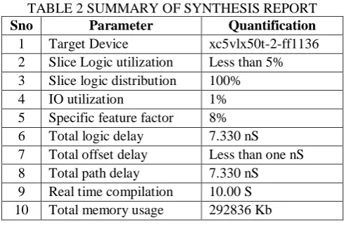
The Synthesized report is summarized in the following Table2.
TABLE 2 SUMMARY OF SYNTHESIS REPORT
Sno Parameter Quantification
1 Target Device xc5vlx50t-2-ff1136
2 Slice Logic utilization Less than 5%
3 Slice logic distribution 100%
4 IO utilization 1%
5 Specific feature factor 8%
6 Total logic delay 7.330 nS
7 Total offset delay Less than one nS
8 Total path delay 7.330 nS
9 Real time compilation 10.00 S
10 Total memory usage 292836 Kb
IV. CONCLUSION
In this paper, proposed a new logic formulation for the CSLA. In the projected system, the CS operation is planned before the calculation of final-sum, which is altered from the conventional approach. Carry words equivalent to input-carry „0‟ and „1‟ generated by the CSLA based on the proposed system follow a specific bit pattern, which is used for logic optimization of the CS unit. Fixed input bits of the CG unit are also used for logic optimization. Based on this, significantly reduced design for CS and CG units are obtained. Using these optimized logic units, an competent design is obtained for the CSLA. The proposed CSLA design involves significantly less area and delay. This paper has realized with Xilinx tools along with Virtex -5 FPGA. Such designs are suggested to exhibits a competitive performance with current work.
REFERENCES
[1] Area–Delay–Power Efficient Carry-Select Adder Basant Kumar Mohanty, Senior Member, IEEE, and Sujit
Kumar Patel
[1] K. K. Parhi, VLSI Digital Signal Processing. New York, NY, USA:Wiley,1998.
[2] A. P. Chandrakasan, N. Verma, and D. C. Daly, “Ultralow-power electronics for biomedical applications,”
Annu. Rev. Biomed. Eng., vol. 10, pp. 247– 274, Aug. 2008.
[3] O. J. Bedrij, “Carry-select adder,” IRE Trans. Electron. Comput., vol. EC-11, no. 3, pp. 340–344, Jun. 1962. [4] Y. Kim and L.-S. Kim, “64-bit carry-select adder with reduced area,” Electron. Lett., vol. 37, no. 10, pp. 614–
615, May 2001.
[5] Y. He, C. H. Chang, and J. Gu, “An area-efficient 64-bit square root carryselect adder for low power application,” in Proc. IEEE Int. Symp. Circuits Syst., 2005, vol. 4, pp. 4082–4085.
[6] B. Ramkumar and H.M. Kittur, “Low-power and area-efficient carry-select adder,” IEEE Trans. Very Large
Scale Integr. (VLSI) Syst., vol. 20, no. 2, pp. 371–375, Feb. 2012.
[7] I.-C. Wey, C.-C. Ho, Y.-S. Lin, and C. C. Peng, “An area-efficient carry select adder design by sharing the
ISSN(E): 2277-128X, ISBN: 978-93-87396-07-4, pp. 132-136
[8] S.Manju and V. Sornagopal, “An efficient SQRT architecture of carry select adder design by common Boolean
logic,” in Proc. VLSI ICEVENT, 2013, pp. 1–5.
[9] B. Parhami, Computer Arithmetic: Algorithms and Hardware Designs, 2nd ed. New York, NY, USA: Oxford
Univ. Press, 2010.
AUTHORS
P.Lokesh received his B.Tech degree in Electronics & Communication Engineering from Yogananda Institute of Technology and Science, Tirupati (A.P), India, in the year 2013. M.Tech degree in VLSI System Design at Chadalawada Ramanamma Engineering College,Tirupati(A.P), Indiain the year 2015.Currently working as a Assistant Professor in VEMU Institute of Technology, P.Kothakota. His area of research Includes Low power VLSI design, Embedded systems.
Mr.K.MANDAL, Assistant Professor, Department of CSE, VEMU Institute of Technology. He has