A Static Time Analysis of 1-bit to 32-page SCA architecture for Logic Test
K.Surya Kumari , Sneha.M.Joseph, V.N.M.Brahmanandam.K,Asst.Prof, Dept of ECE, M Tech Scholar,Asst.Prof, Dept of ECE Pragati Engg College, Surampalem
Abstract— This research proposes the Static Time Analysis of 32 page Single cycle access (SCA) architecture for Logic test. The timing analysis of each and very path of Logic test are observed that is setup and hold timings are calculated. It also eliminates the peak power consumption problem of conventional shift-based scan chains and reduces the activity during shift and capture cycles using Clock-Gating technique. This leads to more realistic circuit behavior during at-speed tests. It enables the complete test to run at much higher frequencies equal or close to the one in functional mode. It will be shown, that a lesser number of test cycles can be achieved compared to other published solutions. The test cycle per net based on a simple test pattern generator algorithm without test pattern compression is below 1 for larger designs and is independent of the design size. The structure allows an additional on-chip debugging signal visibility for each register. The method is backward compatible to full scan designs and existing test pattern generators and simulators can be used with a minor enhancement. It is shown how to combine the proposed solution with built-in self-test (BIST) and massive parallel scan chains. The results are observed on Xilinx XC3s1600e-5fgg484
Index Terms—At-speed testing, low-power testing, on-chip signal visibility, Clock-Gating, BIST, XC3s1600e-5fgg484.
I. INTRODUCTION
HE production test costs of chips become more and more dominant. The standard shift scan (SS) method is the most popular test implementation within the last decades. It hasbeen tried to improve this approach in terms of test time, test data volume and test power by optimizing the scan pattern, more using logic, or a combination of these modifications. Automatic test pattern generation (ATPG)for sequential VLSI circuits is an NP-complete problem with an exponential complexity. The complexity of
combinatorial logic varies. Less complex logic is tested within a few capture cycles, generating an immense number of don’t cares during the rest of the test, even when test compression methods are used. Complex and hard to test logic needs to be stimulated and captured quite often but the pattern need to be shifted throughout the complete scan chain. One approach to reduce test time is to use parallel scan chain. This leads to a massive increase of parallel scan chains to reduce the length of the scan chains. In order to further reduce test data volume, a built-in-self-test (BIST) mechanism.
Another critical aspect of SS implementations is at-speed testing. The high peak power during shift leads to an excessive current due to high switching activity, which can lead to a mis-classification of the circuit-under-test (CUT). This is demonstrated by Sde-Paz et al. in [11].
The pattern reduction for at-speed tests is proposed by Pomeranz by test compaction based on non-scan test sequences and the removal of transfer sequences.
The problem of a slow global scan enable signal in SS is discussed by Ahmed et al. in [13] and solved by implementing a pipelined global scan enable tree. However, none of the methods fundamentally solve the problem of high switching activity, a high number of test cycles and a slow global scan enable signal simultaneously.
The aspects test power, test data volume and test time can be simultaneously reduced with a modified hardware structure known as random access scan (RAS). The enhanced hardware allows the read and write of selected registers or set of selected registers, which reduces the power problems during shift and test time. Based on the initial idea in 1980 by Ando [14], three major groups of RAS schemes can be found.
volume and test application time can be reduced. Lin et al. [16] present a two phase approach how to optimize the pattern based on bit flipping. A test pattern generation scheme based on segment fixing counter reseeding is demonstrated in [17]. However, the fact that each cell needs to be accessed individually generates an unaffordable routing overhead.
The second group addresses each register individually byusing an X (or row) and a Y (or column) address decoder with an additional combinatorial element (for instance AND gate) per register cell. The cell values can be individually read by an additional signal driven by a tri-state logic added to each register cell. Hu et al. propose a variable-to-fixed run-length decoding technique applied on RAS in [18] and a clustered RAS structure in [19]. A modified T-Flip-Flop is shown in [20] to allow the overlap of the test response read out with the loading of the next test input patterns within the same memory addressing cycle. A very similar modified scan register is proposed by Mudlapur et al. in [21] to reduce area overhead of the RAS. However, these proposals have in common, that the x- and y-line select routing is unaffordable, the individual register cells are enhanced by multiple logic elements which generates an unaffordable area overhead and the readout is done using tri-state logic. The third group uses a row decoder and a column decoder to address individual registers. Additionally the read/write mechanism is enhanced with two signals per column, driven by a tri-state driver, connected to the internal latch cells of the registers via tri-state logic and an individual sense amplifier per column. Different variations are discussed. Hu et al. proposea single read/write signal in [22] called localized random access scan. Saluja et al. [23] take advantage of basis vectors and linear algebra to further significantly optimize test application in RAS by performing the write operations on multiple bits consecutively. They also propose partitioned grid random access scan in [24], progressive random scan in [25] and further minimize test application time in [26]. Based on this, Voyiatzis et al. present an output response compaction scheme which results in lower hardware overhead, while at the same time eliminates the problem of unknown values in [27]. Baik et al. [28] enhance the register with a latch structure to test for path-delay faults. However, next to the routing and area overhead compared to standard scan approaches, the enhanced read and write mechanism with tri-state drivers, cell internal tristate logic, and sense amplifier per column is very timing sensitive. This massive use of tri-state logic
connected to internal register cell-nets and sense amplifiers generate timing critical signal slopes and is not easy to integrate in today’s static timing analysis flows for multimillion gate designs. Further on, launch-on-shift (LOS) based at-speed testing is not possible for this group of RAS implementations.
Built-in-self-test (BIST) is a solution to reduce test data volume and can further on reduce the test access pins for the CUT dramatically. The embedded logic test (EDT, [2]) method is a well-established method. BIST based on a RAS is examined by Yao et al. in [29]. A new test implementation must therefore be useable in a BIST environment.
Next to the aspects already mentioned, the debug capabilities of chips can have an impact on the bring-up-time and in-system tests. Some techniques combine the test structure with debug features, as shown in commercial available products [30].How-ever, additional features for debugging provided by a new testimplementation can improve the bring-up-time and in- system tests.
II. CONTRIBUTION AND PAPER RGANISATION
This paper presents a novel scan cell register for logic tests combined with a novel scan cell routing architecture. The structure allows a single cycle access (SCA) to individual register sets. This access scheme is fundamentally different to SS. It can be compared to a memory with single cycle synchronous write and asynchronous read functionality, whereas the remaining memory content (registers) does not change. Unlike with a certain number of shift cycles in shift-scan designs, the values can be read and written within one single cycle. It will be shown, that this method can easily be integrated in today’s standard flows. The structure needs less test cycles to reach certain or full coverage and the power consumption during tests is in the range of the one in functional mode. This allows higher test frequencies and leads to more realistic test conditions closer to the functional chip behavior during stuck-at and at-speed tests. The proposed structure is applicable for pattern driven tests and for BIST. The paper provides reasonable data but is not limited to a frozen solution. It also discusses various trade-offs of different alternatives. Logic test is a wide field and different users have different preferences. A reference example based on992 registers is used and should guide through the paper.
“SCA-Structure without HoldMode “demonstrates further to overcome the area disadvantage of the proposed method. The advantages of the SCAh-structure and the lower area overhead of the SCA-structure are combined and presented in Section V, “Gated SCA- Structure”. Sections VI, discusses about the FPGA being used as “XC3s1600e-5fgg484”.The Section VII “Results “compares the static time analysis (STA) of the various modules used in Sections III, IV and The Simulated waveform are also discussed. VIII, “Conclusion”, finish the paper.
III. SCA h-STRUCTURE WITH HOLD MODE A. SCAh-FF
The key element of the single cycle access structure with hold mode (SCAhS) is the signal cycle access register (Flip-Flop, FF) with hold mode (SCAh-FF). It is based on a standard scan register (S-FF) and uses two more 2-to-1 multiplexers. The new SCAh-FF can be seen in Fig. 1.
The SCAh-FF has one more input and one more output com- pared to the standard shift register (S-FF). The inputs clock{clk}, data-in {di}, and scan-in {si} still exists. The scan-enable is now a 2 bit bus {se[0:1]}. An additional scan output pin {so} is added. The reset input and inverse output pins are not shown. The internal logic enables the register to run in one additional
Fig. 1. SCAh-FF based on an S-FF.
TABLE I
TRUTH TABLE OF SCAh-FF
hold mode, whereas the additional output multiplexer can by- pass the register to directly drive the value of {si}. The resulting functionality is best explained by a truth table (see Table I).
In functional mode({se[0:1]}==”00” );the register captures {di} and {so} follows {si} (usually stable). In read mode {s0} has the value of {d0} so that {do} can be read out asynchronously. In the event of the relevant clock edge, the register captures {di}.In hold mode, {so} follows {si}, and the register remains in the state {do}, capturing its own value.When{se [0:1]}:==“11”, the registers captures {si} and {so} changes to the new value of {do} (sync. write/read mode).
The slave latch of a FF is usually connected to the outputdriver of the data-out pin and/or an inverting driver for theinverse-data-out pin.The internal multiplexer for the SCAh-FF (shown in Fig.1) can also be driven by this slave latch output. The fan-out number of the data-out pin (or inverse-data-out pin) refers to the number of input pins which are driven by the SCAh-FF data output drivers.
B. SCAh-FF Connectivity
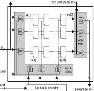
Fig. 2 shows the SCAh-FF and its connectivity. The two major differences are, that the scan-in {si} is now connected to a dedicated scan-out{so} of the preceding register in the scan chain and the register {se[1]} inputs on the same scan depth are connected to the same line-select {ls} signal, which is driven by a “1 out of N ” decoder. SCAh-FF connected to the same line-select signal is considered to be on one line. If { add} is 0, no line is selected. {se[0]} of each SCAh-FF is connected to the global scan enable signal(comparable to the global scan enable signal of shift-scan structures). The output of the address decoder is connected to the {se[1]} pin of the registers on one particular line. Instead of shifting the data through the scan chain, all registers on the same scan depth, enabled by the same line-select signal can be read or written with a single cycle access. Additionally, unselected registers remain in hold mode.
From this structure four different kinds of cycle modes result
“SCA-Structure without HoldMode “demonstrates further to overcome the area disadvantage of the proposed method. The advantages of the SCAh-structure and the lower area overhead of the SCA-structure are combined and presented in Section V, “Gated SCA- Structure”. Sections VI, discusses about the FPGA being used as “XC3s1600e-5fgg484”.The Section VII “Results “compares the static time analysis (STA) of the various modules used in Sections III, IV and The Simulated waveform are also discussed. VIII, “Conclusion”, finish the paper.
III. SCA h-STRUCTURE WITH HOLD MODE A. SCAh-FF
The key element of the single cycle access structure with hold mode (SCAhS) is the signal cycle access register (Flip-Flop, FF) with hold mode (SCAh-FF). It is based on a standard scan register (S-FF) and uses two more 2-to-1 multiplexers. The new SCAh-FF can be seen in Fig. 1.
The SCAh-FF has one more input and one more output com- pared to the standard shift register (S-FF). The inputs clock{clk}, data-in {di}, and scan-in {si} still exists. The scan-enable is now a 2 bit bus {se[0:1]}. An additional scan output pin {so} is added. The reset input and inverse output pins are not shown. The internal logic enables the register to run in one additional
Fig. 1. SCAh-FF based on an S-FF.
TABLE I
TRUTH TABLE OF SCAh-FF
hold mode, whereas the additional output multiplexer can by- pass the register to directly drive the value of {si}. The resulting functionality is best explained by a truth table (see Table I).
In functional mode({se[0:1]}==”00” );the register captures {di} and {so} follows {si} (usually stable). In read mode {s0} has the value of {d0} so that {do} can be read out asynchronously. In the event of the relevant clock edge, the register captures {di}.In hold mode, {so} follows {si}, and the register remains in the state {do}, capturing its own value.When{se [0:1]}:==“11”, the registers captures {si} and {so} changes to the new value of {do} (sync. write/read mode).
The slave latch of a FF is usually connected to the outputdriver of the data-out pin and/or an inverting driver for theinverse-data-out pin.The internal multiplexer for the SCAh-FF (shown in Fig.1) can also be driven by this slave latch output. The fan-out number of the data-out pin (or inverse-data-out pin) refers to the number of input pins which are driven by the SCAh-FF data output drivers.
B. SCAh-FF Connectivity
Fig. 2 shows the SCAh-FF and its connectivity. The two major differences are, that the scan-in {si} is now connected to a dedicated scan-out{so} of the preceding register in the scan chain and the register {se[1]} inputs on the same scan depth are connected to the same line-select {ls} signal, which is driven by a “1 out of N ” decoder. SCAh-FF connected to the same line-select signal is considered to be on one line. If { add} is 0, no line is selected. {se[0]} of each SCAh-FF is connected to the global scan enable signal(comparable to the global scan enable signal of shift-scan structures). The output of the address decoder is connected to the {se[1]} pin of the registers on one particular line. Instead of shifting the data through the scan chain, all registers on the same scan depth, enabled by the same line-select signal can be read or written with a single cycle access. Additionally, unselected registers remain in hold mode.
Fig.2. SCAhS connectivity.
1) When {gse} is low and {add} is 0, the design works in normal functional mode (Table I, line 2). 2) If a specific address is given (asynchronous read), the register values on the selected line are passed to the scan-out bus {s0}. This mode is called asynchronous read mode (Table I, line 3).
3) When { gse } is high and { add } is 0 (no line selected), the design remains in hold mode and no register value changes during an clock edge (Table I, line 4).
4) If a specific address is given at a relevant clock edgeand {gse} is high, the scan-in values {si} are captured by the registers on the selected line (synchronous write) and scan-out { so} is driven by the captured register value (read). This mode is called synchronous write/read (Table I, line 5). The structure is backward compatible to known shift scan operations if {add} is set to 1 at the beginning and automatically incremented after each “shift” cycle. The shift- in data can be written continuously throughout the scan area and the scan-out data can be read at the same time. A capture cycle can also be applied to all registers at the same clock edge (functional mode). The setup time of the SCAh-FF equals the one of the S-FF, because no additional logic is added to the relevant timing path through {di}. The fan-out of {do} is reduced by one because {do} does not drive the {si} of the succeeding register, which is usually the case in SS. The new scan-out {s0} drives the {si} of the succeeding register in the scan chain and has a constant fan-out of 1. The scan chain is decoupled from the functional logic.
C. SCAh-FF Page Organization
The SCAhS enables single cycle read/write accesses to the individual register line. The test structure is now organized in pages to achieve a read/write access at design speed or at a reasonable test speed. The page depth equals the scan chain depth (SD = number of SCAh-FF connected to one chain on one page). Assuming it is 31. Multiplied with the scan width (SW = number of scan chains on one page, for instance 32), the resulting number of SCAh-FF is 992 per page In this rather extreme compact case, the page uses a global1-out-of-31 address line decoder. A page selector {psel} selects the individual page and drives the scan input bus signals andline select {ls} signals (AND-ed) only of this particular page.{psel} can be driven by a register which is set by a dedicated test control logic. If not selected, the page remains inactive to reduce activity. The scan output buses of all pages {so} are bit-wise XOR-ed with the {so} of other pages to generate the global scan-out bus {pso}. If the page is inactive, the XOR-tree passes the value of previous pages unchanged since all {so} bits of an unselected page are “0”.
With the page organization, the relevant timing paths become clear. During a read, the registers are selected by the line-select signal and drive the scan-out bus {so} through a multiplexer chain of the succeeding registers and the page-scan-out bus {pso} through the XOR-tree. During a write, the scan-in bus{si} values are passed through the AND-selector and the multi-plexer chain of the trailing register to the registers of the selected line.
In order to achieve a high test speed, the test implementation can be pipelined. The scan-in bus {si} and the line-select {ls} outputs of the global address-decoder can be registered. Also the XOR-tree can be pipelined with buried register sets. Foreight pages a logic depth of three XOR-cells can be reached. If an optimal test speed cannot be achieved, the scan-depth SD can be reduced (to any number). It is important to notice, that there is no timing path between adjacent registers on the scan chain during test mode ({s0} {si}). Therefore, no hold time problems exist, which are known from shift-scan-test, and no buffers must be inserted for hold time fixes.
synthesis step, but this task can be considered as unproblematic in today’s flows.
The flow for the proposed structure differs only slightly from the one of SS. The standard FF is replaced by a SCAh-FF (in- stead of an S-FF). The global scan-enable signal is identical. The scan connection between registers is now done between the scan-in and the dedicated scan-out of the predecessor (compared to the data-out pin at the standard flow). The address wires of the individual register lines must be routed from the address decoder. The support logic such as the address decoder can be synthesized in a parallel task, but since they have are very regular structure, they can also be elaborated during the test insertion step. A scan reordering during the P&R step can be done without limitations within one page.
The proposed structure can therefore be implemented with acceptable modifications to state-of-the-art P&R tools and is feasible for today’s standard design flows with standard STA tools. No tri-state logic is used.Fig3 depicts the proposed 32 page structure for the “SCA with Hold mode “.
Fig.3. SCAh-page,globalscanenablenotshown.
The proposed structure has the advantage of single cycle write and a single access read of selected register lines.This allows the test method to concentrate on uncovered areas of the combinational logic When data is shifted through the scan chain, the output of the register toggle with a certain probability. This signal change is propagated through the adjacent logic. (Fig 4).In the proposed SCAhS, the scan-in data and the scan-out data toggle asynchronously through a multiplexer chain and are
therefore naturally propagated throughout the complete test cycle. (Fig 5)
Fig.4. S-FF outputs toggle at clock edge.
Fig.5. SCAh-FF chain, propagated scan data toggle, and selected register output toggle at clock edge.
IV.SCA-STRUCTURE WITHOUT HOLD MODE
A. SCA-FF
In order to reduce the area overhead of a SCAhS, a simpler SCA-FF is discussed. It adds only one 2-to-1 MUX to the standard S-FF (see Fig. 6). The truth table is shown in Table VI. It only has one { se } input, which is connected to the individual line-select signal. The pin which is connected to the global en-able signal in the SCAhS is removed, so that the complete global scan enable tree becomes obsolete. The SCA-structure (SCAS) connectivity and page optimization equals the one of the SCAhS (see Figs. 2 and 3) without the global scan enable
TABLE II
TRUTH TABLE OF SCA-FF
se do@clk So mode
0 di si Functional
1 si do Sync.write,asyncread
V. GATED SCA-STRUCTURE
This section discusses the gated SCAS (gSCAS), which has all the benefits of the SCAhS but only has synthesis step, but this task can be considered as
unproblematic in today’s flows.
The flow for the proposed structure differs only slightly from the one of SS. The standard FF is replaced by a SCAh-FF (in- stead of an S-FF). The global scan-enable signal is identical. The scan connection between registers is now done between the scan-in and the dedicated scan-out of the predecessor (compared to the data-out pin at the standard flow). The address wires of the individual register lines must be routed from the address decoder. The support logic such as the address decoder can be synthesized in a parallel task, but since they have are very regular structure, they can also be elaborated during the test insertion step. A scan reordering during the P&R step can be done without limitations within one page.
The proposed structure can therefore be implemented with acceptable modifications to state-of-the-art P&R tools and is feasible for today’s standard design flows with standard STA tools. No tri-state logic is used.Fig3 depicts the proposed 32 page structure for the “SCA with Hold mode “.
Fig.3. SCAh-page,globalscanenablenotshown.
The proposed structure has the advantage of single cycle write and a single access read of selected register lines.This allows the test method to concentrate on uncovered areas of the combinational logic When data is shifted through the scan chain, the output of the register toggle with a certain probability. This signal change is propagated through the adjacent logic. (Fig 4).In the proposed SCAhS, the scan-in data and the scan-out data toggle asynchronously through a multiplexer chain and are
therefore naturally propagated throughout the complete test cycle. (Fig 5)
Fig.4. S-FF outputs toggle at clock edge.
Fig.5. SCAh-FF chain, propagated scan data toggle, and selected register output toggle at clock edge.
IV.SCA-STRUCTURE WITHOUT HOLD MODE
A. SCA-FF
In order to reduce the area overhead of a SCAhS, a simpler SCA-FF is discussed. It adds only one 2-to-1 MUX to the standard S-FF (see Fig. 6). The truth table is shown in Table VI. It only has one { se } input, which is connected to the individual line-select signal. The pin which is connected to the global en-able signal in the SCAhS is removed, so that the complete global scan enable tree becomes obsolete. The SCA-structure (SCAS) connectivity and page optimization equals the one of the SCAhS (see Figs. 2 and 3) without the global scan enable
TABLE II
TRUTH TABLE OF SCA-FF
se do@clk So mode
0 di si Functional
1 si do Sync.write,asyncread
V. GATED SCA-STRUCTURE
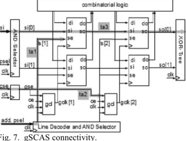
the area overhead of the SCAS. The hold function of the SCAh-FF is missing in the SCA-FF. It is instead built into the gated clock tree of the gSCAS. Fig. 7 shows the connectivity of the gSCA. The scan path reaches from the scan-in AND-selector over the SCA-FF chain (by connecting the scan-out pins of each SCA-FF with the scan-in pins of the succeeding SCA-FF) and is connected with
Fig. 7. gSCAS connectivity.
the input of the XOR-tree. The individual line-select signals{ls} are connected with the { se } input of the SCA-FF in the relevant line. All SCA-FF on a line are clocked by a gated clock element (gcl). The gcl is driven by the clock and the line- select signal. The gated clock element can be enhanced, if a clock en-able signal {ce} generated by combinatorial logic exists. The global scan enable signal is connected with each gcl, which is already the case in SS if gated clock elements are used to propagate the clock during shift.
The gated clock gcl element’s functionality is shown in Table III. If the global scan enable pin {gse} is deselected, the clock is propagated depending on the clock enable signal (functional mode, Table III, line 2 and line 3). In test mode == “1”; the clock is only propagated, if the address line is selected. This allows a hold function if {ls} is not selected (hold mode, Table III, line 4) and a synchronous write if the address line is selected (write mode, Table III, line 5).
TABLE III
TRUTH TABLE OF GATED CLOCK LOGIC
VI.ABOUTXC3s1600e-5fgg484
XC3s1600e-5fgg484 belongs to a SPARTEN-3E FPGA Family
Fig.8.Package OrderingDescriptionOfFPGA
The Spartan-3E family architecture consists offive fundamental programmable functional elements: • Configurable Logic Blocks (CLBs) contain flexible Look-Up Tables (LUTs) that implement logic plus storage elements used as flip-flops or latches. CLBs perform a wide variety of logical functions as well as store data.
• Input/Output Blocks (IOBs) control the flow of data between the I/O pins and the internal logic of the device. Each IOB supports bidirectional data flow plus 3-state operation. It supports a variety of signal standards, including four high- performance differential standards. Double Data-Rate (DDR) registers are included.
• Block RAM provides data storage in the form of 18-Kbit dual-port blocks.
• Multiplier Blocks accept two 18-bit binary numbers as inputs and calculate the product.
• Digital Clock Manager (DCM) Blocks provide self-calibrating, fully digital solutions for distributing, delaying, multiplying, dividing, and phase-shifting clock signals.
VII RESULTS
A .STATIC TIME ANALYSIS
Static timing analysis (STA) is a method of computing the expected timing of a digital circuit without requiring simulation. High-performance integrated circuits have traditionally been characterized by the clock frequency at which they operate. In a synchronous digital system, data is supposed to move in lockstep, advancing one stage on each tick of the clock signal. This is enforced by synchronizing elements such as flip-flops or latches, which copy their input to their output when instructed to do so by the clock. Only two kinds of timing errors are possible in such a system:
the area overhead of the SCAS. The hold function of the SCAh-FF is missing in the SCA-FF. It is instead built into the gated clock tree of the gSCAS. Fig. 7 shows the connectivity of the gSCA. The scan path reaches from the scan-in AND-selector over the SCA-FF chain (by connecting the scan-out pins of each SCA-FF with the scan-in pins of the succeeding SCA-FF) and is connected with
Fig. 7. gSCAS connectivity.
the input of the XOR-tree. The individual line-select signals{ls} are connected with the { se } input of the SCA-FF in the relevant line. All SCA-FF on a line are clocked by a gated clock element (gcl). The gcl is driven by the clock and the line- select signal. The gated clock element can be enhanced, if a clock en-able signal {ce} generated by combinatorial logic exists. The global scan enable signal is connected with each gcl, which is already the case in SS if gated clock elements are used to propagate the clock during shift.
The gated clock gcl element’s functionality is shown in Table III. If the global scan enable pin {gse} is deselected, the clock is propagated depending on the clock enable signal (functional mode, Table III, line 2 and line 3). In test mode == “1”; the clock is only propagated, if the address line is selected. This allows a hold function if {ls} is not selected (hold mode, Table III, line 4) and a synchronous write if the address line is selected (write mode, Table III, line 5).
TABLE III
TRUTH TABLE OF GATED CLOCK LOGIC
VI.ABOUTXC3s1600e-5fgg484
XC3s1600e-5fgg484 belongs to a SPARTEN-3E FPGA Family
Fig.8.Package OrderingDescriptionOfFPGA
The Spartan-3E family architecture consists offive fundamental programmable functional elements: • Configurable Logic Blocks (CLBs) contain flexible Look-Up Tables (LUTs) that implement logic plus storage elements used as flip-flops or latches. CLBs perform a wide variety of logical functions as well as store data.
• Input/Output Blocks (IOBs) control the flow of data between the I/O pins and the internal logic of the device. Each IOB supports bidirectional data flow plus 3-state operation. It supports a variety of signal standards, including four high- performance differential standards. Double Data-Rate (DDR) registers are included.
• Block RAM provides data storage in the form of 18-Kbit dual-port blocks.
• Multiplier Blocks accept two 18-bit binary numbers as inputs and calculate the product.
• Digital Clock Manager (DCM) Blocks provide self-calibrating, fully digital solutions for distributing, delaying, multiplying, dividing, and phase-shifting clock signals.
VII RESULTS
A .STATIC TIME ANALYSIS
• A hold time violation, when an input signal changes too soon after the clock's active transition
• A setup time violation, when a signal arrives too late, and misses the time when it should advance.
a. Timing Constraints
Setup Time ( Best Case Achievable)
Hold Time ( Worst Case
Modules Clks Slack)
SCA_HFF Clk
BUFGP 1.604 ns 1.149 ns SCHFF_CONN Clk
BUFGP 3.315 ns 1.137 ns
gSCAS IBUFCLK 2.619 ns 1.207 ns GCLK1 2.105 ns 1.374 ns
GCLK2 1.740 ns 1.218
Modules Source Destination Delay
Pad Pad
Se<1> S0 5.454
SCA_HFF SI S0 6.01
PI<0> P0 7.688
PI<0> DI<1> 6.235
PI<1> PO 7.983 PI<1> DI<0> 5.503
SCHFF_CONN PI<1> DI<1> 6.53
PI<2> DI<0> 5.64
PI<3> P0 8.433 PI<3> DI<1> 6.98
SI<0> S0<0> 6.558
SI<1> S0<1> 6.569
SE S0 6.637
SCA-FF SI S0 7.047
gSCAS Ipso<0> Sout<0> 5.366
Ipso<1> Sout<1> 5.375
PI<0> P0 6.547 PI<1> P0 7.287 PI<3> P0 7.418
C.DEVICE UTILIZATION SUMMARY
LogicUtilization UsedSCAh_ffAvailable SCAhff_CONNUsed Available UseSCA_ff GSCAS_CONN d Available Used Available Numberof Slice
FlipFlops 1 29,504 6 29,504 1 29,504 9 2
9 , 5 0 4 Numberof4input
LUTs 4 29,504 19 29,504 2 29,504 2
6 29
, 5 0 4 Numberof
occupiedSlices 2 14,752 10 14,752 1 14,752 1
6 14
, 7 5 2 Numberof
Slicescontaining
onlyrelatedlogic 2 2 10 10 1 1 16 16
Numberof Slicescontaining
unrelatedlogic 0 2 0 10 0 1 0 16
Total Numberof 4
inputLUTs 4 29,504 19 29,504 2 29,504 2
7 29
, 5 0 4 Numberusedas
logic - - - 2
6
-Numberusedas
aroute-thru - - - 1
-Numberofbonded
IOBs 8 376 17 376 7 3
7 6
1
7 37
6
IOBFlipFlops - - - - 1 - 1
-Numberof
BUFGMUXs 1 24 1 24 1 2
4 1 24
AverageFanoutof
Non-ClockNets 1.89 - 3.19 - 1.29 - 3.
0 0
-Fig 9(a) SCAh-FF Connectivity FootPrint
VIII. CONCLUSION
A single access structure is discussed.Various architectures with and without hold as well as gated architectures have been explained. A static time analysis (STA) is done on all the architectures and compared .Every architecture is simulated and synthesized in Xilinx. The clock gating technique is applied to gSCAS and the power consumed is 0.203W in XC3s1600e-5fgg484.A 32 page is proposed to be implemented on the FPGA Spartan 3 family.
REFERENCES
[1] Tobias Strauch,” Single Cycle Access Structure for Logic Test”,IEEE Trans. On Very Large Scale Integration System, May 2012
[2] .Rajski, J. Tyszer, M. Kassab, and N. Mukherjee, “Embedded deter- ministic test,” IEEE Trans. Comput.-Aided Des. Integr. Circuits Syst., vol. 23, no. 5, pp. 776–792, May 2004.
[3] D. Czysz, G. Mrugalski, J. Rajski, and J. Tyszer, “Low-power test data application in EDT environment throughdecompression freeze,” IEEE
[4] D. Czysz, M. Kassab, X. Lin, G. Mrugalski, J. Rajski, and J.access scan: Towards low area and routing overhead,” inProc. Asia South PacificTyszer, “Low power scan shift and capture in the EDTenvironment,” in Proc.Des. Autom. Conf., 2008, pp. 565–570
[5] Y. Cho, I. Pomeranz, and S. M. Reddy, “On reducing test application time for scan circuits using limited scan operations and transfer se-quences,” IEEE Trans. Comput.- Aided Des. Integr. Circuits Syst.,vol.24, no. 10, pp. 1594–1605, Oct. 2005.
[6] J. Chen, C. Yand, and K. Lee, “Test pattern generation and clock disabling for simultaneous test time and powerreduction,” IEEE Trans. Computer-Aided Des.Integr. Circuits Syst.,vol.22, no. 3, pp.363–370,Mar. 2003.
[7] S. Wang, “A BIST TPG for low power dissipation and high fault cov- erage,” IEEE Trans. Very Large Scale Integr. (VLSI) Syst., vol. 15, no.7, pp. 777– 789, Jul. 2007.
[8] S. Almukhaizim and O. Sinanoglu, “Dynamic scan chainpartitioning for reducing peak shift power during test,” IEEETrans. Comput.-AidedDes. Integr. Circuits Syst., vol. 28, no. 2, pp. 298–302, Feb. 2009.
[9] A. Al-Yamani, N. Devta-Prasanna, E. Chmelar, M. Grinchuk,and A.Gunda, “Scan test cost and power
reduction through systematicscan re- configuration,” IEEE Trans. Comput.-Aided Des.
Integr. Circuits Syst.,vol. 26, no. 5, pp. 907–917, May 2007.
[10] S. Lin, C. Lee, J. Chen, J. Chen, K. Luo, and W. Wu, “Amultilayer data copy test data compression scheme forreducing shifting-in power for multiple scan design,” IEEE Trans. Very Large Scale Integr. (VLSI)Syst., vol. 15, no. 7, pp. 767– 776, Jul. 2007.
[11] S. Sde-Paz and E. Salomon, “Frequency and power correlationbetween at-speed scan and functional tests,” presented at theInt. Test Conf., Santa Clara, CA, 2008, Paper 13.3.
[12] I. Pomeranz and S. Reddy, “Test compaction for at-speedtesting of scan circuits based on nonscan test sequences and removal of transfer sequences,” IEEE Trans. Comput.-AidedDes. Integr. Circuits Syst., vol. 21, no. 6, pp. 706–714, Jun.2002.
[13] N. Ahmed, M. Tehranipoor, C. Ravikumar, and K. Butler, “Local at-speed scan enable generation for transition fault testing usinglow-cost testers,” IEEE Trans. Comput.-Aided Des. Integr. Circuits Syst., vol. 26, no. 5, pp. 896–906, May 2007.
[14] H. Ando, “Testing VLSI with random access scan,” in Proc.Diag. Pa- pers Compcon 80, 1980, pp. 50–52.
applica- tion time minimization for RAS using basis
optimization of columndecoder,” in Proc. IEEE Int. Symp. Circuits Syst., 2010, pp. 2614–2617. [23] D. Baik and K. Saluja, “Test cost reduction using partitioned grid
random access scan,” in Proc. 19th Int. Conf. VLSI Des.,
2006, pp.1–6
[15] D. Baik and S. Kajthara, “Random access scan: A solution to test power, test data valume and test time,” in Proc. 17th Int. Conf. VLSI
Des., 2004, pp. 883–888.
[16] S. Lin, C. Lee, and J. Chen, “A cocktail approach on randomaccess scan toward low power ad high efficiency test,” in Proc.Conf. Comput.-Aided Des., 2005, pp. 94–99
.
[18] Y. Hu, Y. Han, X. Li, H. Li, and X. Wen, “Compression/scan co-design for reducing test data volume, scan-in power dissipation and test appli-cation time,” in Proc. 11th Pacific Rim Int. Symp. Depend. Comput.,2006, pp. 1–8.
[19] Y. Hu, C. Li, Y. Han, X. Li, W. Wang, H. Li, L. Wang, and X. Wen, “Test data compression based on clustered random access scan,” inProc. 15th Asian Tests Symp., 2006, pp. 231–236.
[20] R. Adiga, G. Arpit, V. Singh, K. Saluja, and A. Singh, “Modified T-flip-flop based scan cell for RAS,” in Proc. 5th IEEE Eur. Test Symp., 2010, pp. 113–118.
[21] A. Mudlapur, V. Agrawal, and A. Singh, “A random access scan ar- chitecture to reduce hardware overhead,” in Proc. Int. Test Conf., 2006,Trans. Comput.-Aided Des. Integr. Circuits Syst., vol. 27, no.7, pp.pp. 350–358.
[22] Y. Hu, X. Fu,X. Fan, and H. Fujiwara, “Localized random1278–1290, Jul. 2008.