Microprocessor Based Signal Processing
Techniques for System Identification and
Adaptive Control of DC-DC Converters
Maher Mohammed Fawzi Saber Algreer
B.Sc., M.Sc.
A thesis submitted for the degree of
Doctor of Philosophy
May, 2012
School of Electrical, Electronic and
Computer Engineering
Newcastle University
United Kingdom
ABSTRACT
Many industrial and consumer devices rely on switch mode power converters (SMPCs) to provide a reliable, well regulated, DC power supply. A poorly performing power supply can potentially compromise the characteristic behaviour, efficiency, and operating range of the device. To ensure accurate regulation of the SMPC, optimal control of the power converter output is required. However, SMPC uncertainties such as component variations and load changes will affect the performance of the controller. To compensate for these time varying problems, there is increasing interest in employing real-time adaptive control techniques in SMPC applications. It is important to note that many adaptive controllers constantly tune and adjust their parameters based upon on-line system identification. In the area of system identification and adaptive control, Recursive Least Square (RLS) method provide promising results in terms of fast convergence rate, small prediction error, accurate parametric estimation, and simple adaptive structure. Despite being popular, RLS methods often have limited application in low cost systems, such as SMPCs, due to the computationally heavy calculations demanding significant hardware resources which, in turn, may require a high specification microprocessor to successfully implement. For this reason, this thesis presents research into lower complexity adaptive signal processing and filtering techniques for on-line system identification and control of SMPCs systems.
The thesis presents the novel application of a Dichotomous Coordinate Descent (DCD) algorithm for the system identification of a dc-dc buck converter. Two unique applications of the DCD algorithm are proposed; system identification and self-compensation of a dc-dc SMPC. Firstly, specific attention is given to the parameter estimation of dc-dc buck SMPC. It is computationally efficient, and uses an infinite
impulse response (IIR) adaptive filter as a plant model. Importantly, the proposed method is able to identify the parameters quickly and accurately; thus offering an efficient hardware solution which is well suited to real-time applications. Secondly, new alternative adaptive schemes that do not depend entirely on estimating the plant parameters is embedded with DCD algorithm. The proposed technique is based on a simple adaptive filter method and uses a one-tap finite impulse response (FIR) prediction error filter (PEF). Experimental and simulation results clearly show the DCD technique can be optimised to achieve comparable performance to classic RLS algorithms. However, it is computationally superior; thus making it an ideal candidate technique for low cost microprocessor based applications.
DEDICATION
ACKNOWLEDGMENTS
I would like to acknowledge everyone for those who made this work possible to complete. First and foremost, I would like to thank God that gives me the patience to complete this work, praise to God.
I would also like to express my deep sincere gratitude towards all my supervisors Dr. Matthew Armstrong, Dr. Damian Giaouris, and Dr. Petros Missailidis for their support, patient guidance and encouragement during my doctoral research. The successful achievement of this work would not be complete without their support. I would like to extend my thanks to Dr. Matthew Armstrong for his amicable nature that he has provided for positive free stress collaboration and for sharing his expertise in practical design. Honestly, he has an exemplary role that always presented kinds words for encouragement.
My acknowledgments also go to my friends and colleagues at PEDM Lab, for their collaboration. My thanks also go to Bassim Jassim for sharing his knowledge on power electronics. In addition, I would like to thank the academic and technicians staff in EECE for their cooperation. My thank towards the head of school Prof. Bayan Sharif for his collaboration during my life in Newcastle city. I thank Mrs Gillian Webber and Deborah Alexander for help in all the administrative work.
I am also grateful indebted to Dr. Yuriy Zakharov of the University of York, for his valuable comments and advice received from him on the DCD algorithm.
I would like to gratefully appreciate the Ministry of Higher Education, from my home country IRAQ, for the financial support during this research, without their sponsorship, I could not complete this work.
Finally, my deepest appreciation to my father and mother, for their love and continues support they provide me through my entire life. I am always imagining my parent happiness when I will be successes in PhD to encourage myself progressing more. I owe all that I have. I would like to warmly thank all my brothers, my lovely sister Moroj and my sons Mohib and Majd, they give me the power to complete this work and give me endless morale support. Last but most important, to say thanks to my wife ISRAA, you always encourage me, given me the strength and enthusiasm to complete this research, she always face the same tension and frustration that I had during my work. This project would not be complete without her understanding and love.
TABLE OF CONTENTS
ABSTRACT ... II DEDICATION ... IV ACKNOWLEDGMENTS ... V LIST OF FIGURES ... XII LIST OF TABLES ... XIX LIST OF ACRONYMS ... XX LIST OF SYMBOL ... XXII
Chapter 1 INTRODUCTION AND SCOPE OF THE THESIS ... 1
1.1 Introduction ... 1
1.2 Scope and Contribution of the Thesis ... 4
1.3 Publications Arising from this Research ... 6
1.4 Layout of the Thesis ... 7
1.5 Notations ... 8
Chapter 2 DC-DC SWITCH MODE POWER CONVERTERS MODELLING AND CONTROL ... 9
2.2 DC-DC Circuit Topologies and Operation ... 9
2.2.1 DC-DC Buck Converter Principle of Operation ... 11
2.3 DC-DC Buck Converter Modelling ... 11
2.4 Model Simulation ... 14
2.5 Buck State Space Average Model ... 15
2.6 Discrete Time Modelling of Buck SMPC ... 17
2.7 Digital Control Architecture for PWM DC-DC Power Converters ... 18
2.7.1 Digital Voltage Mode Control ... 20
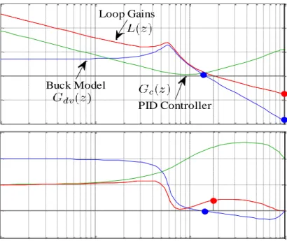
2.8 Digital Proportional-Integral-Derivative Control ... 22
2.8.1 Digital Control for Buck SMPC Based on PID Pole-Zero Cancellation ... 25
2.8.2 Pole Placement PID Controller for DC-DC Buck SMPC ... 31
2.9 Chapter Summary ... 37
Chapter 3 SYSTEM IDENTIFICATION, ADAPTIVE CONTROL AND ADAPTIVE FILTER PRINCIPLES -A LITERATURE REVIEW ... 38
3.1 Introduction ... 38
3.2 Introduction to System Identification ... 38
3.3 Parametric and Non-Parametric Identification ... 40
3.4 Model Structures for Parametric Identification ... 43
3.5 Parametric Identification Process ... 46
3.6 Adaptive Control and Adaptive Filter Applications ... 47
3.7 Adaptive Control Structures ... 48
3.9 Literature Review on System Identification and Adaptive Control for DC-DC
Converters ... 53
3.9.1 Non-Parametric System Identification Techniques and Adaptive Control for SMPC ... 53
3.9.2 Parametric Estimation Techniques and Adaptive Control for SMPC ... 55
3.9.3 Independent Adaptive Control Technique for SMPC ... 60
3.10 Chapter Summary ... 62
Chapter 4 SYSTEM IDENTIFICATION OF DC-DC CONVERTER USING A RECURSIVE DCD-IIR ADAPTIVE FILTER ... 63
4.1 Introduction ... 63
4.2 System Identification of DC-DC Converter Using Adaptive IIR DCD-RLS Algorithm ... 65
4.3 Adaptive System Identification ... 67
4.4 Least Square Parameters Estimation ... 68
4.5 Conventional RLS Estimation ... 70
4.6 Normal Equations Solution Based On Iterative RLS Approach ... 72
4.6.1 Exponentially Weighted RLS Algorithm (ERLS) ... 74
4.7 Coordinate Descent and Dichotomous Coordinate Descent Algorithms ... 76
4.7.1 Dichotomous Coordinate Descent Algorithm ... 80
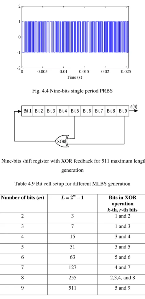
4.8 Pseudo-Random Binary Sequence and Persistence Excitation ... 82
4.9 Discrete Time Modelling of DC-DC Converter and Adaptive IIR Filter ... 86
4.9.1 Equation Error IIR Adaptive Filter ... 88
4.11 Model Example and Simulation Results ... 92
4.12 Adaptive Forgetting Strategy ... 101
4.12.1 Fuzzy RLS Adaptive Method for Variable Forgetting Factor ... 101
4.13 Simulation Test ... 106
4.14 Chapter Summary ... 110
Chapter 5 ADAPTIVE CONTROL OF A DC-DC SWITCH MODE POWER CONVERTER USING A RECURSIVE FIR PREDICTOR ... 112
5.1 Introduction ... 112
5.2 Self-Compensation of a DC-DC Converter Based on Predictive FIR ... 113
5.3 Auto-Regressive / Process Generation, Identification... 114
5.3.1 Relationship between Forward Prediction Error Filter and AR Identifier116 5.3.2 One-Tap Linear FIR Predictor for PD Compensation ... 120
5.4 Least Mean Square Algorithm... 121
5.5 Simulation Results ... 124
5.5.1 Reference Voltage Feed-Forward Adaptive Controller ... 125
5.5.2 Voltage Control Using Adaptive PD+I Controller ... 128
5.6 Robustness and Stability Analysis for the Proposed Adaptive PD+I Controller ... 134
5.7 Chapter Summary ... 138
Chapter 6 MICROPROCESSOR APPLICATION BASED SYNCHRONOUS DC-DC SWITCH MODE POWER CONVERTER-EXPERIMENTAL RESULTS ... 139
6.2 Microprocessor Control Platform ... 139
6.2.1 Microprocessor Code Development ... 141
6.3 System Hardware Description and Microprocessor Setup ... 142
6.4 System Identification Using DCD-RLS / Experimental Validation... 148
6.5 Realisation of the Converter Model ... 155
6.6 Adaptive Controller / Experimental Validation ... 157
6.7 Complexity Reduction ... 162
6.8 Chapter Summary ... 165
Chapter 7 CONCLUSION AND FUTURE WORK ... 166
7.1 Conclusion ... 166
7.2 Future Work ... 169
APPENDIX A ... 172
DERIVATION OF RLS ALGORITHM BASED ON MATRIX INVERSION LEMMA ... 172
APPENDIX B ... 175
SCHEMATIC CIRCUIT OF THE SYNCHRONOUS BUCK CONVERTER 175 APPENDIX C ... 178
SIMULINK MODEL OF THE PROPOSED STRUCTURES ... 178
LIST
OF
FIGURES
Fig. 1.1 Dual core microprocessor and digital control architecture for SMPCs ... 3
Fig. 2.1 Most common dc-dc converter topologies, a: buck converter, b: boost converter, c: buck-boost converter ... 10
Fig. 2.2 Buck converter circuit configuration, a: On state interval, b: Off state interval... 13
Fig. 2.3 Open loop steady state output voltage ... 14
Fig. 2.4 Open loop steady state inductor current ... 15
Fig. 2.5 Digital voltage mode control architecture of DC-DC SMPC...20
Fig. 2.6 Two-poles / Two-zeros IIR digital controller ... 22
Fig. 2.7 Digital PID compensator ... 23
Fig. 2.8 Frequency response of the compensated and uncompensated dc-dc buck SMPC ... 28
Fig. 2.9 Power stage root locus ... 28
Fig. 2.10 PID compensator root locus ... 29
Fig. 2.11 Total loop gains root locus ... 29
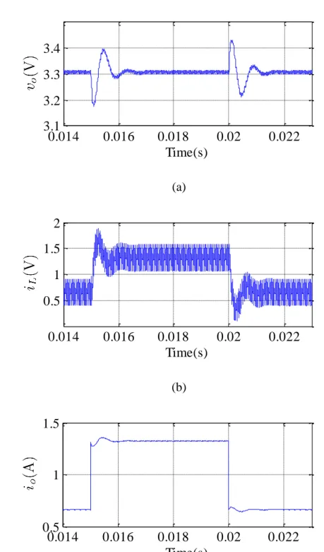
Fig. 2.12 Transient response of the PID controller, a: output voltage, b: inductor current, c: load current. Load current change between 0.66 A and 1.32 A every 5 ms ... 30
Fig. 2.14 Frequency response of the compensated and uncompensated dc-dc buck
SMPC ... 34
Fig. 2.15 Transient response of the pole-placement PID controller, a: output voltage, b: inductor current, c: load current. Load current change between 0.66 A and 1.32 A every 5 ms ... 35
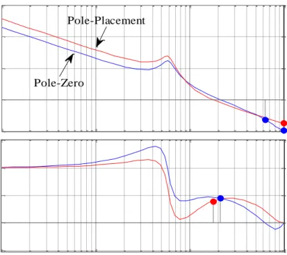
Fig. 2.16 Loop-gain comparison between pole-placement and pole-zero PID controllers ... 36
Fig. 2.17 Comparison of transient response results between pole-placement and pole-zero PID controllers. Repetitive load current change between 0.66 A and 1.32 A every 5 ms ... 36
Fig. 3.1 General block diagram of parametric identification ... 39
Fig. 3.2 General linear model transfer function ... 41
Fig. 3.3 Parametric identification model structures ... 44
Fig. 3.4 Parametric identification flowchart ... 46
Fig. 3.5 Adaptive model reference structure ... 48
Fig. 3.6 Self-tuning controller block-diagram ... 49
Fig. 3.7 An adaptive filter structure ... 50
Fig. 3.8 Adaptive Filter structures, a: system identification, b: signal prediction, c: inverse modelling, d: noise cancellation ... 52
Fig. 4.1 The proposed closed loop adaptive IIR identification method using DCD-RLS algorithm ... 65
Fig. 4.2 Adaptive system identification block diagram ... 67
Fig. 4.3 Closed loop operation of conventional RLS algorithm based matrix inversion lemma ... 71
Fig. 4.5 Nine-bits shift register with XOR feedback for 511 maximum length
PRBS generation ... 84
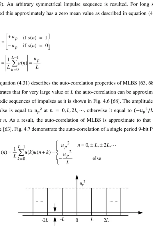
Fig. 4.6 Ideal auto-correlation of an infinite period of PRBS ... 85
Fig. 4.7 Single period 9-bit auto-correlation of PRBS ... 86
Fig. 4.8 System identification based on adaptive IIR filter using output error block diagram ... 88
Fig. 4.9 System identification based on adaptive IIR filter using equation error block diagram ... 90
Fig. 4.10 The procedure of system identification ... 93
Fig. 4.11 Identification sequence, a: output voltage during ID, b: voltage model parameters ID, c: voltage error prediction, d. ID enable signal ... 95
Fig. 4.12 Tap-weights estimation for IIR filter using DCD-RLS and classical RLS methods; compared with calculated model ... 97
Fig. 4.13 Prediction error signals, a: classical RLS, b: DCD-RLS ... 97
Fig. 4.14 Parameters estimation error, a: classical RLS, b: DCD-RLS ... 98
Fig. 4.15 Tap-weights estimation DCD-RLS at Nu = 4 and classical RLS ... 99
Fig. 4.16 Tap-weights estimation DCD-RLS and CD algorithms ... 99
Fig. 4.17 Frequency responses for control-to-output transfer of function; estimated and calculated model ... 100
Fig. 4.18 The proposed system identification structure for a dc-dc converter based on RLS fuzzy AFF ... 102
Fig. 4.19 General block diagram of the fuzzy logic system ... 103
Fig. 4.20 Fuzzy logic input and output membership functions, a: ep2,b:Δep2 , c: λ ... 105
Fig. 4.21 Parameters estimation of control-to-output voltage transfer of a dc-dc converter at load changes from 5-to-1ΩusingDCD-RLS algorithm at a: λ = 0.7, b: λ
= 0.99, c: fuzzy AFF ... 108
Fig. 4.22 Prediction error signal during initial start-up and at load change ... 109
Fig. 4.23 Forgetting factor at initial start-up and at load change ... 109
Fig. 5.1 Adaptive PD+I controller using one tap DCD-RLS PEF ... 113
Fig. 5.2 Reconstruction of white noise ... 114
Fig. 5.3 AR process generator ... 115
Fig. 5.4 AR process identifier ... 116
Fig. 5.5 One step ahead forward predictor ... 117
Fig. 5.6 Forward prediction error filter ... 118
Fig. 5.7 Prediction error filter ... 118
Fig. 5.8 AR analyser, a: matched Inverse MA filter, b: one tap adaptive PEF, c: two tap adaptive PEF filter. The dotted line is the estimated output and the solid line is the actual input ... 119
Fig. 5.9 Closed loop LMS system block diagram ... 124
Fig. 5.10 Reference voltage feed-forward: Comparison of transient response between LMS and DCD-RLS. Repetitive load change between 0.66 A and 1.32 A every 5 ms ... 125
Fig. 5.11 Zoomed adaptation of gain (Kd) and tap-weight (w1) in the two stage adaptive linear predictor for different step-size values ... 127
Fig. 5.12 Transient response of the proposed adaptive controller, a: output voltage, b: inductor current, c: load current change between 0.66A and 1.32 A every 5 ms . 129
Fig. 5.13 Error signal behaviour during adaptation process, a: loop error (eL), b: prediction error (ep1). Load current change between 0.66 A and 1.32 A every 5 ms 130
Fig. 5.14 Transient response of the proposed adaptive PD+I controller using
DCD-RLS or LMS. Load current change between 0.66 A and 1.32 A every 5 ms... 131
Fig. 5.15 Transient response of the proposed adaptive controller during load current change between 0.66 A and 1.32 A every 5 ms, a: output capacitance C = 150 μFandL =220μH,b:C = 660μFandL =220μH,c:outputinductorL =100μH and C =330μF ... 133
Fig. 5.16 Comparison of transient response results between the proposed adaptive PD+I using DCD-RLS and pole-zero PID control. Repetitive load current change between 0.66 A and 1.32 A every 5 ms ... 134
Fig. 5.17 Frequency response of the PD + I compensator and the compensated / uncompensated open loop gains... 135
Fig. 5.18 Closed loop scheme of voltage mode control for SMPC ... 136
Fig. 5.19 Sensitivity functions of the PD+I controller ... 137
Fig. 5.20 Margins on Nyquist plot ... 137
Fig. 6.1 TMS320F28335 eZdsp Architecture [129] ... 140
Fig. 6.2 Hardware platform setup ... 142
Fig. 6.3 Block diagram of the synchronous dc-dc buck converter based on microprocessor ... 143
Fig. 6.4 a: TMS320F28335™ DSP platform, b: the synchronous dc-dc buck converter circuit ... 145
Fig. 6.5 PWM waveforms in open loop circuit test, a: duty ratio 50 % , b: duty ratio 33 % ... 147
Fig. 6.6 Leading DCD-RLS algorithm flowchart ... 148
Fig. 6.7 Experimental output voltage waveform when identification enabled. (ac coupled) ... 149
Fig. 6.8 Experimental output voltage and persistence excitation signal (duty signal +∆PRBS) results during ID, based on sampled data collected from DSP ... 151
Fig. 6.9 Experimental tap-weights estimation for IIR filter with DCD-RLS and classical RLS methods; compared with the calculated model ... 152
Fig. 6.10 Experimental prediction error results, a: conventional RLS, b: DCD-RLS ... 152 Fig. 6.11 Experimental parameters estimation error, a: classical RLS, b: DCD-RLS ... 153 Fig. 6.12 Experimental learning curves comparison results of conventional RLS against DCD-RLS at different iteration values ... 154
Fig. 6.13 Experimental sampled data collected from DSP, a: output voltage, b: controlsignal(dutysignal+∆PRBS) ... 155
Fig. 6.14 Model errors comparison between third/second order output error and equation error model ... 156
Fig. 6.15 Transient response of PID controller with abrupt load change between 0.66 A and 1.32 A. (a) 4 ms/div: showing two transient changes. (b) 400 µs/div: “zoom-in”onsecondtransient ... 159
Fig. 6.16 Transient response of adaptive PD+I DCD-RLS controller with abrupt load change between 0.66 A and 1.32 A. (a) 4 ms/div: showing two transient changes. (b)400µs/div:“zoom-in”onsecondtransient ... 160
Fig. 6.17 Transient response of adaptive PD+I LMS controller with abrupt load change between 0.66 A and 1.32 A. (a) 4 ms/div: showing two transient changes. (b) 400µs/div:“zoom-in”onsecondtransient ... 161
Fig. 6.18 Load transient response at significant change in load current, with two stage DCD-DCD adaptive controller and hybrid DCD-LMS adaptive controller .... 163
Fig. 6.19 Transient response of hybrid DCD-RLS:LMS (µ = 1) adaptive controller with abrupt load change between 0.66 A and 1.32 A. (a) 4 ms/div: showing two transientchanges.(b)400µs/div:“zoom-in”onsecondtransient ... 164
LIST
OF
TABLES
Table 4.1Conventional RLS algorithm based matrix inversion lemma ... 71
Table 4.2 Iteratively solving for auxiliary equations ... 74
Table 4.3 ERLS algorithm using auxiliary equations ... 76
Table 4.4 Exact line search algorithm description ... 77
Table 4.5 Cyclic CD algorithm description ... 79
Table 4.6 Leading CD algorithm description ... 79
Table 4.7 Cyclic DCD algorithm description ... 80
Table 4.8 Leading DCD algorithm description ... 82
Table 4.9 Bit cell setup for different MLBS generation ... 84
Table 4.10 Discrete time control-to-output transfer function identification ... 100
Table 4.11 The rule base for the forgetting factor (λ) ... 106
Table 5.1 LMS algorithm operation ... 124
LIST
OF
ACRONYMS
AC Alternating Current
ADC Analogue -to-Digital Converter AR Auto-Regressive
ARMA Auto Regressive Moving Average Model CCM Continuous Conduction Mode
CCS Code Composer Studio CD Coordinate Descent CPU Central Processing Unit
DAC Digital-to-Analogue Converter DC Direct Current
DCD Dichotomous Coordinate Descent DCM Discontinuous Conduction Mode DPWM Digital Pulse Width Modulation DSP Digital Signal Processor
ERLS ExponentiallyWeighted Recursive Least Square FFT Fast Fourier Transform
FL Fuzzy logic
FPGA Field Programmable Gate Array IC Integrated Circuit
IDE Integrated Development Environment IIR Infinite Impulse Response
LCO Limit Cycle Oscillation LMS Least Mean Square LS Least Square
LTI Linear Time Invariant MA Moving Average
MLBS Maximum Length Pseudo Binary Sequence
MOSFET Metal–Oxide–Semiconductor Field-Effect Transistor MSE Mean Square Error
PD Proportional-Derivative PEF Prediction Error Filter PI Proportional-Integral
PID Proportional-Integral-Derivative PRBS Pseudo Random Binary Sequence RLS Recursive Least Square
SI System Identification
SMPC Switch Mode Power Converter ZOH Zero-Order-Hold
LIST
OF
SYMBOL
µ Step size C Capacitor d(n) Control signal ep Prediction error fo Corner frequency fs Sampling frequency iL Inductor current io Load current KD Derivative gain KI Integral gain KP Proportional gain L Inductor Mp Maximum overshoot Q Quality Factor tr Time rise Tsw Switching timevC Capacitor voltage
Vin Input voltage
vL Inductor voltage
vo Output voltage
Vref Reference voltage ŵ Estimated filter weight
ŷ Estimated output ΔPRBS PRBS amplitude θ Parameters vector
λ Forgetting factor φ Regression vector
Chapter 1
INTRODUCTION
AND
SCOPE
OF
THE
THESIS
1.1Introduction
Many classical control schemes for switch mode power converters (SMPCs) suffer from inaccuracies in the design of the controller. This may be due to poor knowledge of the load characteristics, or unexpected external disturbances in the system. In addition, SMPC uncertainties such as component tolerances, unpredictable load changes, changes in ambient conditions, and ageing effects, all affect the performance of the controller over time [1, 2]. Consequently, greater consideration should be given to the design of the controller to accommodate these uncertainties in the system. Therefore, an intermediate process is required to explicitly determine the parameters of the power converter and to estimate the dynamic characteristics of the SMPC. This process can be achieved by system identification algorithms. Also, in SMPC applications, often a classical Proportional-Integral-Derivative (PID) controller is employed using fixed controller gains. In such systems, the fixed control loop is unable to consider parameter changes that may occur during the normal operation of the plant. Ultimately, this limits the stability margins, robustness, and dynamic performance of the control system [3].
For this reason, more advanced auto-tuning and adaptive digital controllers are now playing an increasingly important role in SMPC systems. With the advent of developments in digital control techniques, intelligent and advanced control algorithms can now readily be incorporated into the digital based systems to significantly improve the overall dynamic performance of the process. On-line
identification, system monitoring, adaptive and self-tuning controllers are some of the most attractive features of digital control systems. These intelligent algorithms, which are well suited to SMPC applications, allow more optimised control designs to be realised [2, 4] and can rapidly adjust controller settings in response to system parameter variation. Clearly, an accurate model is required (transfer function, state space), and therefore excellent estimation of plant parameters is essential. Here, the controller tuning is based upon on-line system identification techniques, and therefore a discrete time transfer function of the SMPCs is necessary for control design [5, 6]. This is particularly true in most adaptive and self-tuning controllers which require system identification to update the control parameters. The fundamental principle of system identification and parameter estimation is to evaluate the parameters within a transfer function which has an analogous arrangement to the actual plant to be controlled. However, system identification and adaptive controllers are not fully exploited in low cost, low power SMPCs due to the heavy computational burden they place upon the microprocessor platform. Complex algorithms often require higher performance hardware to implement and this is usually cost prohibitive in applications such as SMPCs [7]. Therefore, there is a requirement to further research and develop cost effective, computationally light identification and adaptation methods which offer accurate estimation performance.
Recent developments in digital hardware; including microprocessors, microcontrollers, digital signal processors (DSP) and field programmable gate arrays (FPGA), provide the ability to design and implement a complex system at higher sampling rate, such as adaptive and self-tuning controllers. However, the execution time of adaptive algorithms is dependent upon several factors: processor architectures, memory, data/address bus widths, clock rate, etc.
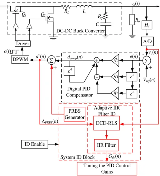
Fortunately, the industrial electronics companies have been attempting to release adaptive and self-tuning controllers in SMPC applications. The scheme of these controllers is based upon real time identification and system monitoring of SMPCs, using new microprocessor architecture; including multiprocessor cores (Fig. 1.1). As shown in Fig. 1.1, the digitally controlled block-diagram of SMPCs is classified as a mixed signal system. In this structure two kinds of signals are used: analogue/digital
or discrete signal. The analogue system consists of dc-dc power stage circuit, sensing/signal conditioning circuit, and gate drive circuit. The digital system consists of digital compensator, a digital-pulse-width-modulation (DPWM) circuit and an analogue-to-digital converter (ADC) that provides an interface between the digital and analogue domains.
Analogue System Signal Conditioning and Sensing vo(n) Vref (n) e(n) d (n) DPWM DC-DC Converter + A/D Digital Control c (t) vsensing(t) Microprocessor unit Gate Drive g (t) − vo(t)
Self-Tuning and Adaptive Controller/ System Identification Core 2 Microprocessor Core 1 Microprocessor Non-Linear Compensation Control Unit System Bus
Fig. 1.1 Dual core microprocessor and digital control architecture for SMPCs The new configuration of Power Electronics Management (PEM) will increase the performance of the microprocessor without increasing the power consumption. Here, the tasks are divided between the two processor cores. The first microprocessor core is designed for simple control regulation such as a conventional digital PID control. The second microprocessor core provides advanced control implementation, for instance adaptive and system identification algorithm. In some PEM units, non-linear control techniques have also been introduced in the second microprocessor core to further improve the transient characteristics of the system. As illustrative examples, “POWERVATION®” creates a dual core PEM-IC (PV3002). This IC is capable of
(output capacitor/inductor) based on cycle-by-cycle output voltage monitoring. The PV3002 includes several analogue circuits, DSPs, and a reduced instruction set computing (RISC) microprocessor [8, 9].“INTERSIL Zilker Labs”designedadigital
adaptive controller IC, namely the ZL6100. This processor can compensate the feedback loop automatically to produce optimal controller performance during output load changes. A non-linear controller utilises this architecture to further improve the dynamic response in the event of abrupt load change [10]. In another example from
TEXAS INSTRUMENTS (TI), the attractive features of system identification have been used for the purpose of monitoring the performance of SMPCs, and to update the feedback control loop. In this device (UCD9240) non-linear gains have been augmented to further improve the dynamic behaviour of the system [11, 12].
1.2Scope and Contribution of the Thesis
Recent advances in microprocessor technology and continual price improvement now allows for more advanced signal processing algorithms to be implemented in many industrial and commercial products, cost and complexity are clearly a major concern. For this reason, the aim of this thesis is to research new practical solutions for system identification and adaptive control that can easily be developed in low complexity systems, whilst maintaining the performance of conventional algorithms. Particular attention is given to parametric estimation and self-compensator design of switch mode dc-dc power converters. In this thesis, the work is applied to a small synchronous dc-dc buck converter. However, the proposed techniques are transferable to other applications.
In order to quickly and accurately identify the system dynamics of a SMPC, a new adaptive method known as Dichotomous Coordinate Descent-Recursive-Least-Square (DCD-RLS) algorithm is proposed. An equation error IIR adaptive filter scheme is developed along with the DCD-RLS algorithm for system modelling of dc-dc SMPC. The design and implementation of the proposed DCD-RLS technique is presented in detail, and results are compared and verified against classical techniques (RLS). A major conclusion from the work is that the DCD-RLS can achieve similar estimation performance to the classic RLS technique, but with a lighter computational burden on the microprocessor platform. The proposed scheme has successfully been presented
by the author in [13]. In addition, an enhancement on the scheme is suggested by employing a variable forgetting factor based fuzzy logic algorithm for the identification of the SMPC parameters. The concept of this scheme is presented in the thesis and the advantages it delivers are discussed. The simulation results for the proposed adaptive forgetting factor with fuzzy logic scheme has been published by the author in [14].
System identification is a first step to developing adaptive and self-tuning controllers. Therefore, the computation complexity of these structures is typically very high. Furthermore, in order to achieve a good quality, dynamic closed loop control system, the unknown parameters of the plant should be estimated quickly and accurately. With these issues in mind; this thesis presents a new alternative adaptive scheme that does not depend entirely on estimating the plant parameters. This scheme is based on adaptive signal processing techniques which are suitable for both prediction/identification and controller adaptation. Importantly, and explained in detail in this thesis, the method the use of an adaptive prediction error filter (PEF) as a main control in the feedback loop. A two stage/one-tap FIR adaptive PEF is placed in parallel with a conventional integral controller to produce an adaptive Proportional-Derivative + Integral (PD+I) controller. The DCD-RLS algorithm is incorporated into the PD+I controller for real time estimation of the PEF tap-weights and for reducing the computational complexity of the classical RLS algorithms for efficient hardware implementation. Simulation and experiments results of the proposed scheme have been published by the author in [15, 16]. The mathematical analysis and concept of using an adaptive PEF for adaptive control, and the relationship between an adaptive PEF and a Proportional-Derivative (PD) controller, are clearly described by the author in the thesis and have been published in [17]. In summary, the main objectives and contributions of this research are:
To propose a novel method, based on the DCD algorithm, for on-line system identification of dc-dc converters.
Application of the DCD-RLS algorithm to reduce computation complexity compared to classical methods (RLS).
To develop an equation error IIR adaptive filter for system modelling of dc-dc converters based upon the DCD-RLS algorithm.
To apply an adaptive forgetting factor strategy to track the time varying parameters of SMPCs using a fuzzy logic approach.
To develop a new adaptive controller for SMPCs based upon an FIR prediction error filter using DCD-RLS and LMS adaptive algorithms.
To experimentally assess the performance of the proposed adaptive DCD-RLS algorithm using a Texas Instruments TMS320F28335 DSP platform and synchronous dc-dc buck converter.
1.3Publications Arising from this Research
The research in this thesis has resulted in number of journals and international conference publications. These articles are listed below:
1- M. Algreer, M. Armstrong, and D. Giaouris, “Active On-Line System Identification of Switch Mode DC-DC Power Converter Based on Efficient Recursive DCD-IIR Adaptive Filter”, IEEE Transactions on Power Electronics, vol.27, pp.4425-4435, Nov. 2012.
2- M. Algreer, M. Armstrong, and D. Giaouris, “Adaptive PD+I Control of a Switch Mode DC-DC Power Converter Using a Recursive FIR Predictor”,
IEEE Transactions on Industry Applications, vol.47, pp.2135-2144,Oct. 2011. 3- M. Algreer,M.Armstrong,andD.Giaouris,“PredictivePIDControllerfor
DC-DC Converters Using an Adaptive Prediction Error Filter,” inProc. IET International Conf. on Power Electron., Machines and Drives, PEMD 2012, vol. 2012, Bristol, United Kingdom.
4- M. Algreer,M.Armstrong,andD.Giaouris,“AdaptiveControlofaSwitch Mode DC-DC Power Converter Using a Recursive FIR Predictor,” inProc.
IET International Conf. on Power Electron., Machines and Drives, PEMD
5- M. Algreer, M. Armstrong, and D. Giaouris, "System Identification of PWM DC-DC Converters during Abrupt Load Changes," in Proc. IEEE Industrial Electron. Conf., IECON'09, 2009, pp. 1788 – 1793, Porto, Portugal.
1.4Layout of the Thesis
The thesis is organised into 7 chapters as follow:
Chapter 2 presents the modelling and control of dc-dc power converters. This includes the common circuit topologies of dc-dc converters with more emphasis on operation and circuit configuration of buck dc-dc switch mode power converters. It also provides details on derivation of the continuous state space model, followed by details on average and discrete models of buck dc-dc converter. A digital voltage mode control structure is introduced in this chapter; sub-circuit blocks are also explained. In the digital control section, two techniques of digital compensator are discussed including the pole-zero cancellation method and pole-placement approach. The modelling and control in this chapter will be used to evaluate the proposed algorithms.
Chapter 3 provides details on the principles and techniques used in system identification. Different common models of parametric estimation techniques are also demonstrated. In addition, it outlines basic information on adaptive control and adaptive filter techniques. Recent publications on system identification/adaptive control techniques for dc-dc SMPCs are also reviewed in this chapter.
Chapter 4 presents details on the derivation of the classical LS and RLS algorithms. In addition, it briefly explains the system identification paradigm based adaptive filter technique. The proposed on-line system identification scheme for SMPC is also described in this chapter. This is followed by in-depth analyses and derivation of the new DCD-RLS adaptive algorithm along with equation error IIR adaptive filter structure. Each sub block in the on-line system identification structure is explained. Furthermore, Chapter 4 explores a new adaptive forgetting factor based fuzzy logic system to detect and estimate the fast change in the system via sudden change in prediction error signal. The new identification schemes in this chapter are comprehensively tested and validate through simulations.
Chapter 5 presents the proposed adaptive controller. The first part of this chapter provides details on the principle of how an adaptive PEF filter can be employed as a central controller in the feedback loop of a closed loop system. Following this, an overview of auto-regressive and moving average filters is presented along with the derivation of the Least-Mean-Square (LMS) adaptive algorithm. In addition, Chapter 5 demonstrates the effectiveness of the DCD-RLS adaptive algorithm to improve the dynamics performance of the proposed adaptive scheme. Robustness and stability analysis of the proposed controller is discussed. Extensive simulation results that compare the proposed adaptive control based upon DCD-RLS with classical LMS are provided in this chapter.
Chapter 6 focuses on the experimental validation of the developed adaptive algorithms using a high speed microprocessor board. It provides an overview on the architecture of the selected digital signal processor platform. In addition, this chapter explains the practical circuit diagram of the constructed dc-dc buck converter and the experimental setup. Importantly, Chapter 6 concentrates on practical evaluation of the proposed system identification algorithm and adaptive controller structure. It also provides a comparison between the obtained experimental results of the proposed scheme using the DCD-RLS algorithm and the classical RLS/LMS algorithms, as well as with the conventional digital PID controller.
Finally, Chapter 7 presents the conclusion drawn for this thesis and it summarises possible suggestions for future work.
1.5Notations
In this thesis the matrices and vectors are represented by bold upper case and bold lower case characters respectively. As an illustrative example, R and r.The elements of the matrix and vector are denoted as Ri,i and ri. The i-th column of R is denoted as R(i). Finally, variable n is used as a time index, for instance β(n) is the vector β at time instant n.
Chapter 2
DC-DC
SWITCH
MODE
POWER
CONVERTERS
MODELLING
AND
CONTROL
2.1Introduction
DC-DC SMPCs are extensively used in a wide range of electrical and electronic systems, with varying power levels (typically mW-MW applications). Some illustrative examples are power supplies in personal/laptop computers, telecommunications devices, motor drives, and aerospace systems. These applications require SMPCs with a high performance voltage regulation during static and dynamic operations, high efficiency, low cost, small size/lightweight, and reliability [18-20]. The main role of dc-dc converters is to convert the unregulated DC input voltage into a different regulated level of DC output voltage. In general, a dc-dc converter can be described as an analogue power processing device that contains a number of passive components combined with semiconductor devices (diodes and electronics switches) to produce a regulated DC output voltage that has a different magnitude from the DC input voltage. Some examples refer to the power supply of the microprocessor and other integrated circuits that require a low regulated DC voltage between 3.3 V and 5 V. This voltage is resultant from the reduction of the high DC voltage generated from an AC-to-DC power rectifier [18].
2.2DC-DC Circuit Topologies and Operation
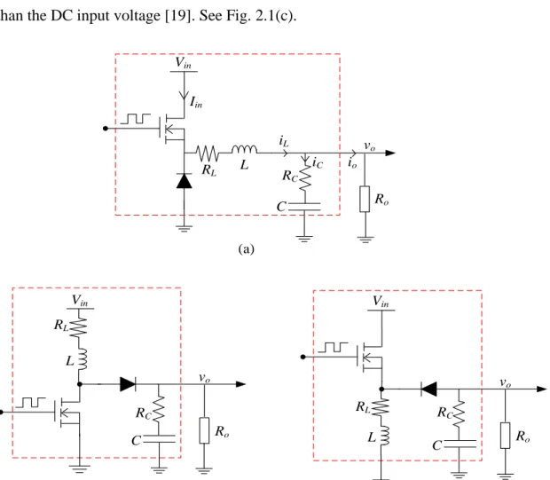
Configuring the components of dc-dc converters in different ways will lead to the forming of various power circuit topologies (Fig. 2.1). All of the circuit topologies have the same types of components including capacitor (C), inductor (L), load resistor
(Ro), and the lossless semiconductor components. The selection of the topology is mainly dependent on the desired level of regulated voltage, since the dc-dc converters are applied to produce a regulated DC voltage with a DC level different from the input DC voltage. This level can be higher or lower than the DC input voltage. However, the most widely used SMPCs are known as: buck converter, boost converter and buck-boost converter. A dc-dc buck converter is configured to generate a DC output voltage lower than the input voltage, Fig. 2.1(a). Conversely, a dc-dc boost converter is utilised to provide a DC output higher than the applied input voltage, as shown in Fig. 2.1(b). Finally, a dc-dc buck-boost converter is able to produce two levels of DC output voltage; these levels can either be lower or higher than the DC input voltage [19]. See Fig. 2.1(c).
Vin Iin L C io Ro vo iL iC RC Vin L C Ro vo RL RC Vin L C Ro vo RL R C (a) (b) (c) RL
Fig. 2.1 Most common dc-dc converter topologies, a: buck converter, b: boost converter, c: buck-boost converter
2.2.1DC-DC Buck Converter Principle of Operation
The buck converter is employed to step down the input voltage (Vin) into a lower output voltage (Vo). This can be achieved by controlling the operation of the power switches (e.g. MOSFET), usually by using a PWM signal. Accordingly, the states of the switch (On/Off) are changed periodically with a period equal to Tsw (switching period) and conversion ratio (duty-cycle) equal to D. The level of the converted DC voltage is based on the magnitude of the applied input voltage and the duty ratio. During the steady-state, the duty cycle is calculated by D = Vo / Vin [19]. Then, the L
-C low pass filter removes the switching harmonics from the applied input signal. In practice, to deliver a smooth DC voltage to the connected load, the selected corner frequency of this filter should be much lower than the switching frequency (fsw) of the buck converter [18]. This corner frequency is defined as:
LC fo 2 1 (2.1)
Two switching states are apparent during each switch period. The first state is when the switch is On and the diode is Off. At this state, the input voltage will pass energy to the load through the inductor and the storage elements start to charge. The second state is when the switch is Off and the diode is On; then the stored energy will discharge through the diode. This operation is known as a Continuous Conduction Mode (CCM). In CCM the inductor current will not drop to zero during switching states, whilst in second operation mode which is Discontinuous Conduction Mode (DCM), the inductor current drops to zero before the end of the switching interval. As a result, a third switching state is introduced during the switching period. In this state, the inductor current drops and remains at zeros while both the diode and switch are
Off during the operation interval [19]. 2.3DC-DC Buck Converter Modelling
In order to design an appropriate feedback controller, it is essential to define the model of the system. Accordingly, this section presents the details of analysis and modelling of the dc-dc converter. This research focuses on modelling and control of the synchronous dc-dc buck converter, as this topology is widely used in industrial
and commercial products [10, 12]. In synchronous dc-dc buck converter the free-wheel diode is replaced by another MOSFET device. A point of load (POL) converter is one of the applications that utilises this kind of topology. As previously mentioned, there are two intervals per switching cycle. The switching period is defined as the sum of the On and Off intervals (Tsw = Ton + Toff). The ratio of the Ton interval to the switch period is known as the duty ratio or duty cycle (D = Ton / Tsw). In the steady- state operation, the output voltage can be computed in terms of duty cycle. The buck dc-dc converter produces a lower output voltage compared with the input voltage (2.2). As expressed in (2.2), the variation of the output voltage magnitude is controlled by the Ton duration or duty cycle value. The PWM signal is used to control the output voltage level [19].
in in sw on o V DV T T V (2.2)
During the Ton duration, the circuit diagram of the buck converter can simply be depicted as in Fig. 2.2(a). A set of differential equations are derived to describe this period of operation: ) ( L C L C C o in L V R R i v R i dt di L (2.3) o o L o L C R v i i i dt dv C (2.4) C C C C o L C o v dt dv C R v i i R v ( ) (2.5)
Generally, the dc-dc converter model is defined by state-space matrices [21]:
in in V t y V t 1 1 1 1 ) ( ) ( E x C B x A x (2.6)
Here, A1, B1, C1, and E1are the system matrices/vectors during the On interval, y is the output, and x(t) is the capacitor voltage and inductor current state vector:
By substituting equation (2.4) into (2.5) and solving with respect to the output voltage (vo), the output vector can be written in state space matrix form as:
L C C o C o C o o i v R R R R R R R x C y 1 (2.7) Now, inserting equations (2.3)-(2.5) into (2.6), the On state space matrix A1 and vector B1 can be expressed as [21]:
L R R R R R L L R R R R R R C R R C C o C o L C o o C o o C o 10 , 1 ) ( ) ( 1 ) ( 1 1 1 B A (2.8) Vin L C io Ro − iL iC RL RC vC + vo L C io Ro − iL iC RL RC vC + vo (a) (b)
Fig. 2.2 Buck converter circuit configuration, a: On state interval, b: Off state interval In the second interval, during the Toff duration, the system equations of the buck converter have the same form with Ton interval. The only difference between the On and Off duration is the B vector (2.9). Fig. 2.2(b) presents the circuit diagram of the buck converter during the Off interval.
0 , 0 , 1 0 , 2 1 2 1 2 1 2 1 E E C C B B A A C o C o C o o R R R R R R R L (2.9)
Finally, the state space matrices during Off duration can be written as: in in V t y V t 2 2 2 2 ) ( ) ( E x C B x A x (2.10) 2.4Model Simulation
To investigate the behaviour of the aforementioned buck model, the derived differential equations presented in section (2.3) have been simulated using MATLAB/Simulink. The power load of the designed dc-dc buck converter is for 5 W operations. The following circuit parameters are used: L = 220 µH, C = 330 µF, Ro = 5Ω,RL = 63 mΩ,RC =25mΩ,Vin = 10 V, and the switching frequency is 20 kHz. These parameters are calculated using design notes available from Microchip(TM) [22]. Fig. 2.3 and Fig. 2.4 shows the open loop output voltage and inductor current at 33% duty-cycle and Vin = 10 V. As displayed in the waveforms of Fig. 2.3 and Fig.
2.4, the steady state DC output voltage and the inductor are evidently content periodic ripples that are repeated at each switching period. Normally, the power stage elements (L, C) determine the magnitude of the ripple as shown in the waveforms.
Fig. 2.3 Open loop steady state output voltage
0.04 0.0401 0.0402 0.0403 0.0404 0.0405 3.28 3.285 3.29 3.295 3.3 3.305 3.31 Time (s)
Fig. 2.4 Open loop steady state inductor current 2.5Buck State Space Average Model
The state space average model is the most common approach to obtain the linear time invariant (LTI) system of SMPC. The strategy starts by averaging the converter’s waveforms (inductor current and capacitor voltage) over one switching period to produce the equivalent state space model. In this way, the switching ripples in the inductor current and capacitor voltage waveforms will be removed [23]. As demonstrated in the previous section, there are two LTI differential equations to describe the operation of buck dc-dc converter (On and Off intervals). By averaging these two state intervals, the state space average model can be obtained. This is achieved by multiplying the On interval (2.6) by d(t) and the Off interval (2.10) by
Off time duration [d`(t) = 1 −d(t)]. This yields the following state space average model [18]:
in in V t d t d t t d t d t V t d t d t t d t d 2 1 2 1 2 1 2 1 ) ( 1 ) ( ) ( ) ( 1 ) ( ) ( ) ( 1 ) ( ) ( ) ( 1 ) ( E E x C C y B B x A A x (2.11)where, d denotes the On time length.
Once the average state space model of the buck converter is defined, it is possible to apply the Laplace transform for obtaining the frequency domain linear time model.
0.04 0.0401 0.0402 0.0403 0.0404 0.0405 0.3 0.4 0.5 0.6 0.7 0.8 0.9 Time(s)
This model is essential in the linear feedback control design, such as the root locus control approach. In voltage mode control of the SMPC, the control-to-output voltage transfer function (2.12) [24, 25] plays the important role of describing the locations of poles/zeros for optimal voltage response. The control-to-output model can be computed by applying the Laplace transform to the small signal average model of SMPC in equation (2.11) and then solving the system with respect to output voltage. This research is primarily focused to utilise this model in the system identification and the power converter control design.
1 1 ) ( 2 L o L o L o C L o C o C in dv R R L R R R R C C R s R R R R LC s s CR V s G (2.12)As expressed in (2.12) the control-to-output transfer function of the buck SMPC exhibits a general form of second order transfer function and generally it can be written as [1, 18]: 2 1 1 ) ( o o zesr o dv w s Qw s w s G s G (2.13)
where, the corner frequency (wo) of the buck converter, the quality factor (Q), the zero frequency (wzesr), and the dc gain (Go) can be defined as follows [26]:
C zesr in o L o L o L o C o C o L o o CR w D Vo V G R R C R R R R L C R w Q R R LC R R w 1 1 ) ( (2.14)
From equation (2.13), it can be observed that the control-to-output voltage transfer function of the buck converter contains two poles and one zero. The locations of the poles as well as the dynamic behaviour of the dc-dc converter are mainly dependent upon the quality factor (Q) and the angular resonant frequency (wo) of the converter. In the time domain, the quality factor gives indication of the amount of overshoot that occurs during a transient response. This factor is inversely related to the damping ratio (ξ) of the system [27, 28]:
2 1 , 2 4 1 1 / 2 Q e M Q Q p (2.15)
Here, MPisthe maximum peak value.
It is worth noting that a non-negligible resistance of the output capacitor (RC) of the dc-dc converter introduces a zero in the control-to-output voltage transfer function of the SMPC as given in (2.13). The location of this zero has a negative impact on the dynamic behaviour of the SMPC. In order to cancel the effect of this zero and improve the system performance, a constant pole in the control loop may be added. This pole can be placed at the same value as the ESR zero.
2.6Discrete Time Modelling of Buck SMPC
In order to derive the discrete model of SMPC, the continuous time dynamic model in (2.6) and (2.10) should first be defined. Then, by sampling the states of the converter at each time instant, the continuous time differential equations are transformed into a discrete time model. A discrete time model is necessary for digital implementation of the algorithms. In the literature, different techniques have been proposed for discrete time modelling of dc-dc converters and for obtaining the control-to-output transfer function [21, 29]. However, these techniques including the direct transformation methods (bilinear transformation, zero-order-hold transformation, pole-zero matching transformation, etc.) from s-to-z domain are generally describe the buck SMPC as a second order IIR filter (2.16), for example the literature that have been presented in [1, 5, 21, 30-33].
2 , 1 ) ( 2 2 1 1 2 2 1 1 N M z a z a z a z b z b z b z G M M N N dv (2.16)
However, a zero-order-hold (ZOH) transformation approach is preferred for discrete time modelling of the control-to-output transfer function (2.17). Practically, the sampled data signals are acquired based on sample and hold process followed by A/D operation. In addition, the control signal remains constant (held) during the sampling interval and is modified at the beginning of each updated cycle [30]. Therefore, both the control and output signals are based on ZOH operation. Consequently, a ZOH transformation method is utilised in this work. The authors in [30] and [31] use the ZOH transformation method to model the Gdv(z) and then to be used in the system identification process. Recently, system identification techniques have been extensively used in dc-dc converters for discrete time modelling of small signal control-to-output transfer function. This is typically accomplished by superimposing the duty command with a small amplitude signal. The frequency components and the amplitude are then estimated through different identification methods. Finally, the frequency response control-to-output LTI transfer function can be constructed. Other approaches involve by directly identifying the z-domain transfer function using different parametric identification techniques such as the RLS algorithm. s s G Z z z Gdv( ) (1 1) dv( ) (2.17)
2.7Digital Control Architecture for PWM DC-DC Power Converters
Digital controllers have been increasingly used in different fields and have recently become widely utilised in the control design of SMPCs. The use of digital controllers can significantly improve the performance characteristic of dc-dc converters for several reasons. Firstly, digital controllers provided more flexibility in the design compared with the analogue controllers. Secondly, they can be implemented with a small number of passive components, which reduce the size and cost of design. Also, digital controllers have low sensitivity on external disturbances and system parameter
variations. In addition, digital controllers are easy and fast to design, as well as to modify or change the control structures or algorithms. Furthermore, it enables advance control algorithms to be implemented, such as non-linear control, adaptive control, and system identification algorithms. Finally, programmability; the algorithms can easily be changed and reprogrammed [34-36]. On the other hand, the power processing speed is faster in an analogue controller than in a digital controller; this is due to the limitations in the microprocessors speeds. Furthermore, the system bandwidth is higher in analogue design compared with the digital design. In addition, no quantisation effects are considered in analogue systems [37, 38]. However, in order to stabilise the output voltage at the desired level, the control signal must be varied and accommodate any changes in the system, such as load changes or the variations in the input voltage. This can be performed by designing an appropriate feedback controller for appropriate control signal generation.
There are two common control structures applied in the closed loop control design of the dc-dc power converters: voltage mode control and current-mode control. Digital voltage mode controllers are mostly used and preferred in the industry over current-mode controllers [10-12]. This is because the current-mode controllers require an additional signal condition circuit, consisting of a high speed current sensor; in consequence this will incur extra costs to the system [39]. In addition, a voltage mode control is simple to design. Therefore, this research will concentrate on the design and implementation of the digital voltage mode control for SMPCs.
2.7.1Digital Voltage Mode Control
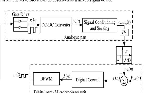
As illustrated in Fig. 2.5, the digitally controlled voltage mode scheme of SMPCs is divided into six sub circuit blocks. These circuits are categorised into two parts. The first part defines as an analogue system, including the dc-dc power processor stage, the gate drive, and the sensing/signal conditioning circuits. The second part classifies as the digital system, which is represented by the digital controller, and DPWM. The ADC block can be described as a mixed signal device.
Analogue part
Signal Conditioning
and Sensing
v
o(
n
)
V
ref(
n
)
e
(
n
)
d
(
n
)
DPWM
DC-DC Converter
+
A/D
Digital Control
c
(
t
)
v
sensing(
t
)
Digital part \ Microprocessor unit
Gate Drive
g
(
t
)
−
v
o(
t
)
Hs
Fig. 2.5 Digital voltage mode control architecture of DC-DC SMPC
The output voltage generated from the dc-dc power converter is firstly sensed and scaled via a commonly used resistive voltage divider circuit with gain factor equal to
Hs. Hence, any sensed voltage higher than the ADC full dynamic scale must be attenuated by a factor to be processed within the desired range. Other signal conditioning circuits can also be considered for suitable interfacing with ADCs. This includes different analogue circuits such as buffer circuits with wide bandwidth operation. An anti-aliasing filter is often used to filter the frequency content in the output voltage that is above half of the ADC sampling frequency (Nyquist criteria) [11]. Typically, this would be a low-pass filter.
The sensed output voltage (vsensing) is digitised by the ADC. In digital control design for SMPC, there are two factors that must first be considered for the appropriate selection of an ADC:
1) The A/D number of bits or A/D resolution. This is important to the static and dynamic response of the controlled voltage of SPMC. The A/D resolution has to be less than the allowed variation in the sensed output voltage [40, 41].
2) The conversion time is an important factor in the selection of ADC as it dictates the maximum sampling rate of the ADC. In digitally controlled SMPCs, the conversion time is required to be small enough to achieve a fast response and high dynamic performance. Typically, the sampling time of an ADC is chosen to be equal to the switching frequency of the SMPC. This will ensure that the control signal is updated at each switching cycle.
The digital reference signal, Vref(n) is compared with the scaled sampled output voltage, vo(n). The resultant error voltage signal, e(n), is then processed by the digital controller via its signal processing algorithm. A second order IIR filter is used as a linear controller that governs the output voltage of the SMPC as described in (2.18) and shown in Fig. 2.6 [20]. Generally, this IIR filter performs as a digital PID compensator as a central controller in the feedback loop. Both non-linear control and intelligent control techniques can also be applied for the digital control of SMPCs [24, 42-45].
M k k k N i i c z s z i q z G 1 0 1 ) ( (2.18)However, the control signal, d(n), is then computed on cycle-by-cycle basis. The desired duty ratio, c(t), of the PWM is produced by comparing the discrete control signal with the discrete ramp signal; in the digital domain it is represented as a digital counter. Here, the DPWM performs as an interface circuit between the digital and analogue domains of the digitally controlled architecture within the SMPC,
simulating the purpose of the digital-to-analogue converter (DAC). Finally, the generated On/Off command signal across the DPWM is amplified by the gate drive circuit. The output of the gate signal is then used to activate the power switches of the SMPC. z-1 e(n) e(n-1) d(n) z-1 z-1 z-1 e(n-2) d(n-1) d(n-2) q0 q1 q2 -s1 -s2 + + + + + ++ +
Fig. 2.6 Two-poles / Two-zeros IIR digital controller
It is worth noting that a high resolution DPWM is essential for the digital control of SMPCs. This will lead to accurate voltage regulation and avoid the limit cycle oscillation phenomenon. Limit cycles are defined as non-linear phenomena that occur in digital control of dc-dc converters during steady-state periods. In accordance to [46], the undesirable limit cycle oscillations in digitally controlled dc-dc converters can be avoided when the DPWM resolution is greater than the ADC resolution. Therefore, in order to eliminate the limit cycle oscillations, the resolution of DPWM has to be at least one bit greater than the ADC resolution [46]. Also, care is required in the selection of the integral gain in PID controllers, as excessively high values of integral gain can cause limit cycle oscillations around the steady-state value. For more rigorous details and analysis of the limit cycle oscillation, the reader should refer to the work presented by Peterchev and Sanders[46].
2.8Digital Proportional-Integral-Derivative Control
The digital PID controller is well known and it is commonly used in control loop design of SMPCs [47]. This is because the PID control parameters are easy to tune and the designed controller is easy to implement. Generally, the discrete PID controller can be described as given by (2.19) [48]. Here, the PID controller is in
parallel form structure, where the control action is divided into three control signals as shown in (2.20) and the PID gains can be tuned independently.
) 1 ( 1 1 ) ( ) ( ) ( 1 1 K z z K K z E z D z Gc P I D (2.19) ) ( ) ( ) ( ) (n d n d n d n d P I D (2.20) where:
( ) ( 1)
) ( ) 1 ( ) ( ) ( ) ( ) ( n e n e K n d n d n e K n d n e K n d D D I I I p p (2.21)The variables KP, KI, and KD, are the proportional-integral-derivative gains of PID controller, e(n) is the error signal [e(n) = Vref(n) −vo(n)], and d(n) is the control action. From (2.19), the discrete time domain of the PID controller can be described as shown in Fig. 2.7 and given in (2.22) and (2.23):
) 2 ( ) 1 ( ) ( ) 1 ( ) (n d n q e n q1e n q2e n d o (2.22) D D P D I P o K q K K q K K K q 2 1 ( 2 ) (2.23) z-1 e(n) e(n-1)
e(n-2) q0 d(n) z-1 z-1 q1 q2