CIRCUITS AND SYSTEMS FOR WIRELESS
CONCURRENT COMMUNICATION
Thesis by Yu-Jiu Wang
In Partial Fulfillment of the Requirements for the Degree of
Doctor of Philosophy
CALIFORNIA INSTITUTE OF TECHNOLOGY Pasadena, California
2009
© 2009
Yu-Jiu Wang
Acknowledgements
I would like to express my sincerest gratitude to my research advisor, Professor Ali Hajimiri, for his excellent guidance, encouragement, and patience during the years of my Ph.D. Ali is not only my advisor, but also my role model. From him, I have learned how to improve myself consistently, how to treat my promises seriously, how to dedicate myself to my profession, and how to think and live independently. I am in particular grateful to his tolerance of the many troubles I made for him in the past four years and five months.
I would like to thank Professor Sander Weinreb for his technical support and assistance over the course of my Ph.D. In particular, I am grateful for his technical inputs during the concurrent phased array project and the modified FET noise models project.
I would also like to thank Professor Ali Hajimiri, Professor Sander Weinreb, Professor Dave Rutledge, Professor Azita Emami, and Professor P.P.Vaidyanathan for serving on my candidacy and defense committees.
I would like to thank all members of Caltech High Speed Integrated Circuits, Caltech Millimeter-Wave IC, and Caltech Mixed-Mode Integrated Circuits and Systems groups. I am particularly thankful to Dr. Aydin Babakhani for making the early part of my Ph.D. “extraordinary”, as well as providing many interesting ideas regarding both research and lifestyles. I would also like to thank Hua Wang, for discussing many technical questions with me, and helping me with many experiments and designs. He is also a good friend to talk about different general issues, and to have “ordinary” fun. I would also like to thank Dr. Xiang Guan, Dr. Arun Natarajan, Dr. Behnam Analui, Dr. Abbas Komijani, Professor Ehsan Afshari, Sam Mandegaran, Professor Jim Buckwalter, Professor Arjang Hassibi and Dr. Chris White for their memtoring during the early part of my Ph.D. I wish to thank my colleagues Professor Sangguen Jeon, Florian Bohn, Edward Keehr, Juhwan Yoo, Jay Chen, Jennifer Arroyo, Kaushik Sengupta, Steven Bowers, Kaushik Dasgupta, Alvaro Gonzales, and Tomoyuki Arai from Fujitsu for their support. I also wish to thank Yu-Lung Tang, Matthew Loh, and Joe Bardin in the fourth floor for their help.
I would like to thank Michelle Chen, Dale Yee, Naveed Near-Ansairi, John Lilley, Hamdi Mani, Niklas Wadefalk, Ann Shen, Linda Dozsa, Tanya Owen, Carol Sosnowski, Gary Waters, Lynn Hein, Janet Couch, and Kent Porter for their valuable assistance during my time at Caltech.
Professor Chin-Lin Guo, Ray Huang, Professor Hsuan-Tien Lin, Chun-Hui Lin, Mingshir Lin, Sebastien Lasfargues, Shafigh Shirinfar, John Howard, and Richard Ohanian.
I would also like to thank Professor Huei Wang at National Taiwan University who brought me to this exciting field ten years ago, so I would have the chance to write this thesis. I would also like to thank Professor Ming-Juey Lin in National Taiwan Normal University, who chose me to the International Physics Olympiad national team, and showed me how large the world is during my high school years.
Abstract
Concurrency is a special kind of analog circuit parallelism that uses a single circuit with necessary bandwidth to process multiple signals at the same time. Concurrent radios offer a higher data rate and improved system diversity. Our comprehensive treatment comprises proposals for potential transceiver architectures, invention of circuit blocks, and provisions of innovative analysis methods.
The analysis of concurrent circuits are often complex. To simplify noise analysis, a
-vector space is first proposed to re-formulate the N-port network noise modeling problem. Any internal physical source inside the noisy network contributes a small vector
in the defined -vector space, and the aggregate statistical behavior of this noisy network can be viewed as the vector sum of these vectors. Applying this concept to FET noise modeling leads to several modified FET noise models, in which three uncorrelated noise sources are sufficient to describe the statistical behavior of an intrinsic FET. The use of these new FET models can simplify the analysis, simulation, and optimization of low noise systems without sacrificing accuracy.
consumption. A compact 3.1─10.6 GHz WDA IC is built on a 130 nm CMOS process. Experimental results show 2.3─4.5 dB NF at 23 mW power consumption.
Using concurrency in wireless link can boost communication data rate. As a proof-of concept, we propose dynamically scalable concurrent communication by dividing the 7.5 GHz bandwidth of the unlicensed 3.1─10.6 GHz spectrum into seven concurrent channels. A CMOS octa-core RF receiver is implemented to validate the idea. Based on the receiver measurement results, a wireless link can be built to achieve a 16 Gbps channel limit at five meter TX-RX distance at 400 mW power consumption.
Tunable concurrency can improve the receiver diversity. A prototype 6─18 GHz concurrent tunable dual-band phased array receiver element IC is proposed and built on a 130 nm CMOS process. Experimental results demonstrate successful dual-band RF reception within a low band (6─10.4 GHz) and high band (10.4─18 GHz) with 300 MHz baseband bandwidth. A final four-element phased array receiver built from the prototyped ICs shows an array pattern with worst-case 21 dB peak-to-null ratio across all frequencies.
Table of Contents
Acknowledgements ... iv
Abstract ... vii
Table of Contents ... ix
Chapter 1: Introduction ... 1
1.1. Organization ... 2
Chapter 2: Noisy Network Modeling Using Only Uncorrelated Sources .. 5
2.1. Circuit Theory of Linear Noisy Network ... 7
2.2. Defining Vector Space for Linear Noisy Network ... 9
2.3. Example: A Two-Port Noisy Network ... 15
2.4. A Modified FET Noise Model ... 20
2.5. FET Noise Model Comparisons ... 23
2.6. Summary ... 27
Appendix 2.1: Van der Ziel’s FET Noise Model ... 28
Appendix 2.2: Pospieszalski’s Noise Model ... 35
Appendix 2.3: BSIM4 Noise Model ... 36
Chapter 3: A Compact Low Noise Weighted Distributed Amplifier ... 37
3.1. Input Matching versus Bandwidth ... 38
3.2. Issues of Power-Constraint LNA Optimization in CMOS ... 40
3.3. Low-Noise Distributed Amplifier ... 42
3.4.1. Noise from Common-Source Transistors ... 46
3.4.2. Noise from Cascode Transistors ... 49
3.4.3. Noise from Termination Resistors ... 51
3.4.4. Noise from Passive Network Loss ... 52
3.4.5. Voltage Peaking Effect in LC-Ladder ... 54
3.4.6. Frequency-Dependent Group Delay ... 56
3.4.7. Frequency-Dependent Impedance Change ... 57
3.4.8. Noise Figure of WDA... 58
3.5. Power-Constraint Noise Optimization of WDA ... 59
3.6. Magnetic Couplings in LC-Ladder ... 61
3.7. WDA Schematics and Layout ... 64
3.8. WDA Measurement Results ... 68
3.9. Summary ... 72
Appendix 3.1: Integrated RF VLSI Design Flow ... 73
Chapter 4: Concurrent Octa-Core RF Receiver Architecture ... 77
4.1 Introduction ... 78
4.1.1 Wireless Multi-Gbps Communication ... 78
4.1.2 Comparisons between the 3.1─10.6 GHz and the 60 GHz Band ... 80
4.1.3 Previous Works using the 3.1─10.6 GHz Band ... 80
4.2 A 3.1─10.6 GHz Octa-Core Receiver ... 82
4.2.1 System Architecture ... 82
4.2.3 Downconversion Core: PLL, Mixers, and BB Buffers ... 88
4.2.4 Experimental Results ... 91
4.3 Summary ... 99
Chapter 5: Scalable Concurrent Dual-Band Phased Array Receiver ... 100
5.1. Introduction of Phased Array Receiver ... 101
5.1.1. Limitations of Previous Works on Phased Array ... 103
5.1.2. Previous Works on Concurrent Dual-Band Receivers ... 105
5.1.3. Proposed Large-Scale Phased Array System Architecture ... 105
5.2. Tunability of Concurrent Dual-Band Amplifiers ... 108
5.3. Tunable Concurrent Amplifier (TCA) ... 112
5.3.1. Common-Gate Common-Gate (CG-CG) Topology ... 113
5.3.2. Common-Gate Common-Source (CG-CS) Topology ... 114
5.3.3. Resistor Termination Topology ... 116
5.3.4. Active Termination Topology ... 117
5.4 A 6─18 GHz Concurrent Tunable Dual-Band Phased Array Receiver ... 121
5.4.1 Block Diagrams ... 121
5.4.2 TCA ... 124
5.4.3 RF and IF Mixers ... 125
5.4.4 Baseband Buffers ... 127
5.4.5 Whole Receiver Chip ... 128
5.5 Experimental Results ... 129
5.5.2 Four-Element Phased Array Pattern ... 134
5.6 Summary ... 138
Chapter 6: Concurrent Co-Channel Dual-Beam Phased Array Receiver
... 139
6.1. Dual-Beam Phased Array System Architecture ... 140
6.2. A 10.4─18 GHz Concurrent Quad-Beam Phased Array Receiver ... 142
6.2.1. Receiver Element Block Diagrams ... 142
6.2.2. LNA ... 144
6.2.3. IF Signal Distribution Networks ... 146
6.2.4. RF/IF Mixers and Baseband Buffers ... 146
6.2.5. Receiver Element Implementation ... 146
6.3. Experimental Results ... 148
6.3.1. Receiver Element Measurement Results... 148
6.3.2. Four-Element Phased Array Measurement Results ... 150
6.4. Summary ... 156
Chapter 7: Conclusion ... 158
7.1 Summary ... 158
List of Figures
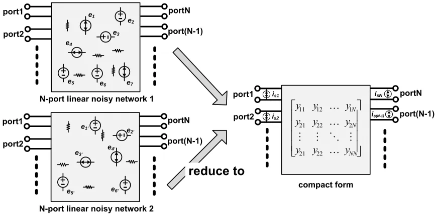
Figure 2.1: Different noisy networks might be able to reduce to the same compact network form. ... 9
Figure 2.2: Noise contributions from the internal physical noise sources to the external world can be interpreted as the sum of several noise vectors in the defined vector space. ... 13
Figure 2.3: Two correlation admittances are used to decorrelate the two noisy sources. .... 16
Figure 2.4: A controlled source is used to implement a noisy two-port network. ... 16
Figure 2.5: (a) A physical two-port linear noisy network, (b) Compact form of a two-port noisy network, (c) A two-port network with four uncorrelated noise sources, and (d) The conceptual plots of the noise vectors for (a) and (c) in an R4-space ... 18
Figure 2.6: Three frequency-independent and uncorrelated sources are used to implement Van der Ziel’s FET noise model. ... 21
Figure 2.7: Another modified FET noise model is also equivalent to Van der Ziel’s FET noise model. ... 23
Figure 2.8: Pospiezalski’s model, BSIM4 model, and modified FET noise model are fitted to the long-channel Van der Ziel’s model. ... 25
Figure 2.9: FET noise modeling is viewed as vector summation in the normalized vector space. ... 27
Figure 2.10: Linear voltage perturbation distribution along the channel of a FET due to a noise perturbation at x0 ... 28
Figure 3.1: Signal strength in wireless communication ... 37
Figure 3.2: Trade-offs for input matching and input parasitic capacitance ... 40
Figure 3.3: Transconductance current efficiency and fT versus bias voltage of a CMOS transistor and an intrinsic BJT ... 42
Figure 3.4: The concept of distributed amplification ... 43
Figure 3.5: The concept of weighted distributed amplifier ... 45
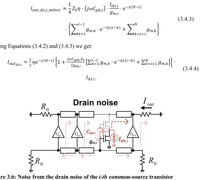
Figure 3.6: Noise from the drain noise of the i-th common-source transistor ... 47
Figure 3.7: Noise from the gate noise of the i-th common-source transistor ... 48
Figure 3.8: Noise from the source noise of the i-th common-source transistor ... 48
Figure 3.9: Noise from the drain noise of the i-th cascode transistor ... 49
Figure 3.10: Noise from the gate noise of the i-th cascode transistor ... 50
Figure 3.11: Noise from the source noise of the i-th cascode transistor ... 51
Figure 3.12: Equivalent circuit of the LC-ladder with a lossy inductor between the (i-1)-th and i-th stage ... 52
Figure 3.13: Driving the LC-ladders with a broadband power source, and its equivalent circuit ... 55
Figure 3.14: Driving the output LC-ladder from an internal load, and its equivalent circuit56 Figure 3.15: Power-constraint noise optimization contour comparisons between a DA and a WDA ... 59
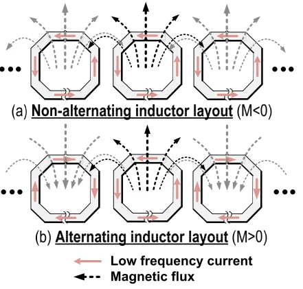
Figure 3.16: Adjacent couplings in a LC-ladder ... 62
Figure 3.17: Inductor layouts in two different LC-ladders: (a) Non-alternating inductor layout, and (b) Alternating inductor layout ... 63
Figure 3.19: Schematics of the intermediate amplifiers and their device sizing ... 65
Figure 3.20: Schematics of the variable termination resistors ... 66
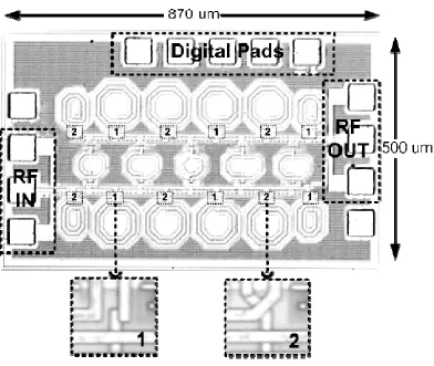
Figure 3.21: Die micrograph of the WDA ... 67
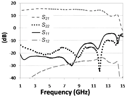
Figure 3.22: S-parameters measurement results ... 68
Figure 3.23: Noise figure (NF), referred third-order intercept point (IIP3), and input-referred 1 dB gain compression point (P1dB) measurement results at 26 mW .. 69
Figure 3.24: Measured noise figure (NF) and simulated NF of different transistor at 17 mW power consumption ... 70
Figure 3.25: Worst-case measured performance versus power consumption ... 71
Figure 3.26: Conventional RF IC design flow ... 73
Figure 3.27: An integrated RF VLSI design flow ... 75
Figure 4.1: Previous works on the 3.1─10.6 GHz band: (a) Impulse-band and (b) Frequency-hopping based ... 81
Figure 4.2: Dynamically scalable concurrent communication ... 82
Figure 4.3: System architecture of proposed octa-core RF receiver ... 84
Figure 4.4: Schematics of the RF common part ... 88
Figure 4.5: Block diagram of the down-conversion core ... 90
Figure 4.6: Chip micrograph of the octa-core receiver IC ... 91
Figure 4.7: Schematics of mixer and RF/LO-I buffers inside each RX core, and the results of system healing at a typical VGA gain setting ... 92
Figure 4.8: Measured receiver maximum conversion gain and S11 ... 94
Figure 4.10: Measured cross-band rejection ... 95
Figure 4.11: Measured LO spurs and core-to-core LO leakage ... 96
Figure 4.12: Channel capacity of a wireless link built with the octa-core receiver, with a transmitter transmitting at FCC’s spectrum mask and isotopic antennas for both RX and TX ... 97
Figure 5.1: Basic phased array receiver configuration ... 101
Figure 5.2: A conventional way of building a large-scale phased-array receiver system (in the active array configuration) that supports concurrent multiple beams... 104
Figure 5.3: A proposed 6–18 GHz phased array receiver system that receives four beams at two frequencies concurrently and is easily scalable toward a very large-scale array ... 106
Figure 5.4: Schematics of a concurrent dual-band amplifier ... 109
Figure 5.5: Achievable frequency region of tunable dual-band operation of the amplifiers in Figure 5.4 with limited capacitor tuning range, and all frequencies between 6─ 18 GHz covered by either band ... 111
Figure 5.6: Schematics of a common-gate common-gate TCA ... 112
Figure 5.7: Schematics of a common-gate common-source TCA ... 114
Figure 5.8: Schematics of a resistor-terminated TCA ... 116
Figure 5.9: Schematics of an active-termination TCA ... 117
Figure 5.10: Architecture of the tunable concurrent dual-band quad-beam phased array receiver in CMOS ... 122
Figure 5.12: Schematic of the TCA with a single input and a dual output ... 123
Figure 5.13: Schematic of the RF mixer and IF buffer for LB ... 125
Figure 5.14: Schematic of the RF mixer for HB ... 126
Figure 5.15: Schematic of baseband VGA ... 127
Figure 5.16: Chip micrograph ... 128
Figure 5.17: Block diagram of the receiver measurement setup ... 129
Figure 5.18: Measured input-matching performance ... 130
Figure 5.19: Measured conversion gain ... 131
Figure 5.20: Measured nonlinearity performance: Input-referred IP3 and 1 dB compression132 Figure 5.21: Measured noise figure of the CMOS receiver (solid line with markers) and the complete system including the active antenna module (dashed line) ... 132
Figure 5.22: Measured isolation performance: Cross-band and cross-polarization rejection ratios ... 133
Figure 5.23: Photo of the four-element array ... 134
Figure 5.24: Electrical array test setup ... 135
Figure 5.25: Measured array patterns of the four-element array. Theoretical patterns are superimposed. ... 136
Figure 6.1: Architecture of the 10.4 – 18 GHz co-channel dual-beam phased array receiver system ... 140
Figure 6.2: Architecture of the tunable co-channel dual-beam phased array receiver element in CMOS (10.4─18 GHz). ... 143
Figure 6.4: Schematic of the tunable amplifier ... 145 Figure 6.5: Chip micrograph of the 10.4 ─18 GHz dual-beam receiver element ... 147
Figure 6.6: Measured conversion gain and input-matching performance of the 10.4─18 GHz dual-beam receiver element ... 148
Figure 6.7: Measured input-referred 1 dB gain compression and the IP3 of the 10.4─18 GHz dual-beam receiver element. ... 149
Figure 6.8: Measured noise figure of the 10.4─18 GHz dual-beam receiver element ... 150
Figure 6.9: Concurrent co-channel dual-beam feed with different DOAs ... 151
Figure 6.10: Measured concurrent dual-beam array patterns at 17.85 GHz of the 10.4─18 GHz co-channel dual-beam phased array. The beam-pointing angle for beam 1 (dashed line) is fixed at 0°. The beam-pointing angle for beam 2 (solid line) is steered at (a) –60°, (b) –30°, (c) 30°, (d) 60°. The antenna spacing is assumed as a half wavelength of the incoming signal. ... 152
Figure 6.11: Measured cross-beam rejection performance (fRF = 17.85 GHz). The incident angle of the desired signal is fixed at 0°. ... 152
Figure 6.12: Desensitization of the array system (fRF = 17.85 GHz) ... 154 Figure 6.13: Measured EVM of the concurrent dual-beam signals, each independently
List of Tables
Table 2.1: Comparisons between FET noise models ... 24
Table 4.1: Measured performance summary of the octa-core receiver ... 98
Table 5.1: Measured performance summary of the scalable concurrent dual-band phased array receiver ... 137
Chapter 1: Introduction
In the history of integrated circuits, there have been so many times that people doubt its future: “Are we approaching the physical limit of lithography?”; “Will gate leakage current stop us from scaling?”; “Will parasitics from metal interconnection dramatically degrade the performance of an advanced process?”; “Will IC become too complex for designers to handle in limited time?”; “Will electronics stop improving/evolving?”; etc. Technological innovations like optical-proximity correction, phase-shift mask, strain silicon, high-K gate oxide, metal gate, low-K dielectric, VLSI synthesis, fast-SPICE algorithm [60], etc., have been invented at a convenient time to solve these issues. At the moment this thesis is written, it is fortunate to see this industry continue to roll at its projected speed without any sign of slowing down. It is the creativity and hardwork of scientists and engineers that expand the frontier of technologies.
single-chip silicon-based solutions that do the same tasks. It is exciting to expect more wireless concepts, products, and applications in the near future.
Two major challenges in wireless broadband communication are how to increase system diversity and how to improve broadband radio spectrum efficiency. In this thesis, we will present a unique view on solving these challenges by using concurrency in analog/RF frontend circuitry. Concurrency is a special type of analog circuit parallelism that uses a single circuit with necessary bandwidth to process multiple signals at a same time. Our treatment comprises of the definition of such novel radios, formulation of their particular characteristics, proposals for potential transceiver architectures, invention of circuit blocks, and provisions of innovative analysis methods. Throughout the discussions, our theoretical findings are verified with experimental implementation of the developed concepts.
The contributions of our study include the development of original concepts and new theoretical findings together with practical implications in the area of integrated broadband concurrent multi-band radio systems.
1.1.
Organization
problem for low-noise system design. A vector space for a general noisy N-port is proposed to visualize the noise modeling process as series of vector summation. A general noisy two-port is used as an example to further explain the idea. Applying the noisy two-port to the modeling of intrinsic FET leads to several possible modified FET noise models, in which three uncorrelated noise sources are sufficient to describe the statistical behavior of an intrinsic FET. A comparison between the proposed modified FET noise model, Van der Ziel’s noise model, Pospieszalski’s noise model, and the BSIM4 model is also presented.
Low-noise amplifier (LNA) is a critical building block in wireless concurrent communication. In Chapter 3, we propose the low-noise weighted distributed amplifier (WDA) topology. A distinct advantage of this topology is its tolerance to input parasitic capacitance which can be utilized to provide electro-static discharge (ESD) protection without sacrificing its noise performance and power consumption. The proposed modified FET noise model is applied to simplify noise analysis, simulation, and optimization of the design of a 3.1―10.6 GHz WDA, and a compact test IC is built on a 130 nm CMOS process. Experimental results will be presented which verify the design.
this architecture to achieve a 16 Gbps channel limit at five meter TX-RX distance at 400 mW power consumption.
Chapter 5 and Chapter 6 apply concurrency in phased array systems to increase its diversity. Chapter 5 introduces the scalable concurrent tunable dual-band phased array receiver. Design challenges against achieving concurrent tunable dual-band RF signal reception will be studied first, and their alternative solutions will be discussed. A prototype 6―18 GHz receiver element IC is implemented on a 130 nm CMOS process. Experimental results of a single receiver element as well as a final four-element phased array receiver will be demonstrated.
A phased array receiver can achieve spatial filtering at the system output; however, it should be noted that information from different incoming angles are intact before the combining of phase-compensated receiver array outputs. Chapter 6 introduces a concurrent beam phased array receiver which utilizes this property to achieve concurrent multi-beam reception. This topology allows us to share the antenna, RF frontend, and LO circuitry. A prototype receiver IC has been implemented and measured to verify the concept. A final four-element phase array receiver is built based on the receiver IC which proves the possibility of concurrent multi-beam reception.
Chapter 2: Noisy Network Modeling Using Only
Uncorrelated Sources
Thermal fluctuations of electric charges inside all conductors generate a measurable physical electrical potential between any two ends of the conductors. This random potential was first observed by Johnson in experiments [1], and later Nyquist postulated a black-body radiation thought experiment to relate its noise voltage power to the resistivity of the conductor. Based on Nyquist’s derivations, the average noise power of
the conductors is 4 Δ for [2]. Here, is the Boltzmann constant, is
the temperature of the resistor, Δ is the measurement bandwidth, is the resistivity, is the frequency of noise in concerns, and is Planck’s constant. If an electrical experiment
is carried at room temperature ( 300 ), 6.24 suggests 4 Δ
holds for microwave and millimeter wave ranges.
For all practical purposes, either time-invariant or time-variant, noise can be viewed as a small signal deviation from the case when noise is absent. Thus, linearization around the operating point is usually utilized to simplify the noise analysis. Circuit theory of linear noisy networks has been thoroughly studied by Haus and Adler for more than fifty years [3]. If so, why would it be worth it to us to dedicate one chapter in this thesis to discuss it?
2.1.
Circuit Theory of Linear Noisy Network
For any arbitrary N-port linear network with internal independent sources, output signals consist of the parts that are linearly proportional to the input signals and the other parts contributed by the internal independent sources. Without the loss of generality, we can express this input-output relationship using the admittance matrix in frequency domain:
. (2.1.1)
is the Laplace-transformed input voltages vector: … .
is the Laplace-transformed output currents vector: … .
is the Laplace-transformed output currents vector due to the independent sources:
… . Superscript operator denotes the transpose of a matrix [4]. Laplace-transform of a time domain signal is defined as [5]:
. (2.1.2)
is the Laplace-transformed admittance matrix:
… …
…
, (2.1.3)
with its matrix element .
If we apply the inverse Laplace-transform to Equation (2.1.1), we will get the time-domain representation of the linear network:
Here, … , … , and
… . And the time-domain admittance matrix will become:
… …
…
. (2.1.5)
The matrix elements of , , , and are the time-domain representations of the original matrix elements. The symbol in Equation (2.1.4) is the matrix convolution operator defined as:
∑ . (2.1.6)
In a linear noisy network modeling problem, these independent sources’ contribution to the outputs are random processes. In general, arbitrary random processes are complex to describe. Fortunately, in the case of electronic thermal noise, wide-sense stationary (WSS) property is held. The statistical behavior of WSS random processes can be fully described by their autocorrelation and cross-correlation functions, which are defined as [6]:
(2.1.7)
. (2.1.8)
If we take the Fourier-transform of the correlation matrix of Equation (2.1.7), we will get the cross-spectral density matrix:
Thus, for any arbitrary linear noisy network, we can reduce it to Equation (2.1.1) and Equation (2.1.4), with the statistical description of its noise behavior given by Equations (2.1.8) and (2.1.9).
2.2.
Defining Vector Space for Linear Noisy Network
Based on the theory introduced in Section 2.1, classical noisy network modeling and analysis approach starts with reducing any given complex network into the compact general form. One application of this general form is to derive the minimum achievable noise figure for a general two-port noisy network by Adler and Haus [3]. In addition, one of the major applications of noisy network modeling is to describe the noise behavior of active devices, like transistors. Van der Ziel reduces the thermal noise contributed by the distributed resistors in a FET’s channel to a two-port general form [7] [8].
Figure 2.1: Different noisy networks might be able to reduce to the same compact
network form.
+
-N-port linear noisy network 1
e1 + -e4 e5 port1 port2 portN port(N-1) + -reduce to port1 port2 portN port(N-1) ⎥ ⎥ ⎥ ⎥ ⎦ ⎤ ⎢ ⎢ ⎢ ⎢ ⎣ ⎡ NN N N y y y y y y y y y K M O M M K K 22 21 2 1 22 21 12 11 e2 e3
e6 e7
is1
is2 is(N-1)
isN
+
-N-port linear noisy network 2
e1' + -e4' e5' port1 port2 portN port(N-1) + -e2' e3'
Often in low-noise circuit designs, we will have to resort to EDA software to help us calculate the noise performance of a complex circuit system. Though reducing an elementary noisy network into a compact general form is neat in its mathematical expression, the correlation terms in Equations (2.1.7) and (2.1.9) between different noise sources are difficult to implement. What has been pointed out before is that it is possible for several different physical noisy networks to be reduced to a same general compact network (see example Figure 2.1). In other words, though these physical noisy networks may have different internal structures and noise sources, their network behaviors and statistical properties will be exactly the same when looking from the external world. Since different noisy network structures have different implementation difficulties, it makes it possible to choose to use the noisy network structure that is easiest to implement. However, we have to answer the problem: How do we find such a network in a systematic way? In order to answer this question, we have to look at the compact noisy network of Equation (2.1.4) from a different perspective.
The independent noise sources , , … in Equation (2.1.4) are physical signals. They can be measured by connecting N ideal current meters to measure their short-circuit currents. This means that , , … are real random processes. Since these random processes are real, their cross-correlation function will satisfy:
.
c ω and c ω are a complex conjugate pair. So the cross-correlation matrix will satisfy:
. (2.2.1)
And the cross-spectral density matrix satisfies:
. (2.2.2)
The operator takes the complex conjugate of the transpose of operand, and gives the adjoint matrix of the operand matrix [4]. In addition, the diagonal elements of the cross spectrum are real, since c ω c ω .
Based on these discussions, we can define for m ,
0 for m n, and for m . And
and are real functions. So, the cross-spectral density matrix can be written as:
……
…
. (2.2.3)
At a given frequency , we can use real values to represent an N-port noisy network’s noise behavior.
network has M uncorrelated noise sources, namely: , , … , . And
0 for . We can calculate the output currents
, , … as functions of these internal noise sources.
t t t
t t t
…
t t t
(2.2.4)
Here, is the impulse response from the internal noise source to the output
short-circuit current with all ports shorted. * is the convolution operator. The power spectral
density of current sources: , , … can be calculated to be:
, ω
.
(2.2.5)
Here, , ω , ω
, and . We use the fact that all
physical networks are causal. Similarly, we can calculate the cross-spectral density of the current sources:
,
.
(2.2.6)
Comparing Equations (2.2.3), (2.2.5), and (2.2.6), we realize that , ,
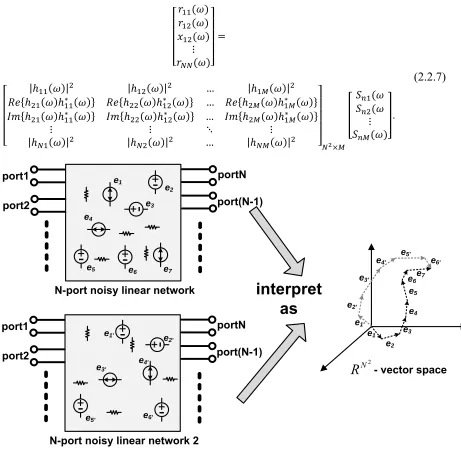
, , and , for . If we define the -tuples
the N-port noisy network can be related to the magnitude of individual internal noise sources by: | | | | … | | … | | | | … … | | . (2.2.7)
Figure 2.2: Noise contributions from the internal physical noise sources to the
external world can be interpreted as the sum of several noise vectors in the defined
vector space.
+
-N-port noisy linear network e1 +
-e4 e5 port1 port2 portN port(N-1) +
-e2 e3
e6 e7
- vector space
2 N
R
e1 e2 e3 e4 e5 e6 e7interpret
as
+Now, if we define the -tuples , , , … , , , , … , , , … , as
-vector space, we can interpret the noise process in the N-port noisy network such that
each internal noisy source contributes a small vector in the defined -vector space. And the total noise behavior of the N-port noisy network is the vector sum of these small vectors contributed by all internal noise sources. In Figure 2.2, we use an example of N-port network with seven internal physical noise sources to demonstrate the concept.
There are several implications of interpreting an arbitrary noisy network in this manner. First of all, if two noisy networks with different internal noise sources accumulate to a same-summed noisy vector, their statistical behavior would be the same from the external world. As shown in Figure 2.2, network 1 and network 2 have different internal structures, and different number of noise sources. The contribution of these noise sources inside the
two noisy networks will correspond to two different “trajectories” in the defined -vector space. However, since their -vector sums point to the same point in the -vector space, network 1 and network 2 have the same statistical behavior.
Now, since a -vector space can be used to interpret an arbitrary N-port noisy network, if we can find a set of noise sources, which are uncorrelated with each other
One final remark before the end of this section: There are several different network representations of an N-port linear noisy network, and in this section, we choose the
admittance matrix representations and define the -vector space based on it. If we choose a different network representation, say the impedance matrix, we will get a different
-vector space. However, they are mathematically equivalent and can be converted to one another by a linear transformation.
In the next section, we will use this concept to model a two-port noisy network as a general two-port example.
2.3.
Example: A Two-Port Noisy Network
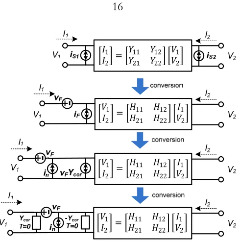
Classical approach of two-port noise modeling reduces a given noisy network into Equation (2.1.1). Due to the correlation between the two elements in
Figure 2.3: Two correlation admittances are used to decorrelate the two noisy sources.
Figure 2.4: A controlled source is used to implement a noisy two-port network.
Another commonly used approach is to separate the second noise source ( ) into a part that is fully correlated with the first noise source ( ) and an other part ( that is totally uncorrelated with , as shown in Figure 2.4. A controlled source is used to introduce the correlation between two correlated noise sources ( and ).
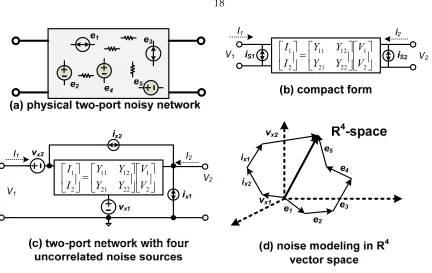
We can also use the concept introduced in Section 2.2 to model an arbitrary noisy network with 4 ( 2 noise sources. As shown in Figure 2.5(a), we have an arbitrary physical two-port linear noisy network, with some arbitrary internal circuit connections and physical noise sources. The classical approach reduces the given network into a compact form shown in Figure 2.5(b) as a basis for circuit analysis. If we define a
-vectors space by grouping ,
we can plot the contributions of the internal noise sources in Figure 2.5(a) in the -vectors space as several small noisy vectors. The overall statistical behavior of the given arbitrary network is thus a vector sum of these smaller noisy vectors, as shown in Figure 2.5(d). It should be noted that, for the convenience of plotting the concept, we use five internal noisy sources for the network in Figure 2.5(a). In general, the number of noise sources inside the noisy network can be arbitrary.
Figure 2.5: (a) A physical port linear noisy network, (b) Compact form of a
two-port noisy network, (c) A two-two-port network with four uncorrelated noise sources, and
(d) The conceptual plots of the noise vectors for (a) and (c) in an R4-space
Since any point in the defined vector space represents a particular statistical behavior, we can find another noisy network with four uncorrelated noise sources to match an arbitrary two-port network’s noise property. In Figure 2.5(c), we show one of the possible network choices. We choose this network topology for the convenience of modeling an FET. In general, we can choose arbitrary four-noise sources as long they are linearly independent in the -space. To model an arbitrary two-port network with the network in Figure 2.5(c), we need to first relate and in Figure 2.5(a) by , ,
, and :
-
. (2.3.1)
Based on Equation (2.3.1), we can calculate the spectral density and the cross spectral density of and in terms of , , , and .
| | | |
| | | |
(2.3.2)
Grouping into an space, we
can rewrite Equation (2.3.2) as:
| | | | 0 1
0 1
| | | |
0 0 1 1
.
(2.3.3)
The criteria for the network in Figure 2.5(c) to have a solution is that the linearly independent condition needs to be hold. Linearly independent condition can hold if and only if:
det
| | | | 0 1
0 1
| | | |
0 0 1 1
0. (2.3.4)
2.4.
A Modified FET Noise Model
Van der Ziel attributes the noise of an intrinsic FET to the distributed resistors inside the channel of a FET. As summarized in Appendix 2.1 of this chapter, he reduced the aggregate distributed thermal noise into a drain thermal noise ( ) and an induced gate noise ( ). Due to these two noises being generated from the same physical distributed resistors inside the channel, the drain noise and the gate noise are correlated. His derivations show:
4
5 (2.5.1)
4 (2.5.2)
j|c| . (2.5.3)
For a long-channel FET, , , and coefficient 0.395. For an
intrinsic FET, its admittance matrix can also be found to be:
0 . (2.5.4)
Note that, in Van der Ziel’s original derivations, the gate-to-drain capacitance is
extrinsic.
0
4kT|c|ωC
4
0 0
0 1
0 1
0 0 1 1
.
(2.5.5)
Figure 2.6: Three frequency-independent and uncorrelated sources are used to
implement Van der Ziel’s FET noise model.
This process is shown in Figure 2.6, and the solution of the above linear equations is:
4kT
| |
| |
0
. (2.5.6)
There are several interesting characteristics of this solution. First of all, 0,
which means that we will only need three uncorrelated noise sources instead of four to
1
S
i
i
S2xs
v
xgv
xd
i
xgdimplement Van der Ziel’s FET noise model. In addition, the nonzero noise sources:
, , and are frequency independent, so they can be implemented using two
white noise voltage sources and a white noise current source. Since both white noise voltage source and white current voltage source are supported by almost all EDA tools, the modified FET model in Figure 2.6 can be easily implemented in an EDA design environment. Furthermore, in the modified FET model, all three noise sources are uncorrelated with each other, this will make the hand calculation of a complex noisy network consisting of many FET transistors much easier.
As mentioned in Section 2.3, we can choose any four uncorrelated noise sources to model an arbitrary noisy two-port network, as long as these four noise sources are linearly independent in the -vector space. Figure 2.7 shows another modified FET noise model with four different noise sources: , , , and . Matching the Van der Ziel’s model with the noise model in Figure 2.7 (b), we will get the spectral density of these noise sources:
4kT
| |
ωC | |
g γ | |
0
. (2.5.7)
This solution of has a frequency-dependent spectral density, but the overall solution is
x
i
1i
2xx
v
1
S
i
i
S2x
i
3Figure 2.7: Another modified FET noise model is also equivalent to Van der Ziel’s
FET noise model.
2.5.
FET Noise Model Comparisons
In addition to Van der Ziel’s FET noise model, Pospieszalski’s [10][11] model and the holistic noise model in the Berkeley Short-channel IGFET Model-version 4 (BSIM4) [12] are two other commonly used FET noise models. When modeling FET’s noise behavior, confusions between the underlying physical causes of the thermal noise, and the mathematical completeness of a given model in the R -vector space should be clarified.
Model Name Physical Explanation Mathematical Completeness
Van der Ziel Noise from intrinsic FET is due
to the distributed resistors in
the channel.
Use general admittance matrix
with two correlated sources.
Mathematically complete.
drain conductance at
temperature , and the gate
resistance at .
Mathematically incomplete.
BSIM4 N/A Use two uncorrelated sources.
Mathematically incomplete.
Modified FET model with
three uncorrelated sources
N/A Use three uncorrelated sources.
Mathematically incomplete.
General two-port noisy model
with four uncorrelated sources
N/A Use four uncorrelated sources.
Mathematically complete.
Table 2.1: Comparisons between FET noise models
Figure 2.8: Pospiezalski’s model, BSIM4 model, and modified FET noise model are
fitted to the long-channel Van der Ziel’s model.
Another way to compare different FET models is to directly fit models to experimental results [13]. In this approach, the FET noise measurement itself may not be representative. Instead of fitting a particular FET measurement, we will do a mutual fitting between a chosen physical model and the rest of the FET models. The purpose of this comparison is to illustrate how insufficient degree of freedom might affect the noise modeling, but not to argue the correctness of a physical model. We would first assume we have a FET device which follows Van der Ziel’s long channel FET noise model with uniform channel temperature equal to ambient temperature T. We then fit Pospiezalski’s model, the BSIM4 model, and the modified FET models with the FET’s , , and . Both
+
-BSIM4 model v1 gm Cgs Pospieszalski’s model + -i2 gi
i
dVan der Ziel’s model
vbsim ibsim
modified FET noise model
d g i i S S , fitting fitting d g i i S
S , fitting
d g d
g i i i
i S andS S ,
x
i
1 i2xPospiezalski’s and the BSIM4 model have a dimension of two, so we will fit and
and leave as a dependent variable. The model fitting process is shown in Figure 2.8.
The fitting results are plotted on the normalized
, ,
, ,
, vector space,
as the noise vector summation from the internal uncorrelated noise sources. Here, ,
, 4 , and
, |c| .
is omitted because it is zero in Van der Ziel’s model. The Van der Ziel’s noise
Figure 2.9: FET noise modeling is viewed as vector summation in the normalized
vector space.
From this comparison plot, we understand that the modified FET noise model matches Van der Ziel’s noise model, while both the BSIM4 and Pospieszalski’s model leave errors in . This comparison agrees with the conclusions in [13].
2.6.
Summary
In this chapter, we define a -vector space for an arbitrary noisy network, and prove that any internal physical sources inside the noisy network contribute a small vector in the
defined -vector space, and the aggregate statistical behavior of this noisy network can be viewed as the vector sum of these small vectors.
0 0.1 0.2 0.3 0.4 0.5 0.6 0.7 0.8 0.9 1 -0.2 0 0.2 0.4 0.6 0.8 1 1.2 0 0.5 1 1.5
0 0.2 0.4 0.6 0.8 1 0 0.5 1 0 0.2 0.4 0.6 0.8 1 1.2 1.4 1.6 1.8 } Im{ d gi i S g i
S
d iS
} Im{ d gi i S d iS
g iS
modified FET noise model Van der Ziel’s model BSIM4 model
A general two-port noisy network is demonstrated as an example. Its application to modeling the FET leads to a modified noise model of the FET, in which three uncorrelated noise sources are sufficient to describe the statistical behavior of an intrinsic FET. Comparisons between the modified noise model and existing models show that our new model fits Van der Ziel’s model better than the others.
Appendix 2.1: Van der Ziel’s FET Noise Model
Van der Ziel attributes the thermal noise of a FET to the distributed resistors inside the channel of an FET [7][8]. He also assumes quasi-stationary and a zero-order approximation of a noise perturbation inside the channel to simplify the calculation. These conditions are satisfied for normal FET operation, and Shoji [14] discusses when these conditions do not hold.
Now, if zero-order approximation inside a FET’s channel is assumed, a small perturbation due to the thermal noise generated by the distributed resistor at location will give rise to a linear voltage perturbation distribution Δ along the channel on top of the DC equilibrium voltage . This Δ distribution is plotted in Figure 2.10.
Figure 2.10: Linear voltage perturbation distribution along the channel of a FET due
to a noise perturbation at x0
)
(
x
V
Δ
)
(
x
0v
n in channelLocationSince the drain current of an FET is generated from the voltage gradient along the
channel, any perturbation in this voltage will generate a corresponding drain current perturbation . We can relate to by solving the partial differential equations:
Δ
Δ 0 0
Δ 0
Δ Δ , .
(2.7.1)
And we will get:
Δ , for 0
Δ , for
, Δ , , .
(2.7.2)
Note that this noise current perturbation is due to the resistance between , Δ ; we rewrite the in Equation (2.7.1) as , Δ , in Equation (2.7.2). We also
rewrite the r.m.s. value of , as | , Δ , | . Also note that,
, is white noise, and , is uncorrelated with , for . So:
, , , Δ , =
, , , Δ , 0, for .
Drain noise due to resistance between ,
In a long channel quasi-static model of FET, is satisfied along the
channel for 0, . We also know that
where . To get the drain noise due to the noise voltage
, , we take the auto-correlation of Equation (2.7.1), and we will get:
, , ,Δ , ,Δ ,
= Δ Δ .
(2.7.4)
The power spectral density of ( , Δ is thus:
, Δ Δ . (2.7.5)
If we take the limit of Δ 0 and simplify the equation using the quasi-static assumption, we will get:
, . (2.7.6)
Gate noise due to resistance between ,
As shown in Figure 2.10, a voltage perturbation at generates a voltage perturbation distribution Δ along the channel. This voltage distribution will need to be accompanied by the charge distribution Δ on the other (gate) side of the MOS
structure, and they are related by:
The total charge accumulation due to the noise voltage , Δ can be found by integrating Equation (2.7.7) along , using the results of Equation (2.7.2), and we get:
, ,
2
, , . (2.7.8)
Here, , , is the total charge accumulation due to a noise voltage , ,
at . Since , , changes over time, so does , , , if we short the gate of
an FET, we will observe a time-varying current , Δ , related to the , ,
by: , Δ , , , . The direction of the , , is also important when
calculating correlation between and , and this is shown in Figure 2.11. Note that the
choice of the direction of in Figure 2.11 is opposite to that in Van der Ziel’s original
paper.
Figure 2.11: Direction of the current sources
Differentiate Equation (2.7.8) with time, and we will get:
, ,
2
, ,
. (2.7.9)
g
Taking the autocorrelation of Equation (2.7.9), we will get:
, Δ ,
4
1 3
2
, , , ,
.
(2.7.10)
So, the spectral density of will become:
, ,
.
(2.7.11)
We use the fact that , , , , .
Cross-correlation of gate noise and drain noise due to resistance between ,
Taking the cross-correlation of and is defined as:
, Δ , =
1 3
2
, , ,
}.
(2.7.12)
So their cross-spectral density will be:
lim , Δ , =
.
Vectored contribution due to resistance between ,
Summarizing Equations (2.7.6), (2.7.11), and (2.7.13), a distributed resistor between
lim , in the channel, will contribute:
1 3
2
2 1
3
2
4
(2.7.14)
in the , , vector space.
Total noise contribution due to resistance between ,
Simplifying Equation (2.7.14) with change of variables:
,
(2.7.15)
then:
1
(2.7.16)
and
1 . (2.7.17)
,
1 12 1 5
1
4 2 2
1
3 4
1
2 2 2
(2.7.18) , 16 2 1 4 1 3 2 1
2 2
(2.7.19)
, . (2.7.20)
We simplify above three equations with: . is the
drain-to-source conductance when 0. is replaced by a simple . Also,
2
.
(2.7.21)
Total noise contribution due to resistance between , at saturation region
At saturation, the intrinsic FET satisfies , so:
1
1
.
(2.7.22)
Equations (2.7.18), (2.7.19), and (2.7.20) will now become:
,
32 2 2 2 2
0 1 5 5 2 3 4 22 27 3 4 9 2 1 9
16 14 4 7
9 3 56 2 13
8 0
3 1 1 3
Here, we express the aggregate noise contribution from the distributed resistors between
0, inside the channel, when the FET is at saturation. is a function of , and it is
defined as . is the voltage of the channel at location . Equation
(2.7.23) is the basis of the Van der Ziel’s noise trajectory in Figure 2.9, by plotting
over 0 to 1.
Appendix 2.2: Pospieszalski’s Noise Model
Pospieszalski assumes the noise in an FET is generated from the gate resistance at temperature and the drain-to-source resistance at . Since these two noise sources
have different physical origins, they are uncorrelated. When , it can be easily
verified that the noise sources and have power spectral densities equal to
and 4 to be able to fit and in Figure 2.8. Hence,
noise source contributes the vector , , and noise
source contributes the other vector 0, 0,4 in the
, , vector space. The aggregate noise behavior of and is their
Appendix 2.3: BSIM4 Noise Model
BSIM4 noise model fits the noise in an FET by a source noise voltage and a drain noise current , and they are assumed to be uncorrelated for ease of implementation. To fit the and in Figure 2.8, it can be easily verified that the power spectral
density of and 4 . Hence, noise source
contributes the vector , , and noise source
contributes the other vector 0, 0,4 in the , ,
Chapter 3: A Compact Low Noise Weighted
Distributed Amplifier
Signal amplification is the first and necessary step for the wireless receiver to recover communication signal from path loss (Figure 3.1). Since all physical amplifiers generate thermal noise, the amplification process also degrades the quality of signals. In order to compare the noise performance of different amplifiers, noise figure (NF) is defined as
output signal-to-noise ratio (SNR) divided by input SNR ( ) for the purpose.
Using this definition, we can find that the overall NF of cascading system will be:
. (3.1.1)
is the noise figure of the i-th stage, and is the gain of the i-th stage. Since the gains of most blocks in communication system are normally greater than one, first-stage NF will dominate system noise performance.
Figure 3.1: Signal strength in wireless communication
design trade-off between the achievable bandwidth and the quality of the matching. We will first discuss this trade-offs for low noise amplifier (LNA) broadband matching in Section 3.1. Once input matching is achieved, to realize low noise operation will pose another challenge on power consumption for CMOS process, and this will be discussed in Section 3.2. In Section 3.3, we review the basic concept of distributed amplification (DA) which is capable of breaking the noise-bandwidth-power trade-offs. Different stages in a conventional DA contribute different noise to the amplifier’s output. Using different weights for a DA will improve the noise performance of a conventional DA under the same power consumption. In Section 3.4, we discuss the noise process inside a weighted distributed amplifier (WDA), and a power-constraint noise optimization is carried in Section 3.5 to find the best weights. The use of many inductors to implement the LC-ladders in a conventional DA often result in a large layout area, and in Section 3.6, we introduce the coupling alternating LC-ladder to reduce its layout area. Schematics and the layouts of a WDA test chip will be discussed in Section 3.7. Experimental results of the test chip will be discussed in Section 3.8. Section 3.9 summarizes the highlights of this chapter.
3.1.
Input Matching versus Bandwidth
impedance and , and we want to design a broadband matching network to match the parallel RC to a constant impedance, the achievable matching of any physically realizable network to match the parallel RC will have to satisfy:
.
(3.1.2)
is the reflection coefficient, is the reflected power, and is the input power. If we have such a parallel RC to match, and we match the LNA RC input to a fixed
over a bandwidth (BW), applying this example to Equation (3.1.2), and we will get:
. (3.1.3)
This means that in order to match the LNA over the design BW with constant reflection coefficient , the equivalent parasitic capacitance of the LNA input needs to be smaller than Equation (3.1.3). In most design cases, is contributed from the active device and the metal interconnections. Since the input parasitic capacitance of an active device is proportional to its device sizing, Equation (3.1.3) also implies that we cannot use an arbitrary large device, or the LNA won’t achieve the required BW. In addition, in BW the center frequency is a design parameter, so designing a high-frequency narrow bandwidth LNA can be easier than a low frequency broadband LNA. Furthermore, LNA is an I/O block, and electro-static discharge (ESD) protection is necessary. Applying ESD protection in a broadband LNA will consume this budget.
Figure 3.2: Trade-offs for input matching and input parasitic capacitance
3.2.
Issues of Power-Constraint LNA Optimization in
CMOS
In Section 3.1, we conclude that large active device cannot be used in the design of a broadband LNA. An LNA also needs to achieve low noise operation. The NF of any LNA is a function of both the effective transconductance and the part contributed from other noise sources:
| | | . (3.2.1)
| is the output noise due to the input termination resistor , | is the
output noise due to the active device, and other noise is the total output noise contribution from all other parts. | , because the power gain of an amplifier is
proportional to . | , because the noise generated from the active
.
(3.2.2)
We can reduce the noise figure of a noise figure by increasing . Since parasitic capacitance from the active device in a broadband LNA has an upper limit, the only way to
improve its NF is to bias the active device at high region. Biasing a CMOS
transistor at high corresponds to a low , as shown in Figure 3.3. In other words, in
Figure 3.3: Transconductance current efficiency and fT versus bias voltage of a
CMOS transistor and an intrinsic BJT
3.3.
Low-Noise Distributed Amplifier
The low noise and power consumption trade-off mentioned in Section 3.2 can be broken by using distributed amplification. A DA connects several parallel gain stages at their inputs and outputs by inter-stage inductors as shown in Figure 3.4. Parasitic input and output capacitance of the gain stages will be absorbed into the effective input and output LC-ladders. If we terminated one end of the artificial LC-ladder with the resistor equal to
its intrinsic impedance , and equal the sectional group delays Δ
for input and output ladders, output current from each of the gain stages will be combined in phase up to the ladder bandwidth.
0 20 40 60 80 100
0 10 20 30 40
Figure 3.4: The concept of distributed amplification
The bandwidth of a DA is determined by the bandwidth of both of the LC-ladders,
which have a cut-off frequency . The total parasitic capacitance budget that
can be absorbed by the LC-ladders is now , and the total effective transconductance of the DA is now . Here, N is the number of stages. If the LC-ladders are lossless, there are no limitations on the number of stages. The loss in LC-ladders will attenuate the wave propagating along the ladders, and will reduce the benefits of distributed amplification for large N.
achieve a large total effective transconductance by increasing the number of stages. So, we can bias the transistors inside each gain stage at their low region to reduce the power consumption of the overall DA. The DA will have a good noise figure due to the large effective total . Low-noise DA based on power-constraint optimization has been studied by Hedari [16].
Figure 3.5: The concept of weighted distributed amplifier
3.4.
Noise Process in the Weighted Distributed Amplifier
(WDA)
A weighted distributed amplifier (WDA) differs from a conventional uniform DA by its non-uniform gain stages as: , , … (shown in Figure 3.5). Since each stage is weighted, thermal noise generation is different from each stage. In addition, the weighted stages form an effective finite-impulse-response noise filtering system for different noise sources. For example, output noise due to noise sources and in Figure 3.5 is:
,
∑ | | +
∑ ∑ | | .
(3.4.1)
is the propagation constant of a LC-section of the ladder, where is the
sectional attenuation constant, and is the sectional group delay. It is clear from Equation
GmN
RF in
RF out
Vbg1 Gm1
Ro
Gm2
Ro
Lin Lin Lin Lin Lin
Ins1
Ins2
(3.4.1) that the transfer functions of to , and from to , have different finite-impulse responses. The finite-impulse responses are function of both the stage weights and location of the noise sources. The whole WDA can be viewed as a complex finite-impulse-response system. We will study the noise transfer functions of different noise sources inside the WDA.
3.4.1.
Noise from Common-Source Transistors
Conventional noise calculation utilizes a noise model with two correlated sources. This results in an analytic formula that contains a long algebraic multiplication term due to this noise correlation. We will use the modified FET noise model introduced in Chapter 2 for noise analysis and calculation.
In Figure 3.6, the drain noise of the i-th common-source transistor contributes to the output through two parts. The major part comes from the direct amplification by its cascode transistor, and:
_ , _ , . (3.4.2)
is the current efficiency from the small signal transconductance ( ) to the drain output
of the cascode transistor. ,
, , , , is the transconductance of the cascode
transistor, and is very close to unity. , where α is the sectional attenuation
constant and is the sectional group delay. The factor of in Equation (3.4.2) is due to
A small portion of this noise leaks to the input LC-ladder through , and this leakage noise propagates both forward and backward in the input LC-ladder, and is amplified by all stages other than ,. Since is usually very small, the leakage noise is very small. However, it is also amplified by lots of stages, so its contribution can be important.
_ , _ 1 4 , , , , , (3.4.3)
Adding Equations (3.4.2) and (3.4.3) we get:
,
1 ,
, ∑ , ∑ ,
, .
(3.4.4)
Figure 3.6: Noise from the drain noise of the i-th common-source transistor
Gate noise from the i-th common-source transistor contributes a forward and backward wave in the input LC-ladder, as shown in Figure 3.7.
, ∑ , ∑ , , . (3.4.5)
1 m
G Gm2 GmN
0
R
0
R
I
outFigure 3.7: Noise from the gate noise of the i-th common-source transistor
Similar to the drain noise, the source noise has a part that is directly amplified by the cascode amplifier, and another part amplified by other stages due to noise leakage to the input LC-ladder.
Figure 3.8: Noise from the source noise of the i-th common-source transistor
,
1
2 ,
1
2 , , , ,
(3.4.6) 1
m
G Gm2 GmN
0
R
0
R
I
outi m
g
, 0R
1 mG Gm2 GmN
0
R
0
R
I
outmi
g
0
The total noise from the i-th CS transistor can be derived by squaring the absolute value of Equations (3.4.4), (3.4.5), and (3.4.6); we get:
, , , , . (3.4.7)
And the total noise due to all the common source transistors will be:
| | ∑ , . (3.4.8)
3.4.2.
Noise from Cascode Transistors
Figure 3.9: Noise from the drain noise of the i-th cascode transistor
The cascode transistor can be analyzed in a similar way as the CS transistor. In Figure 3.9, the noise transfer function from the drain noise of the i-th cascode transistor is illustrated. The noise from the cascode transistor is not important at lower frequency due to the high impedance at the drain node of the CS transistor. For higher frequency, the parasitic drain-to-bulk capacitor and the drain-to-source capacitor shunt with the CS transistor’s output conductance , so the noise from the cascode transistor increases with frequency. This drain noise’s contribution to the output will be:
1
m
G Gm2 GmN
0
R
0R
I
out, , , ,
, , , , ,. (3.4.9)
The gate noise’s contribution to the output is similar to the drain noise, and the only difference is that the other side of the gate noise current source is shorted with an RF ground instead of a constant impedance. Its noise contribution to output is:
, , , ,
, , , , , . (3.4.10)
Figure 3.10: Noise from the gate noise of the i-th cascode transistor
The source noise voltage is in series with the source impedance and the parasitic
capacitance at the drain of the CS transistor, so its noise contribution to the output is:
, , , . (3.4.11)
1
m
G Gm2 GmN
0
R
0
R
I
out0
Figure 3.11: Noise from the source noise of the i-th cascode transistor
Similarly, total noise from the i-th cascode transistor can be derived by squaring the absolute value of Equations (3.4.9), (3.4.10), and (3.4.11); we get:
, , , , . (3.4.12)
And the total noise due to all the common source transistors will be:
| | ∑ , . (3.4.13)
3.4.3.
Noise from Termination Resistors
Both the input and the output LC-ladders have termination resistors, which contribute noise to the output. The output noise current due to the termination resistor of the input LC-ladder is:
| |
, , ∑ , . (3.4.14)
, is the input LC-ladder’s termination resistance. The output noise current due to the termination resistor of the output LC-ladder is:
1
m
G Gm2 GmN
0