A Redundant FPGA Based Controller for Subsea
Blowout Preventer Stack
Zengkai Liu
College of Mechanical and Electronic, China University of Petroleum, Qingdao, China Email: [email protected]
Yonghong Liu*, Baoping Cai, Fei Wang, Zhili Chen, Xiaojie Tian, and Yazhou Wang College of Mechanical and Electronic, China University of Petroleum, Qingdao, China
Email: [email protected], [email protected], [email protected], Email:[email protected], [email protected], [email protected]
Abstract—A redundant Field Programmable Gate Array (FPGA) based controller for subsea Blowout Preventer (BOP) is presented. Triple modular redundancy technique is used for architecture design, since high reliability is a necessary requirement for subsea BOP control system. A multiprocessor system is developed to enhance reliability of the processors and performance of the system. In addition, the shared memory method is applied to interchange information between the processors. One processor is responsible for communication, while the others run application programs. The proposed system has been implemented using three FPGA development boards, which are connected to each other through RS-232 serial ports. Besides, the voting algorithms for discrete input, analog input and discrete output are proposed. Functional simulation of the output voting is performed by using the Quartus II Simulator software. The results demonstrate that the proposed controller is able to tolerate faults, which means it has extremely high reliability.
Index Terms—FPGA, TMR, multiprocessor system, voting algorithm, subsea blowout preventer
I. INTRODUCTION
Subsea Blowout Preventer (BOP) plays an essential role in providing safety during the subsea drilling activities. Great damage could be caused by the failures of subsea BOP stack, for example, the deep-sea petroleum drilling rig Deepwater Horizon exploded and oil spilt off the coast of Louisiana on April 20, 2010. Eleven workers died in the explosions [1]. Oil gushed out of the damaged well for two months, which is the worst environmental disaster in US history. The Deepwater Horizon accident was considered that on the rig, the subsea BOP did not isolate the well before and after the explosions. The subsea BOP stack might not work before the blowout or it might have been damaged due to the accident [2]. For subsea BOP stack, extreme reliability is necessary.
Reliability is becoming more and more important in supporting next-generation science, engineering and applications, as digital systems become increasingly large and complex. Fault tolerance is a critical approach to improve the system reliability, which is the ability of a
system to operate normally in the presence of faults. It is a significant feature for all kinds of operating environments. This type of reliability is usually obtained through hardware redundancy and Triple Modular Redundancy (TMR) can serve as an example.TMR uses three identical logic blocks performing the same task with corresponding outputs being compared through majority voters [3]. It is a static hardware redundancy scheme for masking a single fault in a digital circuit. Any error in one of the three circuit copies will be masked by the majority voter [4].
Reconfigurable hardware such as Field Programmable Gate Array (FPGA) is widely used in numerous applications such as industrial electronic devices and embedded systems. Because of their high flexibility and throughput, they can achieve multiple requirements such as high performance, low cost and fast turnaround time. Reliable systems implemented into FPGAs can be realized on different design levels. It can be implemented in different ways, including level of separate FPGA units, level of one FPGA and level of functional units [5].
In recent years, various fault-tolerant systems based on FPGAs have been developed. TMR is a fault tolerance method for protecting FPGA designs against single-event upsets (SEUs) caused by radiation. Because of its straightforward implementation and reliable results, TMR is widely used in space applications [6-9]. Ref. [10] presented an algorithm for roadway path extraction and tracking and it was implemented in a FPGA device. FPGA can be used to implement motor controller devices in accordance with the actual core-based design [11]. Ref. [12] have developed a FPGA-based Charge Coupled Device(CCD) data acquisition system, which will be used in the focal plane of Soft X-ray Telescope on India’s first multi-wave length astronomy satellite—ASTROSAT. Ref. [13] presented a novel hardware implementation of a disparity estimation scheme targeted to real-time Integral Photography image and video sequence compression. Ref. [14] presented a novel fault-tolerant voter circuit which itself could tolerate a fault and give error free output by improving the overall system’s reliability.
trend. Compared with Application Specific Integrated Circuit multiprocessor system, it has advantages of flexibility and reconfiguration, less time-to-market and less cost [15]. Ref. [16] proposed an original design together with an efficient implementation of an authoritative domain name system server on a Virtex 5 FPGA circuit. New definitions for high level performance metrics such as efficiency, scalability and robustness were proposed to overcome some limitations with FPGA-based multiprocessor systems [17]. Ref. [18] proposed an Processor Allocator architecture, which was based on bit map approach and was driven by an Improved First Fit algorithm compared with previously known important techniques.
The subsea BOP control system using Programmable Logic Controller (PLC) has been accomplished by authors, which is able to monitor and control subsea BOP functions. GE Fanuc Genius Modular Redundancy system can provide supervisory control and data acquisition, which consists of a number of modular subsystems [19].
This paper presents a redundant controller based on FPGAs instead of PLCs for subsea blowout preventer. The advantages of FPGAs can reduce the costs, size of the control system and deal with complicated situations. Besides, the flexibility and scalability of control system can be improved. The volume of pressure vessel housing electronic equipments against external hydrostatic pressure can also been reduced, which enhances the reliability and cut down costs of the sealed vessel. The proposed redundant controller is implemented using three FPGA development boards. The paper is structured as follows: Section II describes the architecture of the redundant controller and the functions of the components. Section III describes the implementation of the system, including hardware development and Nios II system implementation. Section IV proposes different voting algorithms for discrete input, analog input and discrete output and performs the functional simulation. Section V summarizes the paper.
II. ARCHITECTURE OF THE REDUNDANT CONTROLLER
Exploitable reservoirs of oil and gas are rare and remote. This leads to increased subsea deepwater well exploration and requires BOPs to remain submerged for a long time in extreme conditions. Therefore, BOP components have grown larger and heavier. However, the space allotted for BOP stacks on existing offshore rigs has not grown accordingly. Thus an important focus on the technological development of subsea BOPs over the past two decades has been decreasing their footprint and weight while simultaneously increasing safe operating capacity. The proposed FPGAs-based system can reduce the volume of pressure vessel housing the electrical equipments and improves safety and reliability of the control system.
Controller is the kernel of BOP control system, which can provide supervisory control and data acquisition. Since the controller is required to have extremely high reliability, TMR technique is employed to develop the controller.
As shown in Fig. 1, TMR is done by implementing
three copies of the same circuit and performing majority voting on the output of the triplicate circuit. Majority voter performs the function of outputting the logic value that corresponds to at least two of its inputs. For example, if two or more of the voter’s three inputs are ‘1’, then the output of the voter is ‘1’ [14].
Figure 1. Triple modular redundancy with voter
The block diagram of the proposed redundant controller is shown in Fig. 2. Different redundancy design levels are developed for the controller. Firstly, the fault tolerance system is implemented on the level of separate FPGA boards. This is often implemented in spite of high price, power consumption and size of implementation, but, it has high reliability. FPGA0, FPGA1 and FPGA2 are the three components. And secondly, TMR system is implemented on the level of one FPGA, which is made up of CPU0, CPU1 and CPU2. Reliability of the processors has also been improved. Every FPGA board is connected to the others respectively, transmitting and receiving data. The three FPGAs are designed in exactly the same way. Everyone consists of one input voter, three CPUs, one output voter and one board voter.
Figure 2. Block diagram of the controller
communication between FPGA boards, which also serves as an input voter. It contains voting logic developed by ANSI C language. After voting, the voted value is obtained by the application programs in CPUs.
Classical TMR redundancy scheme is adopted for masking a single fault in each FPGA. There are three CPUs in each FPGA, which can greatly improve the reliability of processors. The same application programs are performed in all CPUs, including the control logic for subsea BOP. Processors’ output signals are voted in the majority voters, output voter0, voter1 and voter2. Any error in one of the three processors will be masked by the majority voters. What’s more, if one of them fails, the controller can continue working faultlessly.
The “board voter” is responsible for performing 2 out 3 voting. After the results generated by CPUs are voted in output voters, the three voted results will be voted again in the “board voter” before generating the final output value. It is voted twice altogether, which greatly improves the reliability of the system. Any FPGA can be connected to the controlled device directly or indirectly, such as solenoid valves.
III. IMPLEMENTATION OF THE CONTROLLER
A. Hardware Platform
As shown in Fig. 3, the proposed system is implemented using three Altera Cyclone II FPGA development boards. It is very powerful, relatively inexpensive and adaptable, since its configuration is specified in an abstract hardware description language. This kit includes an EP2C35F484C6N FPGA chip with 33,216 logic elements and 473 Kbits of on-chip RAM. The development board includes a 50 MHz clock, 1MB SRAM, 8 MB flash, 32MB SDRAM and 170 user’s IO pins. Software development is performed using Nios II 8.0 IDE and hardware development is performed using Quartus II 8.0.
RS-232 is widely used as a serial interface in a PC computer and communication industries. Because the amount of exchange data is not large and the cable length between the boards is less than 50 feet, this communication method is chosen to connect the FPGA boards. The in-out voltage levels of FPGA are TTL levels, while RS-232 is a standard serial interface, so both the electrical specifications are inconsistent. Therefore, a TTL to RS-232 adaptor is needed. MAX232 chip is used to transform the TTL voltage to the required voltage. The self-made adapter is shown in Fig. 3.
The UART module is an Altera SOPC Builder library component included in the Nios II development kit. It is a common serial interface with variable baud rate, parity, stop and data bits, and optional control signals. The SOPC Builder UART library component has available system options to define device logic and interface signals. It implements simple RS-232 asynchronous transmit and receive logic inside an Altera device.
Figure 3. FPGA based controller
As shown in Fig. 4, minimal "3-wire" RS-232 connection method is applied between the serial interfaces, which consists only of transmit data, receive data, and ground. It is commonly used when the full facilities of RS-232 are not required.
Figure 4. "3-wire" Connection method
memory-mapped, 16-bit registers [20]. Its baud rate is set to 115200 bps, with no parity, 8 data bite and 1 stop bite in the SOPC builder interface.
B. Development of Multiprocessor System
Altera’s Nios II is a soft processor, defined in a hardware description language, which can be implemented in Altera’s FPGA devices by using the Quartus II software. The Nios II processor can be employed with a variety of other components to build a complete system. Altera’s Development board contains several components which can be integrated into one Nios II system [21].
Altera’s FPGAs allow for the realization of several processors simultaneously. As we know, multiprocessor systems are an effective method to improve system performance and to concentrate processing components in one FPGA. The number of processors can be used in an FPGA’s system is only determined by the quantity of device resources allowing designers to implement complex multiprocessors architectures for specific or general purpose systems.
In this paper, multiprocessor system is used for processor redundancy, communication and voting. In fact, there are four Nios II processors in each FPGA, which are embedded-processors designed specifically for the Altera family of FPGAs. As shown in Fig. 5, they are a shared memory multiprocessor system. One processor is responsible for communication between the FPGA boards and serves as an input voter. The rest of the processors run application programs, providing supervisory control and data acquisition. Shared memory method is applied for interchanging information between processors, which is most frequently used. One important reason is that this method can save memory, since FPGAs have a limited amount of on-chip memory. Message passing method is another possible method [15].
Figure 5. Shared memory multiprocessor system
In order to protect the shared resources, hardware mutex is used, which is a small SOPC Builder component. A mutex allows cooperating processors to have common agreements that one of them should be allowed mutually exclusive access to a hardware resource in the system.
This is effective to protect resources from data corruption. Since if more than one processor tries to use the resource at the same time, data corruption will happens. The mutex core is like a shared resource, providing an atomic test-and-set operation which permits a processor to test if the mutex is available and if so, to get the mutex lock in a single operation. When the processor is finished using the shared resource associated with the mutex, the processor releases the mutex lock. Now another processor can get the mutex lock and use the shared resource. Without the mutex, this sort of function will normally require the processor to perform two set of instructions, test and set, where another one can also make a test for availability and succeed. This situation would make two processors both think they successfully got mutually exclusive access to the shared resource when obviously they did not. There is one important point that the mutex core does not physically prevent resources in the system from being accessed simultaneously by multiple processors. The software running on the processors is responsible for following the rules. The software must be designed [22].
Implementation of the Nios II System
The SOPC builder tool is introduced by Altera and it can be used to create the embedded systems quickly and evaluate them easily. The integration of off-the-shelf intellectual property and a lot of reusable custom elements created by users are realized in a friendly way [23]. It can reduce the required time to set up a System-on-Programmable-Chip and enables to construct and design in hours instead of weeks. The Nios II peripherals and external memories used in the system are shown in Fig. 6. Brief introduction is made below:
(1) All on-chip peripherals are connected to the Avalon bus. Nios II uses the Avalon switch fabric as the interface to its embedded peripherals. The traditional bus in a processor-based system allows only one bus master access the bus at a time. However, the Avalon switch fabric uses a slave-side arbitration scheme, allows multiple masters operate at the same time [24].
(2) Processor 0, processor 1 and processor 2 are responsible for running application programs while processor 3 is responsible for communication and input voting.
(3) Each processor has its own local on-chip memory and timer.
(4) Shared memory is used for communication between the processors and mutex core can protects the shared memory.
(5) UART 0 is responsible for communication with host PC, which can receive the orders from it. UART 1 and UART 2 are used to connect to the other FPGA boards through RS-232 serial ports. (6) Memory controllers are used to get access to the
external memories. Flash can store the program files and relevant data, while SDRAM can run the application program.
Figure 6. Block diagram of hardware architecture for one FPGA
IV. VOTING ALGORITHMS
The voting algorithms involve discrete input, analog input and discrete output. Discrete and analog input voting is handled by the input voter in each FPGA. One processor serves as an input voter, which contains the voting logic. It compares the three input values from corresponding FPGAs through RS-232 ports. Output voting is accomplished in the hardware voter of each FPGA.
A. Discrete Input Voting
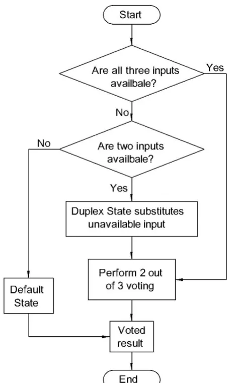
The discrete signals are used to monitor the switch status of BOP components, such as pressure switch signal. Input voting is accomplished by software in the processors, unlike output voting. Besides the input values, the configured Duplex State and Default State may also be used to determine the final voted results. The Duplex State is the substitute value that is used when there are only two available input signals, while the Default State is the value that will be provided directly to the application programs instead of a voted input result. The flow chart of discrete input voting process is shown in Fig. 7.
For three available inputs, the software performs 2 out of 3 voting, with the Duplex State and Default State not used.
If one of the three input values is not available, the software uses the configured Duplex State for performing 2 out of 3 voting, in place of a third actual input. The Duplex State can be set to 0 or 1 according to the actual requirement.
If only one input signal is available or all inputs fail, voting is not performed. The Default State is used instead of the remaining actual input as the final result for the application programs in the processors, which can be set to 0 or 1.
Figure 7. Flow chart of the discrete input voting process
Examples of discrete input voting in all situations are shown in Table1, where the Duplex State is set to 0, the Default State is set 0 and “DI” stands for discrete input.
TABLE 1.
DISCRETE INPUT VOTING EXAMPLES
DI_A DI_B DI_C Voted results
1 1 1 1
1 1 0 1
1 0 0 0
0 0 0 0
1 1 - 1
1 0 - 0
0 0 - 0
- - 0 0
- - - 0
B. Analog Input Voting
maximum, minimum, or an average of the two actual values. The Default State can be configured as the last input state, or a specific maximum or minimum value. The flow chart of analog input voting process is shown in Fig. 8.
Figure 8. Flow chart of the analog input voting process
For three available inputs, the voter compares three corresponding analog input values, which selects the intermediate value. The Duplex State and Default State are not used.
If one input fails, the software uses the configured Duplex State for voting, in place of a third actual input. The intermediate value will still be selected.
If only one input is available or all inputs fail, voting is not performed. The Default State is used as the only input data.
Voting examples of all situations are shown in Table 2. The Duplex State is set to the average of the two actual values and Default State is set to 8.8. “AI” stands for analog input.
TABLE 2.
ANALOG INPUT VOTING EXAMPLES
AI_A AI_B AI_C Voted results
8 9 10 9
- 9 10 9.5
8 - 10 9
8 9 - 8.5
AI_A AI_B AI_C Voted results
- - 10 8.8
- 9 - 8.8
8 - - 8.8
- - - 8.8
C. Discrete Output Voting and Simulation
Voting of discrete output is performed in hardware voter module, which performs 2 out of 3 voting. Before the final result is voted, the output values will be voted twice. For each FPGA, results generated by processors are voted in its output voter for the first time. Then, all voted outputs from the corresponding FPGAs are voted again in the “board voter”. Finally, the final output is produced by each FPGA. Due to the fact that all three FPGAs have the same architecture, anyone can be used to connect to the controlled devices directly or indirectly.
Functional simulation of the output voting is shown in Fig. 9 “FPGA0_cpu0”, “FPGA0_cpu1” and “FPGA0_cpu2” denote the output signals of the processors in the first FPGA, while “output_voter0” is the voted result of the three CPUs. The other FPGAs are denoted in the same way and “voted_result” is the final output.
Figure 9. Functional simulation of output voting
The voting process is accomplished at posedge clk. For the signals of CPUs, suppose ‘1’ is the correct value while ‘0’ means an error in the simulation. It can be seen, each FPGA can tolerate one error at a time. When two of the processors fail in one FPGA, the output of this FPGA board will be faulty. However, the fault can still be masked by the board voter, which can continue work normally. It can be seen that when there are two FPGAs fail, the fault can’t be masked any more. Failure of one FPGA plus one processor is the maximum tolerance of the redundant controller. The results show that the proposed redundant architecture greatly improves the reliability of the controller. It can be used for the subsea BOP control system.
V. CONCLUSIONS AND FUTURE WORK
paper. The contributions of this work can be summarized as:
(1) The proposed hardware architecture is implemented by using three FPGA development boards and RS-232 serial ports are employed to communicate. (2) Nios II System is developed in each FPGA. A
multiprocessor system is implemented to improve reliability of the control system and software is designed to use mutex in order to protect the shared memory.
(3) In order to obtain reliable results, different voting algorithms for discrete input, analog input and discrete output are proposed.
(4) Functional simulation is accomplished and it demonstrates that the proposed controller is able to tolerate faults with high reliability.
In the future research work, the control logic for subsea BOP function, human machine interface graphical design and redundant databases will be developed.
ACKNOWLEDGMENT
The authors wish to acknowledge the financial support of the National High-Technology Research and Development Program of China (No.2007AA09A101), National Natural Science Foundation of China (No.50874115), Project of Science and Technology Development of Shandong Province, "Taishan Scholar" Construction Project Special Fund Project (TS20110823) and Innovation Foundation of Graduate School of China University of Petroleum (No.CXZC11-13).
REFERENCES
[1] W. F. Harlow, B. C. Brantley, and R. M. Harlow, “BP initial image repair strategies after the Deepwater Horizon spill, “ Publ. Relat. Rev, vol. 37, 2011, pp.80-83.
[2] J. E. Skogdalen, I. B. Utne, and J. E. Vinnem, “Developing safety indicators for preventing offshore oil and gas deepwater drilling blowouts,” Saf. Sci. vol. 49, 2011, pp.1187-1199, doi:10.1016/j.ssci.2011.03.012
[3] J. A. Cheatham, J. M. Emmert, and S. Baumgart, “A survey of fault tolerant methodologies for fpgas,” ACM Trans. Des. Autom. Electron. Syst. vol. 11, 2006, pp. 501-533.
[4] K. S. Morgan, D. L. McMurtrey, B. H. Pratt, and M. J. Wirthlin, “A comparison of TMR with alternative fault-tolerant design techniques for FPGAs,” IEEE Trans. Nucl. Sci. vol. 54, 2007, pp. 2065-2072, doi:10.1109/TNS.2007.910871
[5] M. Straka, J. Kastil, and Z. Kotasek, “Fault Tolerant Structure for SRAM-Based FPGA via Partial Dynamic Reconfiguration Digital System Design,” Proc. - Euromicro Conf. Digit. Syst. Des.: Archit., Methods Tools, DSD, 2010, pp. 365-372, doi: 10.1109/DSD.2010.12 [6] X. X. She and K. S. McElvain, “Time Multiplexed Triple
Modular Redundancy for Single Event Upset Mitigation,” IEEE Trans. Nucl. Sci, vol. 56, 2009, pp. 2443-2448, doi: 10.1109/TNS.2009.2021656
[7] B. Pratt, M. Caffrey, J. F. Carroll, P. Graham, K. Morgan, and et al. “Fine-grain SEU mitigation for FPGAs using partial TMR,” IEEE Trans. Nucl. Sci. vol. 55, 2008, pp. 2274-2280, doi:10.1109/TNS.2008.2000852
[8] L. Sterpone and M. Violante, “A new reliability-oriented place and route algorithm for SRAM-based FPGAs,” IEEE Trans. Comput., vol. 55, no.6, pp. 732-744, Jun. 2006. [9] S. Golshan and E. Bozorgzadeh, “SEU-aware resource
binding formodular redundancy based designs on FPGA,” in Proc. DATE, Apr.2009, pp. 1124-1129.
[10]R. Marzotto, P.Zoratti, D. Bagni, A. Colombari, and V.Murino, “A real-time versatile roadway path extraction and tracking on an FPGA platform,” Comput Vision Image Understanding, vol. 114, 2010, pp. 1164-1179, doi:10.1016/j.cviu.2010.03.015
[11]A. Astarloa, J. Lázaro, U. Bidarte, J. Jiménez, and A.Zuloaga, “FPGA technology for multi-axis control systems,” Mechatronics, vol. 19, 2009, pp. 258-268, doi:10.1016/j.mechatronics.2008.09.001
[12]A. Kothare, I. Mirza, K. P. Singh, and A. F. Abbey, “FPGA-based flexible CCD control system for X-ray astronomy payloads,” Nucl Instrum Methods Phys Res Sect A, vol. 604, 2009, pp. 747-754, doi:10.1016/j.nima.2009.01.103
[13]D. Chaikalis, N. Sgouros, D. Maroulis, and P. Papageorgas, “Hardware implementation of a disparity estimation scheme for real-time compression in 3D imaging applications,” J Visual Commun Image Represent, vol. 19, 2008, pp. 1-11, doi:10.1016/j.jvcir.2007.09.003
[14]R.V. Kshirsagar and R.M. Patrikar, “Design of a novel fault-tolerant voter circuit for TMR implementation to improve reliability in digital circuits,” Microelectron. Reliab. vol. 49, 2009, pp. 1573-1577, doi:10.1016/j.microrel.2009.08.001
[15]T. Dorta, J. Jimenez, J. L. Martin, U. Bidarte, and A. Astarloa, “overview of FPGA-Based Multiprocessor systems,” ReConFig - Int. Conf. ReConFigurable Comput. FPGAs, 2009, pp. 273-278, doi: 10.1109/ReConFig.2009.15
[16]R. Sadoun, A. Belouchrani, E. B. Bourennane, and A. Zerguerras, “An FPGA based soft multiprocessor for DNS/DNSSEC authoritative server,” Microprocessors Microsyst, vol. 35, 2011, pp. 473-483, doi:10.1016/j.micpro.2011.03.004
[17]M. Beltrán, A. Guzmán, and F. Sevillano, “High level performance metrics for FPGA-based multiprocessor systems,” Perform Eval, vol. 67, 2010, pp. 417-431, doi:10.1016/j.peva.2009.12.004
[18]D. Zydek and H. Selvaraj, “Hardware implementation of processor allocation schemes for mesh-based chip multiprocessors,” Microprocessors Microsyst, vol. 34, 2010, 39-48, doi:10.1016/j.micpro.2009.11.003
[19]B. P. Cai, Y. H. Liu, Z. K. Liu, F. Wang, X. J. Tian, and et al, “Development of Automatic Subsea Blowout Preventer Stack Control System using PLC based SCADA,” unpublished.
[20]Nios UART, ALTERA, <http://www.altera.com/literature /ds/ds_nios_uart.pdf>
[21]Introduction, Nios II Processor Reference Handbook, ALTERA, <http://www.altera.com.cn/literature/hb/nios2/ n2cpu_nii51001.pdf>
[22]Creating multiprocessor Nios II system tutorial, ALTERA 2011,<www.altera.com/literature/tt/tt_nios2_multiprocesso r_ tutorial.pdf>
[24]Avalon Interface Specifications, ALTERA, < www.altera.com/literature/manual/mnl_avalon_spec.pdf>
Zengkai Liu wasborn in Shandong, P. R. China, in 1986. He received his B.S. and M.S. degree in Mechanical Engineering from China University of Petroleum in 2009 and 2011 respectively. Currently, he is a Ph.D. candidate in Mechanical Engineering in China University of Petroleum, P. R. China. His recent research interest is the Field Programmable Gate Array based control system for subsea blowout preventer.
Yonghong Liu was born in Anhui, P. R. China, in 1965. He received his Ph.D. degree in Mechanical Manufacture from Harbin Institute of Technology, Harbin, China, in 1996.
He is currently a professor and doctoral supervisor in College of Electromechanical Engineering at China University of Petroleum, China. He has published over 120 papers in some international or national journals and conferences. His current research interests include the Expansion Sand Screen for sand control, new kind of numerical control machine about combined machining and control system of the subsea drilling equipments. Dr. Liu is a member of China Nontraditional Machining Committee and Nontraditional Machining Association of Shandong. Dr. Liu is the candidate for the New Century National “Hundred, Thousand and Ten Thousand Talents Project” and prominent young and middle-aged specialist of Shandong Province.
Baoping Cai was born in Hebei, P. R. China, in 1982. He received his B.S. and M.S. degree in Mechanical Engineering from China University of Petroleum in 2006 and 2008 respectively. Currently, he is a Ph.D. candidate in Mechatronic Engineering in China University of Petroleum, P. R. China. His
recent research interest is the control system of the subsea drilling equipments.
Fei Wang was born in Shandong, P. R. China, in 1985. He received his B.S. and M.S. degree in Mechanical Engineering from China University of Petroleum in 2008 and 2010 respectively. Currently, he is a Ph.D. candidate in Mechanical Design and Theory in China University of Petroleum, China. His recent research interest is the control system of NC machine tool.
Zhili Chen was born in Shanxi, P. R. China, in 1984. He received his B.S. degree in Machinery Design and Manufacturing and Its Automation from China University of Petroleum in 2009. Currently, he is a postgraduate student in Mechanical Engineering in China University of Petroleum, P. R. China. His recent research interest is the design of NC machining simulation system
Xiaojie Tian wasborn in Shandong, P. R. China, in 1985. He received his B.S. and M.S. degree in Mechanical Engineering from China University of Petroleum in 2008 and 2010 respectively. Currently, he is a Ph.D. candidate in Mechanical Design and Theory in China University of Petroleum, China. His recent research interest is the control system of the subsea drilling equipments based on the field bus.