1139 | P a g e
LOW POWER HIGH PERFORMANCE PULSED FLIP
FLOPS BASED ON SIGNAL FEED SCHEME
Juhi Rastogi
1, Vipul Bhatnagar
21,2
Department of Electronics and Communication,
Inderprastha Enginering College, Ghaziabad (India)
ABSTRACT
Flip-flops are critical timing elements in digital circuits which have a large impact on circuit speed and power consumption. The performance of the Flip-Flop is an important element to determine the performance of the whole synchronous circuit. In this paper, a dual-edge triggered flip-flop with high performance is designed.This paper discussed a low-power flip-flop (FF) design features an explicit type pulse-triggered configuration and a customized true single phase clock latch based on a signal feed-through scheme is\ presented. The proposed design effectively over come on the problem of the long discharging path in conventional explicit type pulse-triggered FF (P-FF) designs and attain better speed and power performance.
Keywords: P-Ff (Pulsed Flip Flop), Low Power, Ff (Flip Flop)
I. INTRODUCTION
In the past few ten years, according Moore‟s law the VLSI technology continuously increase the transistor
densities, there are hundreds millions billions of transistors are fabricated on a chip today, which constantly
increase the power consumption of the chip. Flip-Flops are very important circuit elements in all synchronous
VLSI circuits. Flip flops consumes a significant portion of the total power of the circuit so they are not only
responsible for the correct timing, performance and functionality of the chip, but also on the other clock
distribution networks.
Pulse-triggered flip flops are characterized by an uncomplicated structure, negative setup time and soft edge,
improved performance over traditional master slave flip flop. There are various types of pulse-triggered flip
flops were recently proposed. It includes implicit-pulsed flip flops and explicit-pulsed flip flops. The pulse
generator of the explicit-pulsed flip flop can be shared by neighboring identical flip flops, which contribute to
less power dissipation than implicit-pulsed ones. The clock frequency can reduce to half in dual-edge flip flops
that of the single-edge triggered flip flops while maintaining the same data throughput, consequently power
dissipation is decreased.
In this paper, we present a novel low-power and high performance pulsed flip flop design based on a signal feed
through method. Observing the delay inconsistency in latching data „‟1‟‟ and ‟‟0”. This flip flop design
manages, how to shorten the longer delay, this will done by feeding the input signal directly to an internal node
of the latch design. This will helps to speed up the data transition. This method isimplemented by introducing a
uncomplicated and a very simple pass transistor which used to drive the extra signal. After combining this
circuit method with the pulse generation circuitry, it forms a new pulsed flip flop design with improved speed
1140 | P a g e
II. PROPOSED DESIGN BASED ON SIGNAL FEED THROUGH METHOD
2.1
Conventional Explicit Pulsed Flip Flop
Pulse-triggered flip-flops can be static, or semi-static, or dynamic, or semi-dynamic. Pulse-triggered flip-flops
can also be classified into single-edge triggered flip-flops and double-edge triggered flip flops. the pulse
triggered flip-flops based on the pulse generators can be categorized into two types: implicit pulsed flip flops
and explicit-pulsed flip flop. The pulse is generated inside the flip-flop in implicit-pulse triggered flip flops, or
ip-FF. While in explicit-pulse triggered flip-flops, the pulse is generated externally.
To provide a fine comparison there are few existing designs are discussed. A classic explicit P-FF design,
named data-close-to- output (ep-DCO) .Pulsed flip-flops offer an attractive method of meeting delay and energy
requirements of a design while providing the-borrowing capability to mitigate clock skew effects. For
high-speed operation, ip-DCO has the fastest delay of any flip-flop considered, along with a large amount of negative
setup time.This design ep-DCO suffers from a serious drawback and that is the internal node X is discharged on
every rising edge of the clock despite of the presence of a static input “1”. This gives rise to large switching
power dissipation.
To overcome the above discussed problem of ep-DCO flip flop there are many remises are introduced such as
conditional discharge, conditional precharge, conditional capture etc. A modified version is shown in fig (b) an
extra nMOS transistor MN3 controlled by the output signal Q_fdbk is working in CDFF flip flop thus there is
no discharge occurs if the input data remains at 1.
Fig.(a) ep-DCO Fig.(b) CDFF
1141 | P a g e
SCDFF which is shown in fig (c),differs from the CDFF design in using a static latch structure. Node X is thus
exempted from periodical precharges. It exhibits a longer data-to-Q (D-to-Q) delay than the CDFF design. Both
designs face a worst case delay caused by a discharging path consisting of three stacked transistors, i.e., MN1–
MN3. To overcome this drawback modified hybrid latch flip flop is introduced which is shown in fig (d).A
powerful pull-down circuitry is needed to increase the speed which causes extra layout area and power
consumption. In this flip flop the keeper logic at node X is removed. Although this circuit is simple, but it
encounters two drawbacks. First, since node X is not predischarged, a delayed 0 to 1 delay is expected. Second,
node X becomes floating in certain cases and its value may float causing extra dc power.
2.2 Proposed Pulsed Flip Flop
Recall the four circuits which are reviewed previously, they all are suffers from the same worst case timing
problem which is occurring at 0 to 1 data transitions. Referring to the Fig. 2, the proposed design uses a signal
feed-through technique to improve this delay. Comparable to the SCDFF design, the proposed design also
employs a static latch structure and a conditional discharge scheme to avoid redundant switching at an internal
node. On the other hand, there are three main differences that lead to a only one of its kind TSPC latch structure
and create the proposed design different from the previous one which are explained above.
In this FF at First, there is a weak pull-up pMOS transistor MP1, the gate of this transistor is connected to the
ground which is used in the first stage of the TSPC latch. This method of transistor will give the rise to a
pseudo-nMOS logic technique of design, and the charge keeper circuit for the internal node X can be saved. In
result to the circuit simplicity, this approach also reduces the load capacitance of node X.
Now the second point is, a pass transistor MNx is included which is controlled by the pulse clock thus the input
data can drive node Q of the latch directly through the signal feed-through scheme. Beside with the pull-up
transistor MP2 at the second stage inverter of the TSPC latch, this additional passage facilitates supplement the
signal driving from the input source to node Q. The node level therefore be a quickly pulled up to shorten the
data transition delay.
Now the pull-down network of the second stage inverter is completely removed. As a substitute the newly
employed pass transistor MNx provides a discharging path.
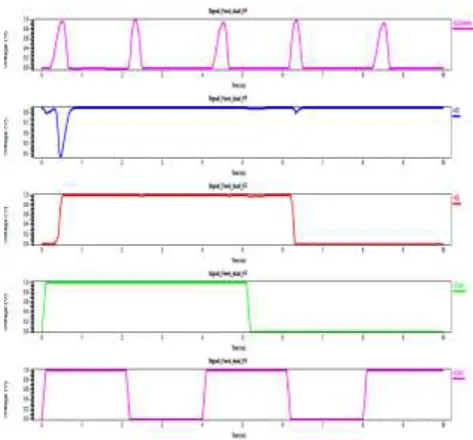
III. SCHEMATIC AND SIMULATION RESULT
1142 | P a g e
SOURCES SIMULATION RESULT
The working principles of the proposed design are explained as follows:
When a clock pulse arrives, when there is no data transition occurs, the input data and node Q have
identical level, when current passes through the pass transistor MNx, which keeps the input stage of the
flip flop from. At similar time, the input data and the output feedback Q_fdbk assume opposite signal
levels and the pull-down path of node X is turned off. Hence, no signal switching occurs at any internal
nodes.
When “0” to “1”(low to high) data transition occurs, node X will discharge and transistor MP2 will turn
on which at that time pulls node Q high this corresponds to the worst case of timing of the flip flop
operations as the discharging path conducts no more than for a pulse duration. Though, with the signal
feed through scheme, the delay can be greatly shortened by a boost that can be obtained from the input
source via the pass transistor MNx . Even though this seems a load to the input source with straight
charging/discharging dependability which is a common drawback of all pass transistor logic, the
1143 | P a g e
When “1” to “0”(high to low) data transition occurs, pass transistor MNx is similarly turned by the
clock pulse and node Q is discharged by the input stage all the way through this path. Contrasting the
case of “0” to “1” data transition, the input source bears the one and only discharging dependability.
Because MNx is turned on only for a short time period, the loading consequence to the input source is
not considerable. In exacting this discharging does not communicate to the critical path delay and calls
for no transistor size change to improve the speed. In calculation because a keeper logic is placed at
node Q, the discharging responsibility of the input source is lift once the situation of the keeper logic is
inverted.
Transistor MP1 is permanently ON because gate of the transistor is ground.
3.2 Schematic of Dual Edge P-Ff
PULSED GENERATOR
1144 | P a g e
SIMULATION RESULT
IV. RESULT ANALYSIS
Table I shows the comparative analysis of dual edge flip flops using 90 nm technology and supply voltage 1v.
The concert of the proposed pulsed flip flop design is evaluated beside existing designs through simulations.
The compared designs consist of four explicit type pulsed flip flops designs which are shown above. There is an
implicit type pulsed flip flop design named SDFF is also mentioned. All pulsed flip flop designs used a
conventional CMOS NAND-logic-based pulse generator design with a three-stage inverter chain excluding the
MHLFF design, which employs its own pulse generation circuitry.Because pulse width design is critical to the
accuracy of data capture in addition to the power consumption, the transistors of the pulse generator logic are
sized for a design of 120 ps in pulse width in the case. In addition the sizing ensures that the pulse generators
can perform correctly in each and every process corners. Through consider to the latch structures, every pulsed
flip flop design is independently optimized issue to the product of D-to-Q delay and power. To imitate the signal
rise and fall time delays, input signals are generated all the way through buffers. While the proposed design
requires direct output driving as of the input source, in favor of reasonable comparisons the power consumption
of the data input buffer (an inverter) is incorporated.
Table II and table III defines the summarized features of the circuit and the simulation results. In favor of circuit
properties, while the proposed design does not utilize the least number of transistors. This is essentially credited
to the signal feed-through method which mostly reduces the transistor sizes on thedischarging path. In terms of
power behavior, the proposed design is the mainly proficient in five out of the six test patterns. The savings
differs in different combination of test pattern and flip flop design. It is power saving against ep-DCO, CDFF,
SCDFF andMHLFF. The ep-DCO design consumes the major portion of power as of the extra internal node
1145 | P a g e
SINGLE EDGE FLIP FLOP TABLE I DUAL EDGE FLIP FLOP TABLE II
LEAKAGE CURRENT (nW) IN DUAL EDGE P-FF TABLE III
V. CONCLUSION
In this paper, there are five flip flops are discussed and compared. Both single edge and dual edge flip flops are
discussed. The main idea of this signal feed design is to increase power and speed performance. Dual edge
triggered flip flop are basically consumed less power. In this thesis, there is a novel pulsed flip flop design by
employing a customized TSPC latch structure which incorporate a mixed design style that consist a pass
transistor and a pseudo-nMOS logic. The main idea was to supply a signal feed through from input source to the
internal node of the latch, which would make possible additional driving to cut down the transition time and
improve both power and speed performance. The design was cleverly achieved by employing a uncomplicated
pass transistor. General simulations were conducted, and the results did carry the claims of the proposed design
in a wide range of performance aspect.By the comparison table I, II, III it is clear that proposed design has least
delay, power switching activity, number of transistor and leakage current in comparison with all discussed flip
flops.
REFERENCES
[1] Jin-Fa Lin,”Low-Power Pulse-Triggered Flip-Flop Design Based on a Signal Feed-Through Scheme”,
IEEE TRANSACTIONS ON VERY LARGE SCALE INTEGRATION (VLSI) SYSTEMS, VOL. 22, NO. 1, JANUARY 2014
FF Power(uW)
50%
Switching
Delay(ps) Number of
transistors
epDCO 23.42541 198.81 28
CDFF 22.3876 200.74 30
MHLLF 19.66693 101.67 19
SCDFF 24.35541 191.86 31
Signal
feed
25.27361 393.46 24
Flip Flops Power (uW) 100% switching PDP at 50% switching (pJ) Delay (ps) Power (uW) 50% Switching
epDCO 30.5368 5.39 198.25 27.2278
CDFF 28.6858 5.64 263.53 21.42264
SCDFF 29.6388 5.46 250.97 21.77347
MHLLF 31.8159 8.82 445.56 19.81702
Signal
feed
24.838 4.17 212.09 19.67952
epDCO CDFF MHLFF Static
CDFF
Signal
feed
(CLK,Data)
(0,0)
74.11 42.04 48.78 38.68 47.24
(CLK,Data)
(1,1)
1146 | P a g e
[2] J. Tschanz, S. Narendra, Z. Chen, S. Borkar, M. Sachdev, and V. De, “Comparative delay and energy of
single edge-triggered and dual edge triggered pulsed flip-flops for high-performance microprocessors,” in
Proc. ISPLED, 2001, pp. 207–212.
[3] P. Zhao, T. Darwish, and M. Bayoumi, “High-performance and low power conditional discharge flip-flop,”
IEEE Trans. Very Large ScaleIntegr. (VLSI) Syst., vol. 12, no. 5, pp. 477–484, May 2004.
[4] M.-W. Phyu, W.-L. Goh, and K.-S. Yeo, “A low-power static dual edgetriggered flip-flop using an
output-controlled discharge configuration,” in Proc. IEEE Int. Symp. Circuits Syst., May 2005, pp. 2429–2432.
[5] S. H. Rasouli, A. Khademzadeh, A. Afzali-Kusha, and M. Nourani, “Low power single- and
double-edge-triggered flip-flops for high speed applications,” IEE Proc. Circuits Devices Syst., vol. 152, no. 2, pp. 118–
122, Apr. 2005.
[6] Nikola Nedovic, William W Walker,”ALow Power Symmetrically Pulsed Dual Edge-Triggered
Flip-Flop,”in Fujitsu Laboratories of AmericaInc., 595 Lawrence Expressway,Sunnyvale, CA 94086-3922,
2002.
[7] J. Tschanz, S. Narendra, Z. Chen, S. Borkar, M. Sachdev, and V. De, “Comparative delay and energy of
single edge-triggered and dual edge triggered pulsed flip-flops for high performance microprocessors,” in
Proc. ISPLED, 2001, pp. 207–212.
[8] K. Chen, “A 77% energy saving 22-transistor single phase clocking D-flip-flop with adoptive-coupling
configuration in 40 nm CMOS,” in Proc. IEEE Int. Solid-State Circuits Conf., Nov. 2011, pp. 338–339.
[9] E. Consoli, M. Alioto, G. Palumbo, and J. Rabaey, “Conditional pushpull pulsed latch with 726 fJops
energy delay product in 65 nm CMOS,” in Proc. IEEE Int. Solid-State Circuits Conf., Feb. 2012, pp. 482–
483.
[10] N. Nedovic, M. Aleksic, and V. G. Oklobdzija, “Conditional precharge techniques for power-efficient
dual-edge clocking,” in Proc. Int. Symp.Low-Power Electron. Design, Aug. 2002, pp. 56–59.
[11] Xue-Xiang Wu and Ji-Zhong Shen,” Low-power explicit-pulsed triggered flip–flop with robust output,”
Electronics letter, Vol. 48 No. 24, November 2012.
[12] Y.-T. Hwang, J.-F. Lin, and M.-H. Sheu, “Low power pulsetriggered flip-flop design with conditional
pulse enhancement scheme,” IEEE Trans. Very Large Scale Integr. (VLSI) Syst., vol. 20, no. 2, pp. 361–
366, Feb. 2012.
[13] H. Mahmoodi, V. Tirumalashetty, M. Cooke, and K. Roy, “Ultra low power clocking scheme using energy
recovery and clock gating,” IEEETrans. Very Large Scale Integr. (VLSI) Syst., vol. 17, no. 1, pp. 33–44,
Jan. 2009.
[14] P. Zhao, J. McNeely, S. Venigalla, G. P. Kumar, M. Bayoumi, N. Wang, and L. Downey,
“Clocked-pseudo-NMOS flip-flops for level conversion in dual supply systems,” IEEE Trans. Very Large Scale
Integr. (VLS ZI)Syst., vol. 17, no. 9, pp. 1196–1202, Sep. 2009.
[15] V. G. Oklobdzija, “Clocking and clocked storage elements in a multi gigahertz environment,” IBM J. Res.
Devel., vol. 47, no. 5, pp. 567–584, Sep. 2003.
[16] Goh Wang Ling, Yeo Kiat Seng, *Zhang Wenle and Lim Hoe Gee,” A Novel Static Dual Edge-Trigger
Flip-flop for High-Frequency Low-Power Application,” IEEE International Symposium on Integrated
1147 | P a g e
[17] Peiyi Zhao,” Low-Power Clocked-Pseudo-NMOS Flip-Flop for Level Conversion in Dual Supply
Systems,” IEEE TRANSACTIONS ON VERY LARGE SCALE INTEGRATION (VLSI) SYSTEMS,
VOL. 17, NO. 9, SEPTEMBER 2009.
[18] S. Sadrossadat, H. Mostafa, and M. Anis, “Statistical design framework of sub-micron flip-flop circuits
considering die-to-die and within-die variations,” IEEE Trans. Semicond. Manuf., vol. 24, no. 2, pp. 69–79,
Feb. 2011.
[19] Myint Wai Phyu,” Power-Efficient Explicit-Pulsed Dual-Edge Triggered Sense-Amplifier Flip-Flops,”
IEEE TRANSACTIONS ON VERY LARGE SCALE INTEGRATION (VLSI) SYSTEMS, VOL. 19, NO.
1, JANUARY 2011.
[20] Yin-Tsung Hwang, Jin-Fa Lin, and Ming-Hwa Sheu,” Low-Power Pulse-Triggered Flip-Flop Design with
Conditional Pulse-Enhancement Scheme,” IEEE TRANSACTIONS ON VERY LARGE SCALE